SMS05C, SMS12C, SMS15C, SMS24C 5−Line Transient Voltage Suppressor Array
This 5−line voltage transient suppressor array is designed for application requiring transient voltage protection capability. It is intended for use in over−transient voltage and ESD sensitive equipment such as computers, printers, automotive electronics, networking communication and other applications. This device features a monolithic common anode design which protects five independent lines in a single SC−74 package.
Features http://onsemi.com
SC−74 FIVE TRANSIENT VOLTAGE SUPPRESSOR 350 W PEAK POWER
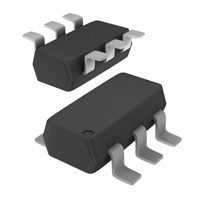
PIN ASSIGNMENT
1 6 1 SC−74 CASE 318F STYLE 6 2 3 PIN 1. 2. 3. 4. 5. 6. 6 5 4 CATHODE ANODE CATHODE CATHODE CATHODE CATHODE
• Protects up to 5 Lines in a Single SC−74 Package • Peak Power Dissipation − 350 W (8 20 ms Waveform) • ESD Rating of Class 3B (Exceeding 8.0 kV) per Human Body Model • • • • • • • •
and Class C (Exceeding 400 V) per Machine Model Compliance with IEC 61000−4−2 (ESD) 15 kV (Air), 8.0 kV (Contact) Flammability Rating of UL 94 V−0 Pb−Free Package is Available
Applications
Hand−Held Portable Applications Networking and Telecom Automotive Electronics Serial and Parallel Ports Notebooks, Desktops, Servers
MARKING DIAGRAM
6xM
MAXIMUM RATINGS (TJ = 25°C unless otherwise specified)
Symbol PPK 1 Rating Peak Power Dissipation 8 20 ms Double Exponential Waveform (Note 1) Operating Junction Temperature Range Storage Temperature Range Lead Solder Temperature (10 s) Human Body Model ( HBM) Machine Model (MM) IEC 61000−4−2 Air (ESD) IEC 61000−4−2 Contact (ESD) Value 350 Unit W
x = SMS05C:J = SMS12C:K = SMS15C:L = SMS24C:M M = Date Code
TJ TSTG TL ESD
−40 to 125 −55 to 150 260 >8000 >400 >15000 >8000
°C °C °C V
ORDERING INFORMATION
Device SMS05CT1 SMS12CT1 SMS15CT1 SMS15CT1G SMS24CT1 Package SC−74 SC−74 SC−74 SC−74 (Pb−Free) SC−74 Shipping† 3000/Tape & Reel 3000/Tape & Reel 3000/Tape & Reel 3000/Tape & Reel 3000/Tape & Reel
Maximum ratings are those values beyond which device damage can occur. Maximum ratings applied to the device are individual stress limit values (not normal operating conditions) and are not valid simultaneously. If these limits are exceeded, device functional operation is not implied, damage may occur and reliability may be affected. 1. Non−repetitive current pulse per Figure 3.
†For information on tape and reel specifications, including part orientation and tape sizes, please refer to our Tape and Reel Packaging Specification Brochure, BRD8011/D.
© Semiconductor Components Industries, LLC, 2005
1
February, 2005 − Rev. 5
Publication Order Number: SMS05C/D
�SMS05C, SMS12C, SMS15C, SMS24C
SMS05C ELECTRICAL CHARACTERISTICS (TJ = 25°C unless otherwise specified)
Parameter Reverse Working Voltage Breakdown Voltage Reverse Leakage Current Clamping Voltage Clamping Voltage Maximum Peak Pulse Current Capacitance Symbol VRWM VBR IR VC VC IPP CJ (Note 2) IT = 1.0 mA (Note 3) VRWM = 5.0 V IPP = 5.0 A (8 IPP = 24 A (8 8 20 ms Waveform) 20 ms Waveform) 6.2 Conditions Min Typ Max 5.0 7.2 5.0 9.8 14.5 24 260 400 Unit V V mA V V A pF
20 ms Waveform
VR = 0 V, f = 1.0 MHz (Line to GND)
SMS12C ELECTRICAL CHARACTERISTICS (TJ = 25°C unless otherwise specified)
Parameter Reverse Working Voltage Breakdown Voltage Reverse Leakage Current Clamping Voltage Clamping Voltage Maximum Peak Pulse Current Capacitance Symbol VRWM VBR IR VC VC IPP CJ (Note 2) IT = 1.0 mA (Note 3) VRWM = 12 V IPP = 5.0 A (8 IPP = 15 A (8 8 20 ms Waveform) 20 ms Waveform) 13.3 0.001 Conditions Min Typ Max 12 15 1.0 19 23 15 120 150 Unit V V mA V V A pF
20 ms Waveform
VR = 0 V, f = 1.0 MHz (Line to GND)
SMS15C ELECTRICAL CHARACTERISTICS (TJ = 25°C, unless otherwise specified) (See Note 4)
Parameter Reverse Working Voltage Breakdown Voltage Reverse Leakage Current Clamping Voltage Clamping Voltage Maximum Peak Pulse Current Capacitance Symbol VRWM VBR IR VC VC IPP CJ (Note 2) IT = 1.0 mA (Note 3) VRWM = 15 V IPP = 5.0 A (8 IPP = 12 A (8 8 20 ms Waveform) 20 ms Waveform) 17 0.05 Conditions Min Typ Max 15 19 1.0 24 29 12 95 125 Unit V V mA V V A pF
20 ms Waveform
VR = 0 V, f = 1.0 MHz (Line to GND)
SMS24C ELECTRICAL CHARACTERISTICS (TJ = 25°C, unless otherwise specified)
Parameter Reverse Working Voltage Breakdown Voltage Reverse Leakage Current Clamping Voltage Clamping Voltage Maximum Peak Pulse Current Capacitance Symbol VRWM VBR IR VC VC IPP CJ (Note 2) IT = 1.0 mA (Note 3) VRWM = 24 V IPP = 5.0 A (8 IPP = 8 A (8 8 20 ms Waveform) 20 ms Waveform) 26.7 0.001 Conditions Min Typ Max 24 32 1.0 40 44 8.0 60 75 Unit V V mA V V A pF
20 ms Waveform
VR = 0 V, f = 1.0 MHz (Line to GND)
2. TVS devices are normally selected according to the working peak reverse voltage (VRWM), which should be equal or greater than the DC or continuous peak operating voltage level. 3. VBR is measured at pulse test current IT. 4. Parametrics are the same for the Pb−Free packages, which are suffixed with a “G’’.
http://onsemi.com
2
�SMS05C, SMS12C, SMS15C, SMS24C
TYPICAL PERFORMANCE CURVES (TJ = 25°C unless otherwise specified)
PEAK PULSE DERATING IN % OF PEAK POWER OR CURRENT @ TA = 25 ° C 100 % OF PEAK PULSE CURRENT 90 80 70 60 50 40 30 20 10 0 0 25 50 75 100 125 150 175 200 100 90 80 70 60 50 40 30 20 10 0 0 20 40 t, TIME (ms) 60 80 tP tr PEAK VALUE IRSM @ 8 ms PULSE WIDTH (tP) IS DEFINED AS THAT POINT WHERE THE PEAK CURRENT DECAY = 8 ms HALF VALUE IRSM/2 @ 20 ms
TA, AMBIENT TEMPERATURE (°C)
Figure 1. Pulse Derating Curve
Figure 2. 8 × 20 ms Pulse Waveform
300 JUNCTION CAPACITANCE (pF)
50 VC, CLAMPING VOLTAGE (V) 45 40 35 30 25 20 15 10 5 0 0 5
SMS24C
8 x 20 ms PULSE WAVEFORM
f = 1.0 MHz
250 200 SMS05C 150 100 SMS12C 50 0 0 5 10 SMS15C 15 SMS24C 20 25
SMS15C SMS12C
SMS05C
10
15
20
25
IPP, PEAK PULSE CURRENT (A)
VBR, REVERSE VOLTAGE (V)
Figure 3. Clamping Voltage vs. Peak Pulse Current
Figure 4. Junction Capacitance vs. Reverse Voltage
Figure 5. ESD Pulse IEC 61000−4−2 (8.0 kV Contact)
Figure 6. SMS15CT1 ESD Response for IEC 61000−4−2 (+8.0 kV Contact)
http://onsemi.com
3
�SMS05C, SMS12C, SMS15C, SMS24C
TYPICAL COMMON ANODE APPLICATIONS A 5 TVS junction common anode design in a SC-74 package protects four separate lines using only one package. This adds flexibility and creativity to PCB design especially when board space is at a premium. A simplified example of SMS05C Series Device applications is illustrated below.
A KEYBOARD TERMINAL PRINTER ETC. B I/O C D E FUNCTIONAL DECODER
GND SMS05C SERIES DEVICE
Figure 7. Computer Interface Protection
VDD VGG ADDRESS BUS RAM ROM
DATA BUS I/O
CPU CLOCK
CONTROL BUS
GND SMS05C SERIES DEVICE
Figure 8. Microprocessor Protection
http://onsemi.com
4
�SMS05C, SMS12C, SMS15C, SMS24C
PACKAGE DIMENSIONS
SC−74 CASE 318F−05 ISSUE K
NOTES: 1. DIMENSIONING AND TOLERANCING PER ANSI Y14.5M, 1982. 2. CONTROLLING DIMENSION: INCH. 3. MAXIMUM LEAD THICKNESS INCLUDES LEAD FINISH THICKNESS. MINIMUM LEAD THICKNESS IS THE MINIMUM THICKNESS OF BASE MATERIAL.
A L
6 5 1 2 4
S
3
B
DIM A B C D G H J K L M S
D G M 0.05 (0.002) H C K J
INCHES MIN MAX 0.1142 0.1220 0.0512 0.0669 0.0354 0.0433 0.0098 0.0197 0.0335 0.0413 0.0005 0.0040 0.0040 0.0102 0.0079 0.0236 0.0493 0.0649 0_ 10 _ 0.0985 0.1181
MILLIMETERS MIN MAX 2.90 3.10 1.30 1.70 0.90 1.10 0.25 0.50 0.85 1.05 0.013 0.100 0.10 0.26 0.20 0.60 1.25 1.65 0_ 10 _ 2.50 3.00
STYLE 6: PIN 1. CATHODE 2. ANODE 3. CATHODE 4. CATHODE 5. CATHODE 6. CATHODE
SOLDERING FOOTPRINT*
2.4 0.094
1.9 0.074 0.7 0.028
0.95 0.037 0.95 0.037
1.0 0.039
SCALE 10:1
mm inches
*For additional information on our Pb−Free strategy and soldering details, please download the ON Semiconductor Soldering and Mounting Techniques Reference Manual, SOLDERRM/D.
http://onsemi.com
5
�SMS05C, SMS12C, SMS15C, SMS24C
ON Semiconductor and are registered trademarks of Semiconductor Components Industries, LLC (SCILLC). SCILLC reserves the right to make changes without further notice to any products herein. SCILLC makes no warranty, representation or guarantee regarding the suitability of its products for any particular purpose, nor does SCILLC assume any liability arising out of the application or use of any product or circuit, and specifically disclaims any and all liability, including without limitation special, consequential or incidental damages. “Typical” parameters which may be provided in SCILLC data sheets and/or specifications can and do vary in different applications and actual performance may vary over time. All operating parameters, including “Typicals” must be validated for each customer application by customer’s technical experts. SCILLC does not convey any license under its patent rights nor the rights of others. SCILLC products are not designed, intended, or authorized for use as components in systems intended for surgical implant into the body, or other applications intended to support or sustain life, or for any other application in which the failure of the SCILLC product could create a situation where personal injury or death may occur. Should Buyer purchase or use SCILLC products for any such unintended or unauthorized application, Buyer shall indemnify and hold SCILLC and its officers, employees, subsidiaries, affiliates, and distributors harmless against all claims, costs, damages, and expenses, and reasonable attorney fees arising out of, directly or indirectly, any claim of personal injury or death associated with such unintended or unauthorized use, even if such claim alleges that SCILLC was negligent regarding the design or manufacture of the part. SCILLC is an Equal Opportunity/Affirmative Action Employer. This literature is subject to all applicable copyright laws and is not for resale in any manner.
PUBLICATION ORDERING INFORMATION
LITERATURE FULFILLMENT: Literature Distribution Center for ON Semiconductor P.O. Box 61312, Phoenix, Arizona 85082−1312 USA Phone: 480−829−7710 or 800−344−3860 Toll Free USA/Canada Fax: 480−829−7709 or 800−344−3867 Toll Free USA/Canada Email: orderlit@onsemi.com N. American Technical Support: 800−282−9855 Toll Free USA/Canada Japan: ON Semiconductor, Japan Customer Focus Center 2−9−1 Kamimeguro, Meguro−ku, Tokyo, Japan 153−0051 Phone: 81−3−5773−3850 ON Semiconductor Website: http://onsemi.com Order Literature: http://www.onsemi.com/litorder For additional information, please contact your local Sales Representative.
http://onsemi.com
6
SMS05C/D
�