SN54/74LS670
4 x 4 REGISTER FILE
WITH 3-STATE OUTPUTS
The TTL / MSI SN54 / 74LS670 is a high-speed, low-power 4 x 4 Register
File organized as four words by four bits. Separate read and write inputs, both
address and enable, allow simultaneous read and write operation.
The 3-state outputs make it possible to connect up to 128 outputs to increase the word capacity up to 512 words. Any number of these devices can
be operated in parallel to generate an n-bit length.
The SN54 / 74LS170 provides a similar function to this device but it features
open-collector outputs.
•
•
•
•
•
Simultaneous Read / Write Operation
Expandable to 512 Words by n-Bits
Typical Access Time to 20 ns
3-State Outputs for Expansion
Typical Power Dissipation of 125 mW
4 x 4 REGISTER FILE
WITH 3-STATE OUTPUTS
LOW POWER SCHOTTKY
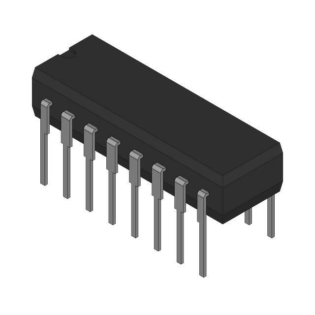
J SUFFIX
CERAMIC
CASE 620-09
16
1
CONNECTION DIAGRAM DIP (TOP VIEW)
VCC
16
D1
15
WA
14
WB
13
EW
12
ER
11
Q1
Q2
10
9
N SUFFIX
PLASTIC
CASE 648-08
16
1
NOTE:
The Flatpak version
has the same pinouts
(Connection Diagram) as
the Dual In-Line Package.
D SUFFIX
SOIC
CASE 751B-03
16
1
1
D2
2
D3
3
D4
4
RB
5
RA
6
Q4
7
Q3
8
GND
ORDERING INFORMATION
PIN NAMES
HIGH
D1 – D4
WA, WB
EW
RA, RB
ER
Q 1 – Q4
SN54LSXXXJ
SN74LSXXXN
SN74LSXXXD
LOADING (Note a)
Data Inputs
Write Address Inputs
Write Enable (Active LOW) Input
Read Address Inputs
Read Enable (Active LOW) Input
Outputs (Note b)
0.5 U.L.
0.5 U.L.
1.0 U.L.
0.5 U.L.
1.5 U.L.
65 (25) U.L.
LOW
0.25 U.L.
0.25 U.L.
0.5 U.L.
0.25 U.L.
0.75 U.L.
15 (7.5) U.L.
NOTES:
a) 1 TTL Unit Load (U.L.) = 40 µA HIGH/1.6 mA LOW.
b) The Output LOW drive factor is 7.5 U.L. for Military (54) and 15 U.L. for Commercial
(74) Temperature Ranges. The Output HIGH drive factor is 25 U.L. for Military and
65 U.L. for Commercial Temperature Ranges.
Ceramic
Plastic
SOIC
LOGIC SYMBOL
12
14
13
5
4
15 1 2 3
WA EW D1 D2 D3 D4
WB
RA
RB ER Q1 Q2 Q3 Q4
11
10 9 7
VCC = PIN 16
GND = PIN 8
FAST AND LS TTL DATA
5-1
6
�SN54/74LS670
LOGIC DIAGRAM
D4
D3
3
12
D2
2
D1
15
1
EW
13
WB
14
WA
WORD
0
G
D
G
Q
G
D
G
Q
D
G
Q
D
G
Q
D
G
Q
D
Q
D
G
Q
WORD
1
D
Q
WORD
2
G
D
G
Q
D
G
Q
D
G
Q
D
Q
WORD
3
G
D
G
Q
D
G
Q
D
G
Q
D
Q
4
RB
11
ER
5
RA
6
7
Q4
Q3
VCC = PIN 16
GND = PIN 8
= PIN NUMBERS
FAST AND LS TTL DATA
5-2
9
Q2
10
Q1
�SN54/74LS670
GUARANTEED OPERATING RANGES
Symbol
Parameter
Min
Typ
Max
Unit
VCC
Supply Voltage
54
74
4.5
4.75
5.0
5.0
5.5
5.25
V
TA
Operating Ambient Temperature Range
54
74
– 55
0
25
25
125
70
°C
IOH
Output Current — High
54
74
–1.0
–2.6
mA
IOL
Output Current — Low
54
74
12
24
mA
DC CHARACTERISTICS OVER OPERATING TEMPERATURE RANGE (unless otherwise specified)
Limits
S b l
Symbol
Min
P
Parameter
VIH
Input HIGH Voltage
VIL
Input LOW Voltage
VIK
Input Clamp Diode Voltage
VOH
Output HIGH Voltage
VOL
Output LOW Voltage
IOZH
Typ
Max
U i
Unit
2.0
54
0.7
74
0.8
– 0.65
– 1.5
T
Test
C
Conditions
di i
V
Guaranteed Input HIGH Voltage for
All Inputs
V
Guaranteed Input
p LOW Voltage
g for
All Inputs
V
VCC = MIN, IIN = – 18 mA
54
2.4
3.4
V
74
2.4
3.1
V
VCC = MIN,, IOH = MAX,, VIN = VIH
or VIL per Truth Table
VCC = VCC MIN,
VIN = VIL or VIH
per Truth Table
54, 74
0.25
0.4
V
IOL = 12 mA
74
0.35
0.5
V
IOL = 24 mA
Output Off Current HIGH
20
µA
VCC = MAX, VO = 2.7 V
IOZL
Output Off Current LOW
–20
µA
VCC = MAX, VO = 0.4 V
20
40
60
µA
VCC = MAX, VIN = 2.7 V
IIH
Input HIGH Current
D, R, W
EW
ER
mA
VCC = MAX, VIN = 7.0 V
mA
VCC = MAX, VIN = 0.4 V
– 130
mA
VCC = MAX
50
mA
VCC = MAX
D, R, W
EW
ER
IIL
Input LOW Current
D, R, W
EW
ER
IOS
Short Circuit Current (Note 1)
ICC
Power Supply Current
0.1
0.2
0.3
– 0.4
– 0.8
–1.2
– 30
Note 1: Not more than one output should be shorted at a time, nor for more than 1 second.
FAST AND LS TTL DATA
5-3
�SN54/74LS670
AC CHARACTERISTICS (TA = 25°C)
Limits
S b l
Symbol
P
Parameter
Min
Typ
Max
U i
Unit
T
Test
C
Conditions
di i
tPLH
tPHL
Propagation Delay, RA or RB
to Output
23
25
40
45
ns
tPLH
tPHL
Propagation Delay, EW to
Output
26
28
45
50
ns
tPLH
tPHL
Propagation Delay, Data
to Output
25
23
45
40
ns
tPZH
tPZL
Output Enable Time
15
22
35
40
ns
tPLZ
tPHZ
Output Disable Time
16
30
35
50
ns
CL = 5.0 pF
Max
U i
Unit
T
Test
C
Conditions
di i
5 0 V,
V,
VCC = 5.0
CL = 45 pF
AC SETUP REQUIREMENTS (TA = 25°C)
Limits
S b l
Symbol
P
Parameter
Min
Typ
tW
Pulse Width
25
ns
ts
Setup Time, (D)
10
ns
ts
Setup Time, (W)
15
ns
th
Hold Time, (D)
15
ns
th
Hold Time, (W)
5.0
ns
trec
Recovery Time
25
ns
VCC = 5
5.0
0V
AC WAVEFORMS
D, EW
1.3 V
1.3 V
tPHL
RA, RB
tPLH
1.3 V
1.3 V
Q
1.3 V
1.3 V
tPHL
tPLH
1.3 V
Q
Figure 2
Figure 1
WA, WB
1.3 V
1.3 V
ts
th
1.3 V 1.3 V
D
tW
EW
ts
1.3 V
th
1.3 V
Figure 3
FAST AND LS TTL DATA
5-4
1.3 V
�
很抱歉,暂时无法提供与“SN54LS670J”相匹配的价格&库存,您可以联系我们找货
免费人工找货