Is Now Part of
To learn more about ON Semiconductor, please visit our website at
www.onsemi.com
Please note: As part of the Fairchild Semiconductor integration, some of the Fairchild orderable part numbers
will need to change in order to meet ON Semiconductor’s system requirements. Since the ON Semiconductor
product management systems do not have the ability to manage part nomenclature that utilizes an underscore
(_), the underscore (_) in the Fairchild part numbers will be changed to a dash (-). This document may contain
device numbers with an underscore (_). Please check the ON Semiconductor website to verify the updated
device numbers. The most current and up-to-date ordering information can be found at www.onsemi.com. Please
email any questions regarding the system integration to Fairchild_questions@onsemi.com.
ON Semiconductor and the ON Semiconductor logo are trademarks of Semiconductor Components Industries, LLC dba ON Semiconductor or its subsidiaries in the United States and/or other countries. ON Semiconductor owns the rights to a number
of patents, trademarks, copyrights, trade secrets, and other intellectual property. A listing of ON Semiconductor’s product/patent coverage may be accessed at www.onsemi.com/site/pdf/Patent-Marking.pdf. ON Semiconductor reserves the right
to make changes without further notice to any products herein. ON Semiconductor makes no warranty, representation or guarantee regarding the suitability of its products for any particular purpose, nor does ON Semiconductor assume any liability
arising out of the application or use of any product or circuit, and specifically disclaims any and all liability, including without limitation special, consequential or incidental damages. Buyer is responsible for its products and applications using ON
Semiconductor products, including compliance with all laws, regulations and safety requirements or standards, regardless of any support or applications information provided by ON Semiconductor. “Typical” parameters which may be provided in ON
Semiconductor data sheets and/or specifications can and do vary in different applications and actual performance may vary over time. All operating parameters, including “Typicals” must be validated for each customer application by customer’s
technical experts. ON Semiconductor does not convey any license under its patent rights nor the rights of others. ON Semiconductor products are not designed, intended, or authorized for use as a critical component in life support systems or any FDA
Class 3 medical devices or medical devices with a same or similar classification in a foreign jurisdiction or any devices intended for implantation in the human body. Should Buyer purchase or use ON Semiconductor products for any such unintended
or unauthorized application, Buyer shall indemnify and hold ON Semiconductor and its officers, employees, subsidiaries, affiliates, and distributors harmless against all claims, costs, damages, and expenses, and reasonable attorney fees arising out
of, directly or indirectly, any claim of personal injury or death associated with such unintended or unauthorized use, even if such claim alleges that ON Semiconductor was negligent regarding the design or manufacture of the part. ON Semiconductor
is an Equal Opportunity/Affirmative Action Employer. This literature is subject to all applicable copyright laws and is not for resale in any manner.
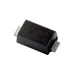
�SS13FL / SS14FL
Surface Mount Schottky Barrier Rectifier
Features
•
•
•
•
•
SOD-123F
Ultra Thin Profile – Maximum Height of 1.08 mm
UL Flammability 94V-0 Classification
MSL 1
RoHS Compliant / Green Mold Compound
Industrial Device Qualified per AEC-Q101 Standards.
* see authorized use policy
Band Indicates Cathode
1
2
Cathode
Anode
Ordering Information
Part Number
Top Mark
Package
Packing Method
SS13FL
G3
SOD-123F
Tape and Reel
SS14FL
G4
SOD-123F
Tape and Reel
Absolute Maximum Ratings
Stresses exceeding the absolute maximum ratings may damage the device. The device may not function or be operable above the recommended operating conditions and stressing the parts to these levels is not recommended. In addition, extended exposure to stresses above the recommended operating conditions may affect device reliability. The
absolute maximum ratings are stress ratings only. Values are at TA = 25°C unless otherwise noted.
Symbol
VRRM
VR
IF(AV)
IFSM
TJ
TSTG
Parameter
Value
SS13FL
SS14FL
Peak Reverse Voltage
30
40
Reverse Voltage
30
40
Unit
V
V
Average Rectified Current at TA = 75°C
1.0
A
Non-Repetitive Peak Forward Surge Current at t = 8.3 ms
40
A
Operating Junction Temperature Range
-55 to +125
°C
Storage Temperature Range
-55 to +125
°C
© 2015 Fairchild Semiconductor Corporation
SS13FL / SS14FL Rev. 1.1
www.fairchildsemi.com
SS13FL / SS14FL — Surface Mount Schottky Barrier Rectifier
August 2015
�Values are at TA = 25°C unless otherwise noted.
Symbol
Parameter
Value
ψJL
Typical Thermal Characteristics, Junction-to-Lead
RθJA
Typical Thermal Resistance, Junction-to-Ambient
(2)
Unit
25
°C/W
140
°C/W
Note:
1. Per JESD51-3 recommended thermal test board. Device mounted on FR-4 PCB, board size = 76.2 mm x 114.3 mm.
2. Thermocouple soldered at cathode lead.
Electrical Characteristics
Values are at TA = 25°C unless otherwise noted.
Symbol
Parameter
BVR
Reverse Breakdown Voltage
IR = 500 μA
VF
Forward Voltage
IF = 1.0 A
IR
Reverse Leakage Current
VR = VRRM
Trr
Reverse Recovery Time
IF = 0.5 A, IR = 1 A,
Irr = 0.25 A
CJ
Junction Capacitance
VR = 0
© 2015 Fairchild Semiconductor Corporation
SS13FL / SS14FL Rev. 1.1
Conditions
Min.
SS13FL
30
SS14FL
40
Typ.
Max.
Unit
V
SS13FL
5.875
SS14FL
5.695
60
0.55
V
30
μA
ns
pF
www.fairchildsemi.com
2
SS13FL / SS14FL — Surface Mount Schottky Barrier Rectifier
Thermal Characteristics(1)
�AVERAGE FORWARD RECTIFIED
CURRENT AMPERES
10 4
1
REVERSE CURRENT , m A
O
0.75
0.5
SINGLE PHASE HALF WAVE 60Hz
RESTSTIVE OR INDUCTIVE LOAD
P.C.B MOUNTED
,,
ON 0.2x0.2 (5.0x5.0mm)
COPPER PAD AREAS
0.25
0
0
25
50
75
100
125
150
125 C
10
3
10
2
75 OC
10
O
25 C
1
0.1
0
175
20
O
Figure 2. Typical Reverse Characteristic
Figure 1. Forward Current Derating Curve
INSTANTANEOUS FORWARD CURRENT,
AMPERES
CAPACITANCE,(pF )
1000
20 - 40V
60V
100V
10
O
T J=25 C
0.1
0
10
20
30
20
20-40V
10
60V
100V
1.0
O
TJ = 25 C
PulseWidth= 300ms
1%Duty Cycle
0.1
.5
40
V R, REVERSE VOLTAGE(VOLTS)
.7
.8
.9 1.1 1.3 1.5 1.7 1.9
INSTANTANEOUS FORWARD VOLTAGE,VOLTS
Figure 3. Typical Junction Characteristic
© 2015 Fairchild Semiconductor Corporation
SS13FL / SS14FL Rev. 1.1
60
REVERSE VOLTAGE ,V R(V)
LEAD TEMPERATURE , C
100
40
Figure 4. Typical Instantaneous Forward
Characteristics
www.fairchildsemi.com
3
SS13FL / SS14FL — Surface Mount Schottky Barrier Rectifier
Typical Performance Characteristics
�����
����
����
����
����
����
����
����
����
����
����
����
/$1'�3$77(51�5(&200(1'$7,21
� ���
����
����
����
����
$
������� $
127(6�
��$��7+,6�3$&.$*(�'2(6�127�&21)250�72�
�������$1