Ordering number : ENA2284A
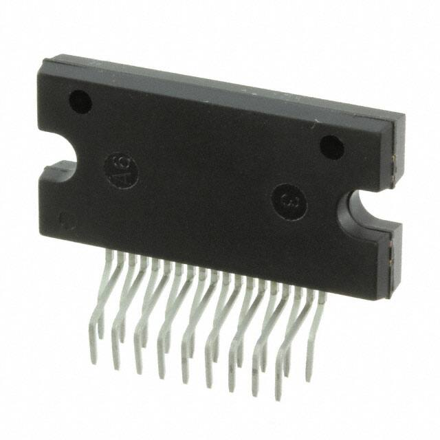
STK672-740AN-E
Thick-Film Hybrid IC
2-phase Stepper Motor Driver
http://onsemi.com
Overview
The STK672-740AN-E is a hybrid IC for use as a unipolar, 2-phase stepper motor driver with PWM current control.
Applications
Office photocopiers, printers, etc.
Features
Built-in overcurrent detection function, overheat detection function (output current OFF).
FAULT signal (active low) is output when overcurrent or overheat is detected.
Built-in power on reset function.
Phase signal input driver activated with an active Low and incorpororates a simulataneous ON prevention function.
Supports schmitt input for 2.5V high level input.
Incorporating a current detection resistor (0.089Ω: resistor tolerance 2%), motor current can be set using two
external resistors.
The ENABLE pin can be used to cut output current while maintaining the excitation mode.
Supports compatible pins with STK672-732AN-E.
Specifications
Absolute Maximum Ratings at Tc = 25C
Ratings
Unit
Maximum supply voltage 1
Parameter
VCC max
Symbol
No signal
Conditions
52
V
Maximum supply voltage 2
VDD max
No signal
0.3 to 6.0
V
Input voltage
Vin max
Logic input pins
0.3 to 6.0
V
Output current 1
IOP max
10μs 1 pulse (resistance load)
20
A
Output current 2
IOH max
VDD = 5V, More than 200Hz
4.0
A
Output current 3
IOF max
16pin Output current
10
mA
Allowable power dissipation 1
PdMF max
With an arbitrarily large heat sink. Per MOSFET
8.3
W
Allowable power dissipation 2
PdPK max
No heat sink
3.1
W
Operating substrate temperature
Tcmax
105
°C
Junction temperature
Tjmax
150
°C
Storage temperature
Tstg
40 to 125
°C
Stresses exceeding those listed in the Maximum Ratings table may damage the device. If any of these limits are exceeded, device functionality should not be assumed,
damage may occur and reliability may be affected.
ORDERING INFORMATION
See detailed ordering and shipping information on page 26 of this data sheet.
Semiconductor Components Industries, LLC, 2014
March, 2014 Ver. 2.2a
30614HK/11714HK 018-13-0068 No.2284-1/26
�STK672-740AN-E
Allowable Operating Ranges at Tc=25C
Parameter
Symbol
Conditions
Ratings
unit
Operating supply voltage 1
VCC
With signals applied
0 to 42
V
Operating supply voltage 2
VDD
With signals applied
55%
V
Input high voltage
VIH
Pins 10, 12, 13, 14, 15, 17, VDD=55%
2.5 to VDD
V
Input low voltage
VIL
Pins 10, 12, 13, 14, 15, 17, VDD=55%
0 to 0.8
V
3.0
A
3.3
A
0 to 105
C
0.14 to 1.31
V
Output current 1
IOH1
Output current 2
IOH2
Tc=105C, More than 200Hz ,
Continuous operation, duty=100%
Tc=80C, More than 200Hz,
Continuous operation, duty=100%,
See the motor current (IOH) derating curve
Recommended operating
substrate temperature
Recommended Vref range
Tc
No condensation
Vref
Tc=105C
Functional operation above the stresses listed in the Recommended Operating Ranges is not implied. Extended exposure to stresses beyond the Recommended
Operating Ranges limits may affect device reliability.
Electrical Characteristics at Tc=25C, VCC=24V, VDD=5.0V *1
Parameter
VDD supply current
Symbol
Conditions
min
ICCO
VDD=5.0V, ENABLE=Low
Output average current *2
Ioave
R/L=1/0.62mH in each phase
FET diode forward voltage
Vdf
If=1A (RL=23)
Output saturation voltage
Vsat
RL=23
Input high voltage
VIH
Pins 10, 12, 13, 14, 15, 17
2.5
Control
Input low voltage
VIL
Pins 10, 12, 13, 14, 15, 17
0.3
Input pin
5V level input current
IILH
Pins 10, 12, 13, 14, 15, 17=5V
GND level input current
IILL
Pins 10, 12, 13, 14, 15, 17=GND
FAULT
Output low voltage
VOLF
Pin 16 (IO=5mA)
pin
5V level leakage current
IILF
Pin 16 =5V
IIB
Pin 19 =1.0V
Vref input bias current
PWM frequency
Fc
Overheat detection temperature
TSD
Design guarantee
Drain-source cut-off current
IDSS
VDS=100V, Pins 2, 6, 9, 18=GND
0.519
29
typ
max
unit
4.4
8.0
mA
0.625
0.731
0.83
1.5
V
0.20
0.33
V
VDD
V
A
0.8
V
50
75
A
10
A
0.25
0.5
V
10
A
10
15
A
45
61
kHz
1
A
C
144
Notes
*1: A fixed-voltage power supply must be used.
*2: The value for Ioave assumes that the lead frame of the product is soldered to the mounting circuit board.
Product parametric performance is indicated in the Electrical Characteristics for the listed test conditions, unless otherwise noted. Product performance may not be
indicated by the Electrical Characteristics if operated under different conditions.
No.2284-2/26
�STK672-740AN-E
Derating Curve of Motor Current, IOH, vs. STK672-740AN-E Operating Substrate Temperature, Tc
4.5
4
MOter Current IOH
A
3.5
3
200Hz 2ex
Hold
2.5
2
1.5
1
0.5
0
0
10
20
30
40
50
60
70
80
90
100
110
Operation substrate temperature Tc °C
Notes
The current range given above represents conditions when output voltage is not in the avalanche state.
If the output voltage is in the avalanche state, see the allowable avalanche energy for STK672-7** series hybrid ICs
given in a separate document.
The operating substrate temperature, Tc, given above is measured while the motor is operating.
Because Tc varies depending on the ambient temperature, Ta, the value of IOH, and the continuous or intermittent
operation of IOH, always verify this value using an actual set.
The Tc temperature should be checked in the center of the metal surface of the product package.
No.2284-3/26
�STK672-740AN-E
Block Diagram
VDD=5V
φBB
9
10
N.C
11
φAB
17
φB
12
φA
13
RESETB 14
N.C
N.C
A
AB
B
BB
8
4
5
7
3
1
VDD
F1
BBIN
16
F3
F4
FAB
BIN
FBO
ABIN
FBB
AIN
Latch
circuit
Over
current
R1
R2
Power on reset
ENABLE 15
FAULT
F2
FAO
Over heating
detection
AI
Current control
Chopper circuit
FAULT signal
(Open drain)
Vref/4.9
Latch
circuit
Vref
Amplifier
VSS
100k
2
P.G2
6
P.G1
BI
VSS
VSS
S.G
18
Vref
19
No.2284-4/26
�STK672-740AN-E
Measurement Circuit
(The terminal which is not appointed is open. The measurement circuit of STK672-740AN-E is the same as
STK672-732AN-E.)
24V
1. Vdf
23Ω
13
9
V
6
2
Vdf
5
17
7
12
3
10
1
15
14
STK672-
19
74xAN-E
16
18
GND
2. IILF,IILH,IILL,IIB
3. Vsat
5V
5V
5V
1V
10
IILL
15
16
A
19
7
12
7
3
10
3
15
1
5V
14
STK67274xAN-E
18 2
23Ω
5
1
14
IIB
9
17
5
12
A
24V
13
17
IILH
GND
9
13
IILF
10k
19
STK67274xAN-E
16 18 2
6
V
Vsat
6
GND
GND
4. Icco, Ioave, fc,VOLF
Icco
5V
A
9
13
17
10
3
15
1
14
7.5K
STK672-
0.62mH
1Ω
24V
Ioave
74xAN-E
19
16 18 2
1K
Ioave
7
12
910
5
VOLF
6
+
SW
100μ
Close SW at
fc
mesurement of VOLF
GND
No.2284-5/26
�STK672-740AN-E
Sample Application Circuit
2 phase stepper motor driver
9
VDD(5V)
ΦA
13
ΦAB
17
ΦB
12
ΦBB
10
ENABLE
15
RESETB
R01
14
R03
FAULT
5
7
3
STK672
-74xAN-E
+
Vref
VCC
24V
B
BB
+
C01
at least 100F
16
C02
10F
1
A
AB
2
19
18
R02
6
P.G2
P.G1
P.GND
S.G
Precautions
[GND wiring]
To reduce noise on the 5V/24V system, be sure to place the GND of C01 in the circuit given above as close as possible
to Pin 2 and Pin 6 of the hybrid IC.
In addition, in order to set the current accurately, the GND side of RO2 of Vref must be connected to the shared ground
terminal used by the Pin 18 (S.G) GND, P.G1 and P.G2.
[Input pins]
If VDD is being applied, use care that each input pin does not apply a negative voltage less than -0.3V to S. GND,
Pin 18. Measures must also be taken so that a voltage equal to or greater than VDD is not input.
Do not wire by connecting the circuit pattern on the P.C.B side to Pins 4, 8, or 11 on the N.C. shown in the internal
block diagram.
Apply 2.5V high level input to pins 10, 12, 13, 14, 15, and 17.
Since the input pins do not have built-in pull-up resistors, when the open-collector type pins 10, 12, 13, 14, 15, and 17
are used as inputs, a 1 to 20k pull-up resistor (to VDD) must be used.
At this time, use a device for the open collector driver that has output current specifications that pull the voltage down to
less than 0.8V at Low level (less than 0.8V at Low level when IOL=5mA).
[Current setting Vref]
Considering the specifications for the Vref input bias current IIB, we recommend a value 1k or less for R02.
If the motor current is temporarily reduced, the circuit given below(STK672-740AN: IOH>0.3A) is recommended.
R3
5V
5V
R01
Vref
R01
R02
Vref
R3
R02
No.2284-6/26
�STK672-740AN-E
[Setting the motor current]
The motor current, IOH, is set using the Pin 19 voltage, Vref, of the hybrid IC.
Equations related to IOH and Vref are given below.
Vref (RO2 (RO2+RO1))VDD(5V) ··········································· (1)
IOH (Vref 4.9) Rs ······························································· (2)
The value of 4.9 in Equation (2) above represents the Vref voltage as divided by a circuit inside the control IC.
Rs : 0.089 (Current detection resistor inside the hybrid IC)
IOH
0
[Smoke Emission Precuations]
If Pin 18 (S.G terminal) is attached to the board without using solder, overcurrent may flow into the MOSFET at VCCON
(24V ON), causing the STK672-740AN-E to emit smoke because 5V circuits cannot be controlled.
In addition, as long as one of the output Pins, 1, 3, 5, or 7, is open, inductance energy stored in the motor results in
electrical stress on the driver, possibly resulting in the emission of smoke.
Input Pin Functions
Pin Name
Pin No.
Function
Input Conditions When Operating
ΦA
13
Phase signal input of 5pin (phase A output).
ΦAB
17
Phase signal input of 7pin (phase AB output).
Low active(with a function to prevent simultaneous ON
ΦB
12
Phase signal input of 3pin (phase B output).
of ΦA and ΦAB ,or ΦB and ΦBB.
ΦBB
10
Phase signal input of 1pin (phase BB output).
RESETB
14
System reset
Initial state of A and BB phase excitation in the timing charts
A reset is applied by a low level
is set by switching from low to high.
The A, AB, B, and BB outputs are turned off, and after
ENABLE
15
operation is restored by returning the ENABLE pin to the
The A, AB, B, and BB outputs are turned off by a
high level, operation continues with the same excitation
low-level input.
timing as before the low-level input.
Output Pin Functions
Pin Name
FAULT
Pin No.
16
Function
Monitor pin used when over-current detection or overheat
detection function is activated.
Input Conditions When Operating
Low level is output when detected.
Note : See the timing chart for the concrete details on circuit operation.
No.2284-7/26
�STK672-740AN-E
Timing Charts
2-phase excitation
VDD
Power on reset
(or RESETB)
φA
φAB
φB
φBB
ENABLE
FAO
FAB
FBO
FBB
1-2 phase excitation
VDD
Power on reset
(or RESETB)
φA
φAB
φB
φBB
ENABLE
FAO
FAB
FBO
FBB
No.2284-8/26
�STK672-740AN-E
1-2 phase excitation (ENABLE)
VDD
Power on reset
(or RESETB)
φA
φAB
φB
φBB
ENABLE
FAO
Output off
FAB
FBO
FBB
1-2 phase excitation (Hold operation results during fixed CLOCK)
VDD
Power on reset
(or RESETB)
φA
φAB
φB
φBB
ENABLE
FAO
Hold operation
FAB
FBO
FBB
No.2284-9/26
�STK672-740AN-E
Package Dimensions
unit : mm
SIP19 29.2x14.4
CASE 127CF
ISSUE O
1
19
No.2284-10/26
�STK672-740AN-E
STK672-740AN-E
Technical data
1.
2.
3.
4.
5.
6.
7.
8.
Input Pins and Functional Overview
STK672-740AN-E over current detection, thermal shutdown detection.
STK672-740AN-E Allowable Avalanche Energy
STK672-740AN-E Internal Loss Calculation
Thermal Design
Package Power Loss PdPK Derating Curve for the Ambient Temperature Ta
Example of Stepper Motor Driver Output Current Path (1-2 phase excitation)
Other usage notes
No.2284-11/26
�STK672-740AN-E
1. I/O Pins and Functions of the Control Block
[Pin description]
HIC pin
Pin Name
14
RESETB
Function
System reset
15
ENABLE
Motor current OFF
16
FAULT
19
Vref
Overcurrent/over-heat detection output
Current value setting
Description of each pin
1-1.[RESETB (System-wide reset)]
The reset signal is formed by the power-on reset function built into the HIC and the RESETB terminal.
When activating the internal circuits of the HIC using the power-on reset signal within the HIC, be sure to connect Pin
14 of the HIC to VDD.
1-2. [ENABLE (Forcible OFF control of excitation drive output A, AB, B, and BB, and selecting operation/hold status
inside the HIC)]
ENABLE=1: Normal operation
When ENABLE=0: Motor current goes OFF, and excitation drive output is forcibly turned OFF.
The system clock inside the HIC stops at this time, with no effect on the HIC even if input pins other than RESET input
vary. In addition, since current does not flow to the motor, the motor shaft becomes free.
If the A to BB signal input used for motor rotation suddenly stops, the motor shaft may advance beyond the control
position due to inertia. A SLOW DOWN setting where the A to BB signal input cycle gradually decreases is
required in order to stop at the control position.
1-3. [FAULT]
FAULT is an open drain output. It outputs low level when overcurrent, or overheat is detected.
1-4. [Vref (Voltage setting to be used for the current setting reference)]
Input voltage is in the voltage range of 0.14V to 1.31V.
The recommended Vref voltage is 0.14V or higher because the output offset voltage of Vref/4.9 amplifier cannot be
controlled down to 0V.
Note:Pin type is analog input configuration and input pull-down resistance 100 k.
The internal impedance 100 k is designed so that the increase in current is prevented while Pin 19 is open.
1-5. [Input timing]
The control IC of the driver is equipped with a power on reset function capable of initializing internal IC operations
when power is supplied. A 4V typ setting is used for power on reset. Because the specification for the MOSFET gate
voltage is 5V5%, conduction of current to output at the time of power on reset adds electromotive stress to the
MOSFET due to lack of gate voltage. To prevent electromotive stress, be sure to set ENABLE=Low while VDD,
which is outside the operating supply voltage, is less than 4.75V.
Control IC power (VDD) rising edge
4Vtyp
3.8Vtyp
Control IC power on reset
RESETB signal input
No time specification
ENABLE signal input
ΦA to ΦBB signal input
No time specification
No time specification
RESETB, ENABLE, A to BB Signals Input Timing
No.2284-12/26
�STK672-740AN-E
1-6. [Configuration of control block I/O pins]
Input pins 13,17,12,10,15,14pin
VDD
10kΩ
Input pin
100kΩ
VSS
The input pins of this driver all use Schmitt input. Typical specifications at Tc=25C are given below. Hysteresis
voltage is 0.3V (VIHa-VILa).
When rising
When falling
1.8Vtyp
1.5Vtyp
Input voltage
VIHa
VILa
Input voltage specifications are as follows.
VIH=2.5Vmin
VIL=0.8Vmax
VDD
Output pin
Pin16
Vref /4.9
Overcurrent
Amplif ier
100kΩ
VSS
VSS
Overheating
Input pin
Pin19
VSS
No.2284-13/26
�STK672-740AN-E
2. Overcurrent detection, overheat detection functions
Each detection function operates using a latch system and turns output off. Because a RESET signal is required to
restore output operations, once the power supply, VDD, is turned off, you must either again apply power on reset with
VDDON or apply a RESETB=HighLowHigh signal.
2-1.[Overcurrent detection]
This hybrid IC is equipped with a function for detecting overcurrent that arises when the motor burns out or when there
is a short between the motor terminals.
Overcurrent detection occurs at 3.5A typ with the STK672-732AN-E, and 5.5A typ with the STK672-740AN-E.
Current when motor terminals are shorted
PWM period
Overcurrent detection
IOHmax
Set motor
current, IOH
MOSFET all OFF
No detection interval
(5.5s typ)
Normal operation
5.5s typ
Operation when motor pins are shorted
Overcurrent detection begins after an interval of no detection (a dead time of 5.5s typ) during the initial ringing part
during PWM operations. The no detection interval is a period of time where overcurrent is not detected even if the
current exceeds IOH.
2-2. [Overheat detection]
Rather than directly detecting the temperature of the semiconductor device, overheat detection detects the temperature
of the aluminum substrate (144C typ).
Within the allowed operating range recommended in the specification manual, if a heat sink attached for the purpose of
reducing the operating substrate temperature, Tc, comes loose, the semiconductor can operate without breaking.
However, we cannot guarantee operations without breaking in the case of operations other than those recommended,
such as operations at a current exceeding IOH max that occurs before overcurrent detection is activated.
No.2284-14/26
�STK672-740AN-E
3. Allowable Avalanche Energy Value
(1) Allowable Range in Avalanche Mode
When driving a 2-phase Stepper motor with constant current chopping using an STK672-7** Series hybrid IC, the
waveforms shown in Figure 1 below result for the output current, ID, and voltage, VDS.
VDSS: Voltage during avalanche operations
IOH: Motor current peak value
IAVL: Current during avalanche operations
tAVL: Time of avalanche operations
Figure 1 Output Current, ID, and Voltage, VDS, Waveforms 1 of the STK672-7** Series when Driving a
2-Phase Motor with Constant Current Chopping
When operations of the MOSFET built into STK672-7** Series ICs is turned off for constant current chopping, the ID
signal falls like the waveform shown in the figure above. At this time, the output voltage, VDS, suddenly rises due to
electromagnetic induction generated by the motor coil.
In the case of voltage that rises suddenly, voltage is restricted by the MOSFET VDSS. Voltage restriction by VDSS
results in a MOSFET avalanche. During avalanche operations, ID flows and the instantaneous energy at this time, EAVL1,
is represented by Equation (3-1).
EAVL1=VDSSIAVL0.5tAVL ------------------------------------------- (3-1)
VDSS: V units, IAVL: A units, tAVL: sec units
The coefficient 0.5 in Equation (3-1) is a constant required to convert the IAVL triangle wave to a square wave.
During STK672-7** Series operations, the waveforms in the figure above repeat due to the constant current chopping
operation. The allowable avalanche energy, EAVL, is therefore represented by Equation (3-2) used to find the average
power loss, PAVL, during avalanche mode multiplied by the chopping frequency in Equation (3-1).
PAVL=VDSSIAVL0.5tAVLfc -------------------------------- (3-2)
fc: Hz units (fc is set to the PWM frequency of 50kHz.)
For VDSS, IAVL, and tAVL, be sure to actually operate the STK672-7** Series and substitute values when operations
are observed using an oscilloscope.
Ex. If VDSS=110V, IAVL=1A, tAVL=0.2s, the result is:
PAVL=11010.50.210-650103=0.55W
VDSS=110V is a value actually measured using an oscilloscope.
The allowable loss range for the allowable avalanche energy value, PAVL, is shown in the graph in Figure 3.
When examining the avalanche energy, be sure to actually drive a motor and observe the ID, VDSS, and tAVL waveforms
during operation, and then check that the result of calculating Equation (3-2) falls within the allowable range for
avalanche operations.
No.2284-15/26
�STK672-740AN-E
(2) ID and VDSS Operating Waveforms in Non-avalanche Mode
Although the waveforms during avalanche mode are given in Figure 1, sometimes an avalanche does not result during
actual operations.
Factors causing avalanche are listed below.
Poor coupling of the motor’s phase coils (electromagnetic coupling of A phase and AB phase, B phase and BB phase).
Increase in the lead inductance of the harness caused by the circuit pattern of the board and motor.
Increases in VDSS, tAVL, and IAVL in Figure 1 due to an increase in the supply voltage from 24V to 36V.
If the factors above are negligible, the waveforms shown in Figure 1 become waveforms without avalanche as shown
in Figure 2.
Under operations shown in Figure 2, avalanche does not occur and there is no need to consider the allowable loss
range of PAVL shown in Figure 3.
IOH: Motor current peak value
Figure 2 Output Current, ID, and Voltage, VDS, Waveforms 2 of the STK672-7** Series when Driving
a 2-Phase Stepper Motor with Constant Current Chopping
5
4.5
4
3.5
3
PAVL W
Average power loss PAVL during avalanche
Figure 3 Allowable Loss Range, PAVL-IOH During STK672-740AN-E Avalanche Operations
PAVL-IOH
Tc=105°C
Tc=80°C
2.5
2
1.5
1
0.5
0
0
1
2
3
4
Motor current, IOH A
Note :
The operating conditions given above represent a loss when driving a 2-phase stepper motor with constant current
chopping.
Because it is possible to apply 3W or more at IOH=0A, be sure to avoid using the MOSFET body diode that is used to
drive the motor as a zener diode.
No.2284-16/26
�STK672-740AN-E
4. Calculating STK672-740AN-E HIC Internal Power Loss
The average internal power loss in each excitation mode of the STK672-740AN-E can be calculated from the following
formulas. *1
Each excitation mode
2-phase excitation mode
2PdAVex=(Vsat+Vdf) (1/(t1+t2+t3)) IOHt2+(1/(t1+t2+t3)) IOH(Vsatt1+Vdft3)
1-2 Phase excitation mode
1-2PdAVex=(Vsat+Vdf) (1/(t1+t2+t3)) IOHt2+(1/(t1+t2+t3)) IOH(Vsatt1+Vdft3)
Motor hold mode
HoldPdAVex= (Vsat+Vdf) IOH
Vsat : Combined voltage represented by the Ron voltage drop+shunt resistor
Vdf : Combined voltage represented by the MOSFET body diode+shunt resistor
t1, t2, and t3 represent the waveforms shown in the figure below.
t1 : Time required for the winding current to reach the set current (IOH)
t2 : Time in the constant current control (PWM) region
t3 : Time from end of phase input signal until inverse current regeneration is complete
IOH
0A
t1
t2
t3
Motor COM Current Waveform Model
t1= (-L/(R+0.20)) ln (1-(((R+0.20)/VCC) IOH))
t3= (-L/R) ln ((VCC+0.20)/(IOHR+VCC+0.20))
VCC : Motor supply voltage (V)
L
: Motor inductance (H)
R
: Motor winding resistance ()
IOH : Motor set output current crest value (A)
For the values of Vsat and Vdf, be sure to substitute from Vsat vs IOH and Vdf vs IOH at the setting current value IOH.
(See pages to follow)
Then, determine if a heat sink is necessary by comparing with the Tc vs Pd graph (see next page) based on the
calculated average output loss, HIC.
For heat sink design, be sure to see ‘5. Thermal Design’.
The HIC average power, PdAVex described above, represents loss when not in avalanche mode.
To add the loss in avalanche mode, be sure to add PAVL using the formula (for average power loss , PAVL, for
STK672-7** during avalanche mode, described below to PdAVex described above.)
When using this IC without a fin, always check for temperature increases in the set, because the HIC substrate
temperature, Tc, varies due to effects of convection around the HIC.
No.2284-17/26
�STK672-740AN-E
4-2. [Calculating the average power loss, PAVL, during avalanche mode]
The allowable avalanche energy, EAVL, during fixed current chopping operation is represented by Equation (3-2) used
to find the average power loss, PAVL, during avalanche mode that is calculated by multiplying Equation (3-1) by the
chopping frequency.
PAVL=VDSSIAVL0.5tAVLfc ············································································· (3-2)
fc : Hz units (fc is set to the PWM frequency of 50kHz.)
Be sure to actually operate an STK672-7** series and substitute values found when observing operations on an
oscilloscope for VDSS, IAVL, and tAVL.
The sum of PAVL values for each excitation mode is multiplied by the constants given below and added to the average
internal HIC loss equation, except in the case of 2-phase excitation.
1-2 excitation mode and higher: PAVL(1)=0.7PAVL ························································(4-1)
During2-phase excitation mode and motor hold: PAVL(1)=1PAVL ·······································(4-2)
No.2284-18/26
�STK672-740AN-E
Output Saturation Voltage Vsat - V
STK672-740AN-E Output Saturation Voltage Vsat vs. Output Current
1
0.8
0.6
Tc=25°C
Tc=105°C
0.4
0.2
0
0
0.5
1
1.5
2
2.5
3
3.5
4
4.5
Output current, IOH - A
STK672-740AN-E Forward voltage, Vdf -Output current, IOH
Forward voltage, Vdf - V
1.4
1.2
1
0.8
Tc=25°C
0.6
Tc=105°C
0.4
0.2
0
0
0.5
1
1.5
2
2.5
3
3.5
4
4.5
Output current, IOH - A
Substrate temperature rise, Tc (no heat sink) - Internal average power dissipation,
Substrate temperature rise, Tc - C
PdAV
80
70
60
50
40
30
20
10
0
0
0.5
1
1.5
2
2.5
3
3.5
Hybrid IC internal average power dissipation, PdAV - W
No.2284-19/26
�STK672-740AN-E
5. Thermal design
[Operating range in which a heat sink is not used]
Use of a heat sink to lower the operating substrate temperature of the HIC (Hybrid IC) is effective in increasing the
quality of the HIC.
The size of heat sink for the HIC varies depending on the magnitude of the average power loss, PdAV, within the HIC.
The value of PdAV increases as the output current increases. To calculate PdAV, refer to “Calculating Internal HIC
Loss” in the specification document.
Calculate the internal HIC loss, PdAV, assuming repeat operation such as shown in Figure 1 below, since
conduction during motor rotation and off time both exist during actual motor operations,
IO1
Motor phase current
(sink side)
IO2
0A
-IO1
T1
T2
T3
T0
Figure 1 Motor Current Timing
T1 : Motor rotation operation time
T2 : Motor hold operation time
T3 : Motor current off time
T2 may be reduced, depending on the application.
T0 : Single repeated motor operating cycle
IO1 and IO2 : Motor current peak values
Due to the structure of motor windings, the phase current is a positive and negative current with a pulse form.
Note that figure 1 presents the concepts here, and that the on/off duty of the actual signals will differ.
The hybrid IC internal average power dissipation PdAV can be calculated from the following formula.
PdAV= (T1P1+T2P2+T30) TO ---------------------------- (I)
(Here, P1 is the PdAV for IO1 and P2 is the PdAV for IO2)
If the value calculated using Equation (I) is 1.5W or less, and the ambient temperature, Ta, is 60C or less, there is no
need to attach a heat sink. Refer to Figure 2 for operating substrate temperature data when no heat sink is used.
[Operating range in which a heat sink is used]
Although a heat sink is attached to lower Tc if PdAV increases, the resulting size can be found using the value of
c-a in Equation (II) below and the graph depicted in Figure 3.
c-a= (Tc max-Ta) PdAV ---------------------------- (II)
Tc max : Maximum operating substrate temperature =105C
Ta: HIC ambient temperature
Although a heat sink can be designed based on equations (I) and (II) above, be sure to mount the HIC in a set and
confirm that the substrate temperature, Tc, is 105C or less.
The average HIC power loss, PdAV, described above represents the power loss when there is no avalanche operation.
To add the loss during avalanche operations, be sure to add Equation (3-2), “Allowable STK672-7** Avalanche
Energy Value”, to PdAV.
No.2284-20/26
�STK672-740AN-E
Figure 2
Substrate temperature rise, Tc (no heat sink) - Internal average power dissipation,
Substrate temperature rise, Tc - C
PdAV
80
70
60
50
40
30
20
10
0
0
0.5
1
1.5
2
2.5
3
3.5
Hybrid IC internal average power dissipation, PdAV - W
Figure 3
Heat sink area (Board thickness: 2mm) - c-a
Heat sink thermal resistance,
Θc -a- C / W
100
No surface finish
Surface finished in
black
10
1
10
100
1000
Heat sink area, S cm2 (thickness : 2mm)
No.2284-21/26
�STK672-740AN-E
6. Mitigated Curve of Package Power Loss, PdPK, vs. Ambient Temperature, Ta
Package power loss, PdPK, refers to the average internal power loss, PdAV, allowable without a heat sink.
The figure below represents the allowable power loss, PdPK, vs. fluctuations in the ambient temperature, Ta.
Power loss of up to 3.1W is allowable at Ta=25C, and of up to 1.75W at Ta=60C.
* The package thermal resistance θc-a is 25.8°C/W.
Allowable power dissipation, PdPK (no heat sink) - Ambient temperature, Ta
Allowable power dissipation, PdPK - W
3.5
3
2.5
2
1.5
1
0.5
0
0
20
40
60
80
100
120
Ambient temperature, Ta - °C
No.2284-22/26
�STK672-740AN-E
7. Example of Stepper Motor Driver Output Current Path (1-2 phase excitation)
2 Phase stepper motor
IoA
VDD
IoAB
A
AB
B
BB
F1
F2
F3
F4
FAO
BBIN
Vcc
FAB
FBO
FBB
BIN
ABIN
24V
AIN
RESETB
ENABLE
FAULT
Latch
Power on
reset
R1
AI
BI
Chopper
circuit
FAULT signal
(Open drain)
Over heat
detection
Over
current
detection
Vref
/4.9
Latch
Vref
Amp
100k
VSS
+ C02
R2
P.G2
at least 100F
P.GND
P.G1
VSS
VSS
φA(Pin 13)
φAB(Pin 17)
Phase A output
current
IoA
PWM operation
Phase AB output
current
IoAB
When PWM operations of IOA
are OFF, for IOAB, negative
current flows through the
parasitic diode, F2.
When PWM operations of IOAB
are OFF, for IOA, negative
current flows through the
parasitic diode, F1.
No.2284-23/26
�STK672-740AN-E
8. Other usage notes
In addition to the “Notes” indicated in the Sample Application Circuit, care should also be given to the following
contents during use.
(1) Allowable operating range
Operation of this product assumes use within the allowable operating range. If a supply voltage or an input voltage
outside the allowable operating range is applied, an overvoltage may damage the internal control IC or the
MOSFET.
If a voltage application mode that exceeds the allowable operating range is anticipated, connect a fuse or take other
measures to cut off power supply to the product.
(2) Input pins
If the input pins are connected directly to the board connectors, electrostatic discharge or other overvoltage outside
the specified range may be applied from the connectors and may damage the product. Current generated by this
overvoltage can be suppressed to effectively prevent damage by inserting 100 to 1k resistors in lines connected
to the input pins.
Take measures such as inserting resistors in lines connected to the input pins.
(3) Power connectors
If the motor power supply VCC is applied by mistake without connecting the GND part of the power connector
when the product is operated, such as for test purposes, an overcurrent flows through the VCC decoupling capacitor,
C1, to the parasitic diode between the VDD of the internal control IC and GND, and may damage the power supply
pin block of the internal control IC.
To prevent damage in this case, connect a 10 resistor to the VDD pin, or insert a diode between the VCC
decoupling capacitor C1 GND and the VDD pin.
Overcurrent protection measure: insert a resistor
VDD=5V
5V
Reg.
.
9
A
AB
B
BB
5
7
3
1
VDD
FAO
FABO
ΦA
FBO
ΦAB
Vcc
FBBO
ΦB
ΦBB
R1
ENABLE
AI
RESETB
BI
R2
GND
2
6
Vref
FAULT
Vref
24V
Reg
.
C1
VSS
S.G
open
Overcurrent protection measure: insert a diode
Overcurrent path
(4) Input Signal Lines
1) Do not use an IC socket to mount the driver, and instead solder the driver directly to the board to minimize
fluctuations in the GND potential due to the influence of the resistance component and inductance component of
the GND pattern wiring.
2) To reduce noise caused by electromagnetic induction to small signal lines, do not design small signal lines (sensor
signal lines, and 5V or 3.3V power supply signal lines) that run parallel in close proximity to the motor output line
A (Pin 5), AB (Pin 7), B (Pin 3), or BB (Pin 1) phases.
No.2284-24/26
�STK672-740AN-E
(5) When mounting multiple drivers on a single board
When mounting multiple drivers on a single board, the GND design should mount a VCC decoupling capacitor, C1, for
each driver to stabilize the GND potential of the other drivers. The key wiring points are as follows.
24v
5V
9
Input
Signals
Motor
1
IC1
9
Input
Signals
IC2
9
Input
Signals
Motor
3
IC3
2
2
2
19 18
Motor
2
6
19 18
6
6
19 18
GND
GND
Short
Thick and short
Thick
(6) VCC operating limit
When the output (for example F1) of a 2-phase stepper motor driver is turned OFF, the AB phase back electromotive
force eab produced by current flowing to the paired F2 parasitic diode is induced in the F1 side, causing the output
voltage VFB to become twice or more the VCC voltage. This is expressed by the following formula.
VFB = VCC + eab
= VCC + VCC + IOH x RM + Vdf (1.5V)
VCC: Motor supply voltage, IOH: Motor current set by Vref
Vdf: Voltage drop due to F2 parasitic diode and current detection resistor R1, RM: Motor winding resistance value
Using the above formula, make sure that VFB is always less than the MOSFET withstand voltage of 100V. This is
because there is a possibility that operating limit of VCC falls below the allowable operating range of 42V, due to the
RM and IOH specifications.
VCC
VCC
AB phase
A phase
AB phase
A phase
eab
eab is generated by the
mutual induction M.
Current path
VFB
M
F2
OFF
F1
ON
R1
GND
VCC
eab
Current path
M
F2
OFF
F1
OFF
R1
GND
The oscillating voltage in excess of VFB is caused by LCRM (inductance, capacitor, resistor, mutual inductance)
oscillation that includes micro capacitors C, not present in the circuit. Since M is affected by the motor characteristics,
there is some difference in oscillating voltage according to the motor specifications. In addition, constant voltage drive
without constant current drive enables motor rotation at VCC 0V.
No.2284-25/26
�STK672-740AN-E
ORDERING INFORMATION
Device
STK672-740AN-E
Package
SIP-19
(Pb-Free)
Shipping (Qty / Packing)
15 / Tube
ON Semiconductor and the ON logo are registered trademarks of Semiconductor Components Industries, LLC (SCILLC). SCILLC owns the rights to a number
of patents, trademarks, copyrights, trade secrets, and other intellectual property. A listing of SCILLC’s product/patent coverage may be accessed at
www.onsemi.com/site/pdf/Patent-Marking.pdf. SCILLC reserves the right to make changes without further notice to any products herein. SCILLC makes no
warranty, representation or guarantee regarding the suitability of its products for any particular purpose, nor does SCILLC assume any liability arising out of the
application or use of any product or circuit, and specifically disclaims any and all liability, including without limitation special, consequential or incidental
damages. “Typical” parameters which may be provided in SCILLC data sheets and/or specifications can and do vary in different applications and actual
performance may vary over time. All operating parameters, including “Typicals” must be validated for each customer application by customer’s technical
experts. SCILLC does not convey any license under its patent rights nor the rights of others. SCILLC products are not designed, intended, or authorized for use
as components in systems intended for surgical implant into the body, or other applications intended to support or sustain life, or for any other application in
which the failure of the SCILLC product could create a situation where personal injury or death may occur. Should Buyer purchase or use SCILLC products for
any such unintended or unauthorized application, Buyer shall indemnify and hold SCILLC and its officers, employees, subsidiaries, affiliates, and distributors
harmless against all claims, costs, damages, and expenses, and reasonable attorney fees arising out of, directly or indirectly, any claim of personal injury or
death associated with such unintended or unauthorized use, even if such claim alleges that SCILLC was negligent regarding the design or manufacture of the
part. SCILLC is an Equal Opportunity/Affirmative Action Employer. This literature is subject to all applicable copyright laws and is not for resale in any manner.
PS No.2284-26/26
�