MURD530T4G,
SURD8530T4G,
SURD8530T4G-VF01
Switch-mode
Power�Rectifier
www.onsemi.com
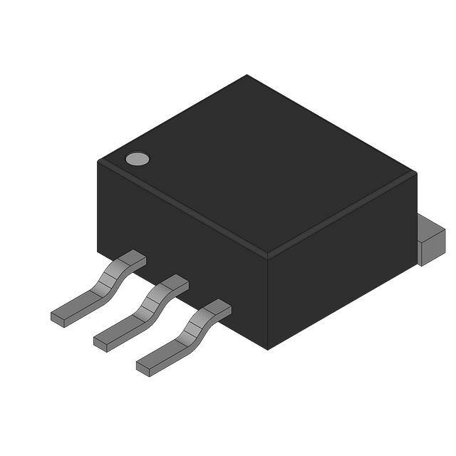
DPAK Surface Mount Package
These state−of−the−art devices are designed for use in switching
power supplies, inverters and as free wheeling diodes.
ULTRAFAST RECTIFIER
5.0 AMPERES, 300 VOLTS
Features
•
•
•
•
•
Ultrafast 50 Nanosecond Recovery Time
Low Forward Voltage Drop
Low Leakage
SURD8 Prefix for Automotive and Other Applications Requiring
Unique Site and Control Change Requirements; AEC−Q101
Qualified and PPAP Capable
These Devices are Pb−Free, Halogen Free/BFR Free and are RoHS
Compliant
DPAK
CASE 369C
1
MARKING DIAGRAM
Mechanical Characteristics
• Case: Epoxy, Molded
• Weight: 0.4 Gram (Approximately)
• Finish: All External Surfaces Corrosion Resistant and Terminal
•
Leads are Readily Solderable
Lead and Mounting Surface Temperature for Soldering Purposes:
260°C Max. for 10 Seconds
MAXIMUM RATINGS
Rating
Symbol
Value
Unit
Peak Repetitive Reverse Voltage
Working Peak Reverse Voltage
DC Blocking Voltage
VRRM
VRWM
VR
300
V
Average Rectified Forward Current
(Rated VR, TC = 165°C)
IF(AV)
Peak Repetitive Forward Current
(Rated VR, Square Wave,
20 kHz, TC = 165°C)
IFRM
Non−Repetitive Peak Surge Current
(Surge Applied at Rated Load
Conditions Halfwave, 60 Hz)
IFSM
Operating Junction and Storage
Temperature Range
TJ, Tstg
A
5.0
A
10
A
75
−65 to +175
°C
Stresses exceeding those listed in the Maximum Ratings table may damage the
device. If any of these limits are exceeded, device functionality should not be
assumed, damage may occur and reliability may be affected.
© Semiconductor Components Industries, LLC, 2015
June, 2017 − Rev. 6
1
4
3
AYWW
U
530G
U530
A
Y
WW
G
= Specific Device Number
= Assembly Location*
= Year
= Work Week
= Pb−Free Package
* The Assembly Location Code (A) is front side
optional. In cases where the Assembly Location is
stamped in the package bottom (molding ejecter
pin), the front side assembly code may be blank.
ORDERING INFORMATION
Package
Shipping†
MURD530T4G
DPAK
(Pb−Free)
2,500/Tape & Reel
16 mm
SURD8530T4G
DPAK
(Pb−Free)
2,500/Tape & Reel
16 mm
SURD8530T4G−
VF01
DPAK
(Pb−Free)
2,500/Tape & Reel
16 mm
Device
†For information on tape and reel specifications,
including part orientation and tape sizes, please
refer to our Tape and Reel Packaging Specifications
Brochure, BRD8011/D.
Publication Order Number:
MURD530/D
�MURD530T4G,
THERMAL CHARACTERISTICS
Characteristic
Symbol
Value
Unit
RqJC
3
°C/W
RqJA
92
°C/W
RqJA
57
°C/W
Symbol
Value
Unit
Thermal Resistance − Junction−to−Case (Note 1)
Thermal Resistance − Junction−to−Ambient (Note 2)
Thermal Resistance − Junction−to−Ambient (Note 3)
1. Rating applies for one diode leg.
2. Rating applies when for both diode legs when mounted on 130 mm2 pad size.
3. Rating applies for both diode legs when mounted on 1 in pad size.
ELECTRICAL CHARACTERISTICS
Characteristic
Maximum Instantaneous Forward Voltage Drop (Note 4)
(iF = 3 A, TJ = 25°C)
(iF = 3 A, TJ = 125°C)
(iF = 5 A, TJ = 25°C)
(iF = 5 A, TJ = 125°C)
vF
Maximum Instantaneous Reverse Current (Note 4)
(TJ = 25°C, Rated dc Voltage)
(TJ = 125°C, Rated dc Voltage)
iR
Maximum Reverse Recovery Time
(IF = 1 Amp, di/dt = 50 A/ms, VR = 30 V, TJ = 25°C)
trr
Volts
0.95
0.80
1.05
0.90
mA
5.0
150
ns
50
4. Pulse Test: Pulse Width = 300 ms, Duty Cycle ≤ 2.0%.
Product parametric performance is indicated in the Electrical Characteristics for the listed test conditions, unless otherwise noted. Product
performance may not be indicated by the Electrical Characteristics if operated under different conditions.
100
TJ = 175°C
85°C
125°C
1
25°C
−40°C
0.1
0
0.5
1.0
1.5
85°C
25°C
1
−40°C
0.1
2.0
125°C
0
0.5
1.0
1.5
vF, INSTANTANEOUS VOLTAGE (V)
Figure 1. Maximum Forward Voltage
Figure 2. Typical Forward Voltage
125°C
10
85°C
1.0
25°C
0.1
0.01
−40°C
0.001
50
2.0
1000
175°C
100
0
0
175°C
10
vF, INSTANTANEOUS VOLTAGE (V)
1000
IR, REVERSE CURRENT (mA)
IF, FORARD CURRENT (A)
10
IR, REVERSE CURRENT (mA)
IF, FORARD CURRENT (A)
100
100
150
200
vR, REVERSEE VOLTAGE (V)
250
125°C
10
85°C
1.0
0.1
25°C
0.01
−40°C
0.001
0
0
300
175°C
100
Figure 3. Maximum Reverse Voltage
50
100
150
200
250
vR, REVERSEE VOLTAGE (V)
Figure 4. Typical Reverse Voltage
www.onsemi.com
2
300
�Rated Voltage Applied
RqJA = 3°C/W
10
dc
SQUARE WAVE
5
0
80
90
5
IF, AVERAGE FORWARD CURRENT (A)
15
Rated Voltage Applied
RqJA = 57°C/W
dc
SQUARE WAVE
0
100 110 120 130 140 150 160 170 180
80
90
100 110 120 130 140 150 160 170 18
TC, CASE TEMPERATURE (°C)
TA, AMBIENT TEMPERATURE (°C)
Figure 5. Typical Current Derating, Case
Figure 6. Typical Current Derating, Ambient
8
1000
TJ = 25°C
7
6
5
C, CAPACITANCE (pF)
PFO, AVERAGE POWER DISSIPATION (W)
IF, AVERAGE FORWARD CURRENT (A)
MURD530T4G,
SQUARE WAVE
4
dc
3
2
100
10
1
0
0
1
2
3
4
5
6
7
8
1
9
0
50
100
150
200
IO, AVERAGE FORWARD CURRENT (A)
VR, REVERSE VOLTAGE (V)
Figure 7. Forward Power Dissipation
Figure 8. Typical Capacitance
250
10
R(t), (°C/W)
D = 0.5
1
0.2
0.1
0.05
0.1
0.01
Single Pulse
0.01
0.000001
0.00001
0.0001
0.001
0.01
0.1
1
10
PULSE TIME (s)
Figure 9. R(t) on an Infinite Heatsink Power (J1) 0.800 W Power (J2) 0.800 W
www.onsemi.com
3
100
1000
�MURD530T4G,
100
D = 0.5
0.2
0.1
R(t), (°C/W)
10
0.05
1
0.01
0.1
Single Pulse
0.01
0.001
0.000001
0.00001
0.0001
0.001
0.01
0.1
1
10
100
PULSE TIME (s)
Figure 10. PCB Cu Area 650 mm2 PCB Cu thk 1 oz Power (J1) 0.800 W Power (J2) 0.800 W
www.onsemi.com
4
1000
�MURD530T4G,
PACKAGE DIMENSIONS
DPAK (SINGLE GAUGE)
CASE 369C
ISSUE F
A
E
b3
c2
4
L3
Z
D
1
L4
C
A
B
2
NOTE 7
c
SIDE VIEW
b
TOP VIEW
H
DETAIL A
3
b2
e
0.005 (0.13)
M
GAUGE
PLANE
C
Z
C
L
L1
DETAIL A
DIM
A
A1
b
b2
b3
c
c2
D
E
e
H
L
L1
L2
L3
L4
Z
BOTTOM VIEW
H
L2
NOTES:
1. DIMENSIONING AND TOLERANCING PER ASME
Y14.5M, 1994.
2. CONTROLLING DIMENSION: INCHES.
3. THERMAL PAD CONTOUR OPTIONAL WITHIN DIMENSIONS b3, L3 and Z.
4. DIMENSIONS D AND E DO NOT INCLUDE MOLD
FLASH, PROTRUSIONS, OR BURRS. MOLD
FLASH, PROTRUSIONS, OR GATE BURRS SHALL
NOT EXCEED 0.006 INCHES PER SIDE.
5. DIMENSIONS D AND E ARE DETERMINED AT THE
OUTERMOST EXTREMES OF THE PLASTIC BODY.
6. DATUMS A AND B ARE DETERMINED AT DATUM
PLANE H.
7. OPTIONAL MOLD FEATURE.
Z
SEATING
PLANE
BOTTOM VIEW
A1
ALTERNATE
CONSTRUCTIONS
INCHES
MIN
MAX
0.086 0.094
0.000 0.005
0.025 0.035
0.028 0.045
0.180 0.215
0.018 0.024
0.018 0.024
0.235 0.245
0.250 0.265
0.090 BSC
0.370 0.410
0.055 0.070
0.114 REF
0.020 BSC
0.035 0.050
−−− 0.040
0.155
−−−
MILLIMETERS
MIN
MAX
2.18
2.38
0.00
0.13
0.63
0.89
0.72
1.14
4.57
5.46
0.46
0.61
0.46
0.61
5.97
6.22
6.35
6.73
2.29 BSC
9.40 10.41
1.40
1.78
2.90 REF
0.51 BSC
0.89
1.27
−−−
1.01
3.93
−−−
ROTATED 905 CW
SOLDERING FOOTPRINT*
6.20
0.244
2.58
0.102
5.80
0.228
3.00
0.118
1.60
0.063
6.17
0.243
SCALE 3:1
mm Ǔ
ǒinches
*For additional information on our Pb−Free strategy and soldering
details, please download the ON Semiconductor Soldering and
Mounting Techniques Reference Manual, SOLDERRM/D.
ON Semiconductor and
are trademarks of Semiconductor Components Industries, LLC dba ON Semiconductor or its subsidiaries in the United States and/or other countries.
ON Semiconductor owns the rights to a number of patents, trademarks, copyrights, trade secrets, and other intellectual property. A listing of ON Semiconductor’s product/patent
coverage may be accessed at www.onsemi.com/site/pdf/Patent−Marking.pdf. ON Semiconductor reserves the right to make changes without further notice to any products herein.
ON Semiconductor makes no warranty, representation or guarantee regarding the suitability of its products for any particular purpose, nor does ON Semiconductor assume any liability
arising out of the application or use of any product or circuit, and specifically disclaims any and all liability, including without limitation special, consequential or incidental damages.
Buyer is responsible for its products and applications using ON Semiconductor products, including compliance with all laws, regulations and safety requirements or standards,
regardless of any support or applications information provided by ON Semiconductor. “Typical” parameters which may be provided in ON Semiconductor data sheets and/or
specifications can and do vary in different applications and actual performance may vary over time. All operating parameters, including “Typicals” must be validated for each customer
application by customer’s technical experts. ON Semiconductor does not convey any license under its patent rights nor the rights of others. ON Semiconductor products are not
designed, intended, or authorized for use as a critical component in life support systems or any FDA Class 3 medical devices or medical devices with a same or similar classification
in a foreign jurisdiction or any devices intended for implantation in the human body. Should Buyer purchase or use ON Semiconductor products for any such unintended or unauthorized
application, Buyer shall indemnify and hold ON Semiconductor and its officers, employees, subsidiaries, affiliates, and distributors harmless against all claims, costs, damages, and
expenses, and reasonable attorney fees arising out of, directly or indirectly, any claim of personal injury or death associated with such unintended or unauthorized use, even if such
claim alleges that ON Semiconductor was negligent regarding the design or manufacture of the part. ON Semiconductor is an Equal Opportunity/Affirmative Action Employer. This
literature is subject to all applicable copyright laws and is not for resale in any manner.
PUBLICATION ORDERING INFORMATION
LITERATURE FULFILLMENT:
Literature Distribution Center for ON Semiconductor
19521 E. 32nd Pkwy, Aurora, Colorado 80011 USA
Phone: 303−675−2175 or 800−344−3860 Toll Free USA/Canada
Fax: 303−675−2176 or 800−344−3867 Toll Free USA/Canada
Email: orderlit@onsemi.com
◊
N. American Technical Support: 800−282−9855 Toll Free
USA/Canada
Europe, Middle East and Africa Technical Support:
Phone: 421 33 790 2910
Japan Customer Focus Center
Phone: 81−3−5817−1050
www.onsemi.com
5
ON Semiconductor Website: www.onsemi.com
Order Literature: http://www.onsemi.com/orderlit
For additional information, please contact your local
Sales Representative
MURD530/D
�