MM5ZxxxST1G Series,
SZMM5ZxxxST1G Series
Zener Voltage Regulators
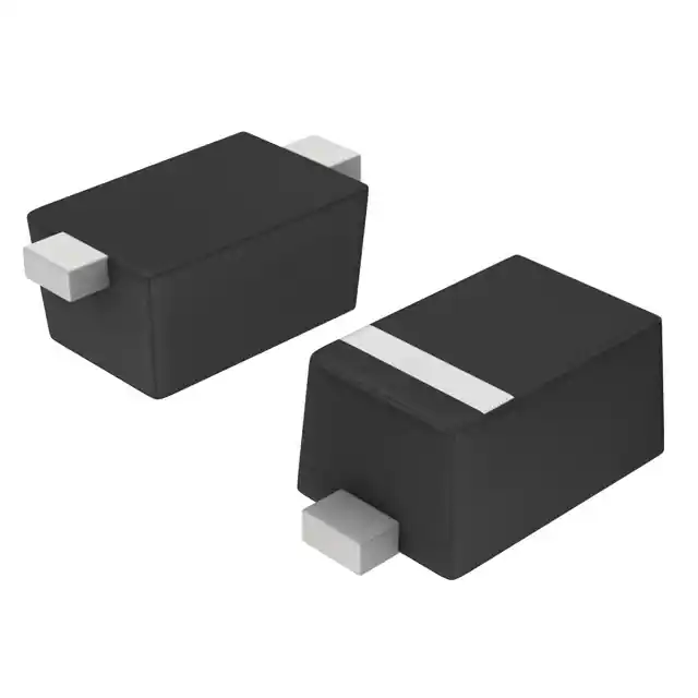
500 mW SOD−523 Surface Mount
This series of Zener diodes is packaged in a SOD−523 surface
mount package. They are designed to provide voltage regulation
protection and are especially attractive in situations where space is at a
premium. They are well suited for applications such as cellular
phones, hand held portables, and high density PC boards.
www.onsemi.com
SOD−523
CASE 502
STYLE 1
Specification Features
• Standard Zener Breakdown Voltage Range −2.4 V to 18 V
• Steady State Power Rating of 500 mW
• Small Body Outline Dimensions:
•
•
•
•
•
0.047″ x 0.032″ (1.20 mm x 0.80 mm)
Low Body Height: 0.028″ (0.7 mm)
ESD Rating of Class 3 (> 16 kV) per Human Body Model
Tight Tolerance VZ
SZ Prefix for Automotive and Other Applications Requiring Unique
Site and Control Change Requirements; AEC−Q101 Qualified and
PPAP Capable
These Devices are Pb−Free and are RoHS Compliant*
1
Cathode
2
Anode
MARKING DIAGRAM
1
XX MG
G
2
XX = Specific Device Code
M
Date Code*
G
= Pb−Free Package
(Note: Microdot may be in either location)
Mechanical Characteristics
CASE: Void-free, transfer-molded, thermosetting plastic
Epoxy Meets UL 94, V−0
LEAD FINISH: 100% Matte Sn (Tin)
MOUNTING POSITION: Any
*Date Code orientation may vary depending
upon manufacturing location.
QUALIFIED MAX REFLOW TEMPERATURE: 260°C
Device Meets MSL 1 Requirements
ORDERING INFORMATION
MAXIMUM RATINGS
Rating
Total Device Dissipation FR−4 Board,
(Note 1) @ TA = 25°C
Derate above 25°C
Thermal Resistance from
Junction−to−Ambient (Note 1)
Operating Junction and Storage
Temperature Range
Symbol
Max
Unit
500
4.0
mW
mW/°C
RqJA
250
°C/W
TJ, Tstg
−65 to
+150
°C
Device
Package
Shipping†
MM5ZxxxST1G
SOD−523
(Pb−Free)
3,000 /
Tape & Reel
SZMM5ZxxxST1G
SOD−523
(Pb−Free)
3,000 /
Tape & Reel
MM5ZxxxST5G
SOD−523
(Pb−Free)
8,000 /
Tape & Reel
SZMM5ZxxxST5G
SOD−523
(Pb−Free)
8,000 /
Tape & Reel
PD
Stresses exceeding those listed in the Maximum Ratings table may damage the
device. If any of these limits are exceeded, device functionality should not be
assumed, damage may occur and reliability may be affected.
1. FR−4 printed circuit board, single−sided copper, mounting pad 1 cm2.
†For information on tape and reel specifications,
including part orientation and tape sizes, please
refer to our Tape and Reel Packaging Specifications
Brochure, BRD8011/D.
DEVICE MARKING INFORMATION
*For additional information on our Pb−Free strategy and soldering details, please
download the ON Semiconductor Soldering and Mounting Techniques
Reference Manual, SOLDERRM/D.
© Semiconductor Components Industries, LLC, 2014
August, 2018 − Rev. 13
1
See specific marking information in the device marking
column of the Electrical Characteristics table on page 2 of
this data sheet.
Publication Order Number:
MM5Z2V4ST1/D
�MM5ZxxxST1G Series, SZMM5ZxxxST1G Series
ELECTRICAL CHARACTERISTICS
(TA = 25°C unless otherwise noted,
VF = 0.9 V Max. @ IF = 10 mA for all types)
Symbol
Parameter
VZ
Reverse Zener Voltage @ IZT
IZT
Reverse Current
ZZT
Maximum Zener Impedance @ IZT
IZK
Reverse Current
ZZK
Maximum Zener Impedance @ IZK
IR
Reverse Leakage Current @ VR
Reverse Voltage
IF
Forward Current
VF
Forward Voltage @ IF
C
VZ VR
V
IR VF
IZT
VR
QVZ
I
IF
Figure 1. Zener Voltage Regulator
Maximum Temperature Coefficient of VZ
Max. Capacitance @VR = 0 and f = 1 MHz
ELECTRICAL CHARACTERISTICS (VF = 0.9 Max @ IF = 10 mA for all types)
Zener Voltage
VZ
ZZT
IZ = IZT
@ 10%
Mod W
Max
mA
V
Min
Max
C pF Max @
VR = 0
f = 1 MHz
Max
IR @ VR
dVZ/dt (mV/k)
@ IZT1 = 5 mA
Min
Max
ZZK IZ
= 1.0
mA W
Max
5.0
2.43
2.63
1000
100
120
1.0
−3.5
0
450
T3
5.0
2.67
2.91
1000
100
100
1.0
−3.5
0
450
MM5Z3V3ST1G
T5
5.0
3.32
3.53
1000
95
5.0
1.0
−3.5
0
450
MM5Z3V6ST1G
T6
5.0
3.60
3.85
1000
90
5.0
1.0
−3.5
0
450
MM5Z3V9ST1G
T7
5.0
3.89
4.16
1000
90
3.0
1.0
−3.5
−2.5
450
MM5Z4V3ST1G
T8
5.0
4.17
4.43
1000
90
3.0
1.0
−3.5
0
450
MM5Z4V7ST1G/T5G
T9
5.0
4.55
4.75
800
80
3.0
2.0
−3.5
0.2
260
MM5Z5V1ST1G/T5G
TA
5.0
4.98
5.2
500
60
2.0
2.0
−2.7
1.2
225
MM5Z5V6ST1G/T5G
TC
5.0
5.49
5.73
200
40
1.0
2.0
−2.0
2.5
200
MM5Z6V2ST1G/T5G
TE
5.0
6.06
6.33
100
10
3.0
4.0
0.4
3.7
185
MM5Z6V8ST1G/T5G
TF
5.0
6.65
6.93
160
15
2.0
4.0
1.2
4.5
155
MM5Z7V5ST1G
TG
5.0
7.28
7.6
160
15
1.0
5.0
2.5
5.3
140
MM5Z8V2ST1G/T5G
TH
5.0
8.02
8.36
160
15
0.7
5.0
3.2
6.2
135
MM5Z9V1ST1G/T5G
TK
5.0
8.85
9.23
160
15
0.5
6.0
3.8
7.0
130
MM5Z12VST1G
TN
5.0
11.74
12.24
80
25
0.1
8.0
6.0
10
130
MM5Z16VST1G
TU
5.0
15.85
16.51
80
40
0.05
11.2
10.4
14
105
MM5Z18VST1G
TW
5.0
17.56
18.35
80
45
0.05
12.6
12.4
16
100
Device*
Device
Marking
Test
Current
Izt mA
MM5Z2V4ST1G/T5G
T2
MM5Z2V7ST1G
Product parametric performance is indicated in the Electrical Characteristics for the listed test conditions, unless otherwise noted. Product
performance may not be indicated by the Electrical Characteristics if operated under different conditions.
*Includes SZ-prefix devices where applicable.
www.onsemi.com
2
�MM5ZxxxST1G Series, SZMM5ZxxxST1G Series
TYPICAL CHARACTERISTICS
100
POWER DISSIPATION (%)
80
60
40
20
0
0
25
50
75
100
125
TEMPERATURE (°C)
Figure 2. Steady State Power Derating
www.onsemi.com
3
150
�MM5ZxxxST1G Series, SZMM5ZxxxST1G Series
PACKAGE DIMENSIONS
SOD−523
CASE 502
ISSUE E
−X−
D
NOTES:
1. DIMENSIONING AND TOLERANCING PER ASME Y14.5M, 1994.
2. CONTROLLING DIMENSION: MILLIMETERS.
3. MAXIMUM LEAD THICKNESS INCLUDES LEAD FINISH.
MINIMUM LEAD THICKNESS IS THE MINIMUM THICKNESS OF
BASE MATERIAL.
4. DIMENSIONS D AND E DO NOT INCLUDE MOLD FLASH, PROTRUSIONS, OR GATE BURRS.
−Y−
E
2X
b
0.08
1
M
2
X Y
DIM
A
b
c
D
E
HE
L
L2
TOP VIEW
A
c
MILLIMETERS
MIN
NOM
MAX
0.50
0.60
0.70
0.25
0.30
0.35
0.07
0.14
0.20
1.10
1.20
1.30
0.70
0.80
0.90
1.50
1.60
1.70
0.30 REF
0.15
0.20
0.25
STYLE 1:
PIN 1. CATHODE (POLARITY BAND)
2. ANODE
HE
SIDE VIEW
2X
RECOMMENDED
SOLDERING FOOTPRINT*
L
2X
1.80
0.48
2X
0.40
2X
L2
BOTTOM VIEW
PACKAGE
OUTLINE
DIMENSION: MILLIMETERS
*For additional information on our Pb−Free strategy and soldering
details, please download the ON Semiconductor Soldering and
Mounting Techniques Reference Manual, SOLDERRM/D.
ON Semiconductor and
are trademarks of Semiconductor Components Industries, LLC dba ON Semiconductor or its subsidiaries in the United States and/or other countries.
ON Semiconductor owns the rights to a number of patents, trademarks, copyrights, trade secrets, and other intellectual property. A listing of ON Semiconductor’s product/patent
coverage may be accessed at www.onsemi.com/site/pdf/Patent−Marking.pdf. ON Semiconductor reserves the right to make changes without further notice to any products herein.
ON Semiconductor makes no warranty, representation or guarantee regarding the suitability of its products for any particular purpose, nor does ON Semiconductor assume any liability
arising out of the application or use of any product or circuit, and specifically disclaims any and all liability, including without limitation special, consequential or incidental damages.
Buyer is responsible for its products and applications using ON Semiconductor products, including compliance with all laws, regulations and safety requirements or standards,
regardless of any support or applications information provided by ON Semiconductor. “Typical” parameters which may be provided in ON Semiconductor data sheets and/or
specifications can and do vary in different applications and actual performance may vary over time. All operating parameters, including “Typicals” must be validated for each customer
application by customer’s technical experts. ON Semiconductor does not convey any license under its patent rights nor the rights of others. ON Semiconductor products are not
designed, intended, or authorized for use as a critical component in life support systems or any FDA Class 3 medical devices or medical devices with a same or similar classification
in a foreign jurisdiction or any devices intended for implantation in the human body. Should Buyer purchase or use ON Semiconductor products for any such unintended or unauthorized
application, Buyer shall indemnify and hold ON Semiconductor and its officers, employees, subsidiaries, affiliates, and distributors harmless against all claims, costs, damages, and
expenses, and reasonable attorney fees arising out of, directly or indirectly, any claim of personal injury or death associated with such unintended or unauthorized use, even if such
claim alleges that ON Semiconductor was negligent regarding the design or manufacture of the part. ON Semiconductor is an Equal Opportunity/Affirmative Action Employer. This
literature is subject to all applicable copyright laws and is not for resale in any manner.
PUBLICATION ORDERING INFORMATION
LITERATURE FULFILLMENT:
Literature Distribution Center for ON Semiconductor
19521 E. 32nd Pkwy, Aurora, Colorado 80011 USA
Phone: 303−675−2175 or 800−344−3860 Toll Free USA/Canada
Fax: 303−675−2176 or 800−344−3867 Toll Free USA/Canada
Email: orderlit@onsemi.com
◊
N. American Technical Support: 800−282−9855 Toll Free
USA/Canada
Europe, Middle East and Africa Technical Support:
Phone: 421 33 790 2910
www.onsemi.com
4
ON Semiconductor Website: www.onsemi.com
Order Literature: http://www.onsemi.com/orderlit
For additional information, please contact your local
Sales Representative
MM5Z2V4ST1/D
�Mouser Electronics
Authorized Distributor
Click to View Pricing, Inventory, Delivery & Lifecycle Information:
ON Semiconductor:
SZMM5Z8V2ST1G SZMM5Z5V1ST1G SZMM5Z6V2ST1G SZMM5Z6V8ST1G SZMM5Z9V1ST5G
SZMM5Z5V1ST5G
�


 工商网监
湘ICP备2023018690号
工商网监
湘ICP备2023018690号
