TCP-3047H
4.7 pF Passive Tunable
Integrated Circuits (PTIC)
Introduction
ON Semiconductor’s PTICs have excellent RF performance and
power consumption, making them suitable for any mobile handset or
radio application. The fundamental building block of our PTIC
product line is a tunable material called ParaScant, based on Barium
Strontium Titanate (BST). PTICs have the ability to change their
capacitance from a supplied bias voltage generated by the Control IC.
The 4.7 pF PTICs are available as wafer-level chip scale packages
(WLCSP) and in QFN packages for easy mounting directly on printed
circuit boards.
www.onsemi.com
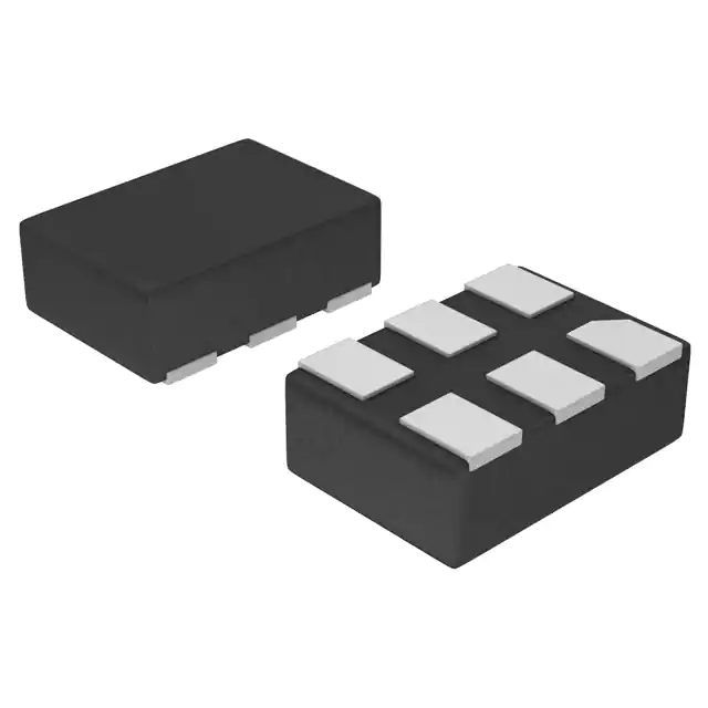
WLCSP12
1.18x0.72
CASE 567KE
QFN6
1.6x1.2
CASE 485DX
Key Features
•
•
•
•
•
•
•
•
•
High Tuning Range and Operation up to 20 V
Usable Frequency Range: from 700 MHz to 2.7 GHz
High Quality Factor (Q) for Low Loss
High Power Handling Capability
Compatible with PTIC Control IC TCC-103
WLCSP Package: 0.722 x 1.179 x 0.611 mm (12 pillar)
QFN Package: 1.200 x 1.600 x 0.950 mm
QFN: MSL−2 Moisture Sensitivity Level (per J−STD−020)
These devices are Pb−Free and RoHS Compliant
MARKING DIAGRAM
X.XH
X.X = 4.7
H = High Tuning
FUNCTIONAL BLOCK DIAGRAM
Typical Applications
•
•
•
•
PTIC
Multi-band, Multi-standard, Advanced and Simple Mobile Phones
Tunable Antenna Matching Networks
Tunable RF Filters
Active Antennas
RF1
RF2
Bias
PTIC Functional Block Diagram
ORDERING INFORMATION
Package
Shipping†
TCP−3047H−DT
WLCSP12
(Pb−Free)
4000 Units /
7” Reel
TCP−3047H−QT
QFN6
(Pb−Free)
8000 Units /
13“ Reel
Device
†For information on tape and reel specifications,
including part orientation and tape sizes, please
refer to our Tape and Reel Packaging Specifications
Brochure, BRD8011/D.
© Semiconductor Components Industries, LLC, 2016
May, 2016 − Rev. 3
1
Publication Order Number:
TCP−3047H/D
�TCP−3047H
DC Bias 1
A1
A2
NC
RF2
B1
B2
RF1
RF2
C1
C2
RF1
Figure 1. PTIC Functional Block Diagram (Top Level View)
Table 1. SIGNAL DESCRIPTIONS
Ball / Pad Number
Pin Name
A1
DC Bias 1
DC Bias Voltage
Description
B1
RF2
RF Input / Output
C1*
RF2
RF Input / Output
A2
NC
Not Connected
B2
RF1
RF Input / Output
C2*
RF1
RF Input / Output
*Ball/pad contains multiple connections. Please see packaging information on last page for more information.
www.onsemi.com
2
�TCP−3047H
TYPICAL SPECIFICATIONS
Representative Performance Data at 255C
Table 2. PERFORMANCE DATA
Parameter
Min
Typ
Units
20
V
Operating Bias Voltage
2.0
Capacitance (Vbias = 2 V)
4.23
4.70
5.17
pF
Capacitance (Vbias = 20 V)
1.18
1.24
1.30
pF
Tuning Range (2 V - 20 V)
3.40
3.80
4.20
Tuning Range (20 V - 2 V)
3.60
Leakage Current (WLCSP)
Operating Frequency
700
2.0
mA
2700
MHz
Quality Factor @ 700 MHz, 10 V
90
Quality Factor @ 2.4 GHz, 10 V
60
IP3 (Vbias = 2 V) [1,3]
70
dBm
85
dBm
-65
dBm
-80
dBm
-40
dBm
IP3 (Vbias = 20 V) [1,3]
2nd Harmonic (Vbias = 2 V)
[2,3]
2nd Harmonic (Vbias = 20 V)
3rd Harmonic (Vbias = 2 V)
[2,3]
[2,3]
3rd Harmonic (Vbias = 20 V)
1.
2.
3.
4.
Max
[2,3]
-70
dBm
Transition Time (Cmin ³ Cmax) [4]
80
ms
Transition Time (Cmax ³ Cmin) [4]
70
ms
f1 = 850 MHz, f2 = 860 MHz, Pin 25 dBm/Tone
850 MHz, Pin +34 dBm
IP3 and Harmonics are measured in the shunt configuration in a 50 W environment
RFIN and RFOUT are both connected to DC ground
www.onsemi.com
3
�TCP−3047H
Representative performance data at 255C for 4.7 pF WLCSP Package
Figure 2. Capacitance
Figure 3. Harmonic Power*
Figure 4. IP3*
Figure 5. Q*
*The data shown is based on the TCP−1047N device performance, for reference only. The TCP−3047H performance data will be available in
the Production Datasheet.
Table 3. ABSOLUTE MAXIMUM RATINGS
Parameter
Rating
Units
Input Power
+40
dBm
Bias Voltage
+25 (Note 5)
V
Operating Temperature Range
−30 to +85
°C
Storage Temperature Range
−55 to +125
°C
ESD − Human Body Model
Class 1A JEDEC HBM Standard (Note 6)
Stresses exceeding those listed in the Maximum Ratings table may damage the device. If any of these limits are exceeded, device functionality
should not be assumed, damage may occur and reliability may be affected.
5. WLCSP: Recommended Bias Voltage not to exceed 20 V
6. Class 1A defined as passing 250 V, but may fail after exposure to 500 V ESD pulse
www.onsemi.com
4
�TCP−3047H
ASSEMBLY CONSIDERATIONS AND REFLOW PROFILE
Molding
The following assembly considerations should be observed:
The PTIC die is compatible for over-molding or
under-fill.
Cleanliness
These chips should be handled in a clean environment.
Electro-static Sensitivity
ON Semiconductor’s PTICs are ESD Class 1A sensitive.
The proper ESD handling procedures should be used.
Mounting
The WLCSP PTIC is fabricated for Flip Chip solder
mounting. Connectivity to the RF and Bias terminations on
the PTIC die is established through copper pillar posts
(53 mm nominal height) topped with lead-free SAC351
solder caps (28 mm nominal height). The PTIC die is
RoHS-compliant and compatible with lead-free soldering
profile.
Post-reflow Cleaning
Use of ultrasonic cleaning is not recommended for
pillared devices as it may lead to premature fatigue failure
of the pillars.
Figure 6. Reflow Profile
ORIENTATION OF THE PTIC FOR OPTIMUM LOSSES
RF
When configuring the PTIC in your specific circuit
design, at least one of the RF terminals must be connected
to DC ground. If minimum transition times are required, DC
ground on both RF terminals is recommended. To minimize
losses, the PTIC should be oriented such that RF2 is at the
lower RF impedance of the two RF nodes. A shunt PTIC, for
example, should have RF2 connected to RF ground.
ANT
RF1
(PTIC Pad)
RF2
(PTIC Pad)
Bias
Figure 7. PTIC Orientation Functional Block
Diagram
www.onsemi.com
5
�TCP−3047H
PART NUMBER DEFINITION
Example: TCP−3047H−DT
TCP
-
30
47
H
-
D
T
Product
Family
Process Status
Process
Generation
Capacitor
Value
Tuning
Package /
Format
Packing
TCP
“blank” =
Production
X = Pilot
Production
10 = Gen 1.0
30 = Gen 3.0
12 = 1.2 pF
27 = 2.7 pF
33 = 3.3 pF
39 = 3.9 pF
47 = 4.7 pF
56 = 5.6 pF
68 = 6.8 pF
82 = 8.2 pF
N = Normal
H = High
D = WLCSP
Q = QFN
T = T&R
-
S=
Special/Custom
P = Prototype
-
Table 4. PART NUMBERS
Capacitance
2V
20 V
Package
TCP-3047H-DT
4.70
1.2
12-Pillar WLCSP
TCP-3047H-QT
4.70
1.2
6-Pin QFN
Part Number
www.onsemi.com
6
�TCP−3047H
PACKAGE DIMENSIONS
WLCSP12, 1.18x0.72
CASE 567KE
ISSUE O
È
È
PIN A1
REFERENCE
E
NOTES:
1. DIMENSIONING AND TOLERANCING PER
ASME Y14.5M, 1994.
2. CONTROLLING DIMENSION: MILLIMETERS.
3. COPLANARITY APPLIES TO SPHERICAL
CROWNS OF SOLDER BALLS.
A B
10X
b1
10X
D
b
0.05 C A B
DIM
A
A1
b
b1
D
E
e
e1
e2
e3
e4
0.03 C
DETAIL A
2X
0.05 C
2X
0.05 C
TOP VIEW
2X
b
2X
0.06 C
A
b1
0.05 C A B
0.03 C
RECOMMENDED
SOLDERING FOOTPRINT*
DETAIL B
0.05 C
A1
SIDE VIEW
NOTE 3
C
SEATING
PLANE
0.57
2X
e3
DETAIL A
0.15
A1
2X
e1
2X
0.13
0.52
PACKAGE
OUTLINE
e
F
E
D
C
B
MILLIMETERS
MIN
MAX
0.639
0.590
0.069
0.093
0.079
0.129
0.044
0.094
1.179 BSC
0.722 BSC
0.150 BSC
0.159 BSC
0.300 BSC
0.460 BSC
0.425 BSC
0.51
0.75
e2
2X
0.59
A
1
DIMENSIONS: MILLIMETERS
2
e4
0.13
*For additional information on our Pb−Free strategy and soldering
details, please download the ON Semiconductor Soldering and
Mounting Techniques Reference Manual, SOLDERRM/D.
DETAIL B
BOTTOM VIEW
www.onsemi.com
7
�TCP−3047H
PACKAGE DIMENSIONS
QFN6 1.6x1.2, 0.5P
CASE 485DX
ISSUE A
D
A
B
L
L
NOTES:
1. DIMENSIONING AND TOLERANCING PER
ASME Y14.5M, 1994.
2. CONTROLLING DIMENSION: MILLIMETERS.
L1
PIN ONE
IDENTIFIER
0.05 C
2X
2X
ÍÍÍ
ÍÍÍ
ÍÍÍ
0.05 C
DETAIL A
E
ALTERNATE TERMINAL
CONSTRUCTIONS
ÉÉ
ÉÉ
ÇÇ
EXPOSED Cu
TOP VIEW
A
DETAIL B
0.10 C
DIM
A
A1
A3
b
D
E
e
L
L1
MOLD CMPD
MILLIMETERS
MIN
MAX
0.90
1.00
0.00
0.05
0.15 REF
0.22
0.28
1.60 BSC
1.20 BSC
0.50 BSC
0.39
0.46
−−−
0.15
DETAIL B
ALTERNATE
CONSTRUCTIONS
A3
A1
0.05 C
C
SIDE VIEW
6X
RECOMMENDED
MOUNTING FOOTPRINT*
SEATING
PLANE
6X
b
0.60
0.10 C A
PACKAGE
OUTLINE
B
0.03 C
DETAIL A
1.40
1
1
6X
0.50
PITCH
L
6X
0.30
DIMENSIONS: MILLIMETERS
2
B
A
*For additional information on our Pb−Free strategy and soldering
details, please download the ON Semiconductor Soldering and
Mounting Techniques Reference Manual, SOLDERRM/D.
C
e
BOTTOM VIEW
ParaScan is a trademark of Paratek Microwave, Inc.
ON Semiconductor and
are registered trademarks of Semiconductor Components Industries, LLC (SCILLC). SCILLC owns the rights to a number of patents, trademarks,
copyrights, trade secrets, and other intellectual property. A listing of SCILLC’s product/patent coverage may be accessed at www.onsemi.com/site/pdf/Patent−Marking.pdf. SCILLC
reserves the right to make changes without further notice to any products herein. SCILLC makes no warranty, representation or guarantee regarding the suitability of its products for any
particular purpose, nor does SCILLC assume any liability arising out of the application or use of any product or circuit, and specifically disclaims any and all liability, including without
limitation special, consequential or incidental damages. “Typical” parameters which may be provided in SCILLC data sheets and/or specifications can and do vary in different applications
and actual performance may vary over time. All operating parameters, including “Typicals” must be validated for each customer application by customer’s technical experts. SCILLC
does not convey any license under its patent rights nor the rights of others. SCILLC products are not designed, intended, or authorized for use as components in systems intended for
surgical implant into the body, or other applications intended to support or sustain life, or for any other application in which the failure of the SCILLC product could create a situation where
personal injury or death may occur. Should Buyer purchase or use SCILLC products for any such unintended or unauthorized application, Buyer shall indemnify and hold SCILLC and
its officers, employees, subsidiaries, affiliates, and distributors harmless against all claims, costs, damages, and expenses, and reasonable attorney fees arising out of, directly or indirectly,
any claim of personal injury or death associated with such unintended or unauthorized use, even if such claim alleges that SCILLC was negligent regarding the design or manufacture
of the part. SCILLC is an Equal Opportunity/Affirmative Action Employer. This literature is subject to all applicable copyright laws and is not for resale in any manner.
PUBLICATION ORDERING INFORMATION
LITERATURE FULFILLMENT:
Literature Distribution Center for ON Semiconductor
P.O. Box 5163, Denver, Colorado 80217 USA
Phone: 303−675−2175 or 800−344−3860 Toll Free USA/Canada
Fax: 303−675−2176 or 800−344−3867 Toll Free USA/Canada
Email: orderlit@onsemi.com
N. American Technical Support: 800−282−9855 Toll Free
USA/Canada
Europe, Middle East and Africa Technical Support:
Phone: 421 33 790 2910
Japan Customer Focus Center
Phone: 81−3−5817−1050
www.onsemi.com
8
ON Semiconductor Website: www.onsemi.com
Order Literature: http://www.onsemi.com/orderlit
For additional information, please contact your local
Sales Representative
TCP−3047H/D
�