TN6726A / NZT6726
TN6726A
NZT6726
C
E
C
C
B
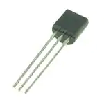
TO-226
B
SOT-223
E
PNP General Purpose Amplifier
This device is designed for general purpose medium power
amplifiers and switches requiring collector currents to 1.0 A.
Sourced from Process 77.
Absolute Maximum Ratings*
Symbol
TA = 25°C unless otherwise noted
Parameter
Value
Units
30
V
VCEO
Collector-Emitter Voltage
VCBO
Collector-Base Voltage
40
V
VEBO
Emitter-Base Voltage
5.0
V
IC
Collector Current - Continuous
TJ, Tstg
Operating and Storage Junction Temperature Range
1.5
A
-55 to +150
°C
*These ratings are limiting values above which the serviceability of any semiconductor device may be impaired.
NOTES:
1) These ratings are based on a maximum junction temperature of 150 degrees C.
2) These are steady state limits. The factory should be consulted on applications involving pulsed or low duty cycle operations.
3) All voltages (V) and currents (A) are negative polarity for PNP transistors.
Thermal Characteristics
Symbol
PD
TA = 25°C unless otherwise noted
Characteristic
RθJC
Total Device Dissipation
Derate above 25°C
Thermal Resistance, Junction to Case
RθJA
Thermal Resistance, Junction to Ambient
Max
*NZT6726
1.0
8.0
125
125
*Device mounted on FR-4 PCB 36 mm X 18 mm X 1.5 mm; mounting pad for the collector lead min. 6 cm2.
1997 Fairchild Semiconductor Corporation
Units
TN6726A
1.0
8.0
50
W
mW/°C
°C/W
°C/W
�(continued)
Electrical Characteristics
Symbol
TA = 25°C unless otherwise noted
Parameter
Test Conditions
Min
Max
Units
OFF CHARACTERISTICS
V(BR)CEO
IC = 10 mA, IB = 0
V(BR)CBO
Collector-Emitter Breakdown
Voltage
Collector-Base Breakdown Voltage
30
V
IC = 1.0 mA, IE = 0
40
V
V(BR)EBO
Emitter-Base Breakdown Voltage
5.0
V
ICBO
Collector-Cutoff Current
IE = 100 µA, IC = 0
VCB = 40 V, IE = 0
IEBO
Emitter-Cutoff Current
VEB = 5.0 V, IC = 0
0.1
µA
0.1
µA
TN6726A / NZT6726
PNP General Purpose Amplifier
ON CHARACTERISTICS*
hFE
DC Current Gain
VCE(sat)
Collector-Emitter Saturation Voltage
IC = 10 mA, VCE = 1.0 V
IC = 100 mA, VCE = 1.0 V
IC = 1.0 A, VCE = 1.0 V
IC = 1.0 A, IB = 100 mA
VBE(on)
Base-Emitter On Voltage
IC = 1.0 A, VCE = 1.0 V
55
60
50
250
0.5
V
1.2
V
SMALL SIGNAL CHARACTERISTICS
hfe
Small-Signal Current Gain
Ccb
Collector-Base Capacitance
IC = 50 mA, VCE = 10 V,
f = 20 MHz
VCB = 10 V, IE = 0, f = 1.0 MHz
2.5
25
30
pF
*Pulse Test: Pulse Width ≤ 300 µs, Duty Cycle ≤ 1.0%
3
NOTE: All voltages (V) and currents (A) are negative polarity for PNP transistors.
Typical Pulsed Current Gain
vs Collector Current
300
V CE = 5.0V
250
V CESAT- COLLE CTOR-EMITTER VOLTAGE (V)
h FE- TYP ICAL PULSED CURRE NT GAIN
Typical Characteristics
Collector-Emitter Saturation
Voltage vs Collector Current
1
β = 10
0.8
200
125 °C
0.6
150
25 °C
0.4
100
- 40 °C
0.2
50
0
0.01
0.1
1
I C - COLLECTOR CURRENT (A)
25 °C
2
0
0.01
- 40 °C
0.1
1
I C - COLLE CTOR CURRENT (A)
125 °C
3
�(continued)
Base-Emitter Saturation
Voltage vs Collector Current
β = 10
1
0.8
- 40 °C
25 °C
0.6
125 °C
0.4
1
IC
10
100
- COLLECTOR CURRENT ( mA)
1000
100
V CB = 2 0V
10
1
0.1
f T - GAIN BANDWIDTH PRODUCT (MHz)
25
50
75
100
125
T A - AM BIENT TE MPE RATURE (°C)
150
Base-Emitter ON Voltage vs
Collector Current
1
0.8
- 40 °C
125 °C
0.4
0.2
Gain Bandwidth Product
vs Collector Current
VCE = 5.0 V
1
200
150
100
50
Collector-Base Capacitance
vs Collector-Base Voltage
40
f = 1.0 MHz
30
20
10
0
0
IC
10
20
V CB- COLLECTOR-BASE VOLTAGE (V)
1000
DC
1
100
T
CO
L LE
DC
T
*PULSED
OPERATION
T A = 25 °C
0.1
30
10
µS
*
µS
*
CT
OR
LE
AM
AD
BIE
=2
5°
NT
=2
5°
1.0
ms
*
C
C
LIMIT DETERMINED
BY BV CEO
0.01
10
100
- COLLECTOR CURRENT (mA)
1000
10
V CE = 10V
1
10
100
I C - COLLECTOR CURRENT (mA)
Safe Operating Area TO-226 / SOT-223
250
0
25 °C
0.6
I C - COLLECTOR CURRENT (A)
I CBO - COLLECTOR CURRENT (nA)
Collector-Cutoff Current
vs Ambient Temperature
V BE(O N)- BASE-E MITTER ON VOLTAGE (V)
(continued)
COBO- COLLECTOR-BASE CAPACITANCE (pF)
V BESAT - BASE-EMITTER VOLTAG E (V)
Typical Characteristics
1
10
V CE - COLLECTOR-EMITTER VOLTAGE (V)
100
TN6726A / NZT6726
PNP General Purpose Amplifier
�(continued)
Typical Characteristics
(continued)
Power Dissipation vs
Ambient Temperature
PD - POWER DISSIPATION (W)
1
0.75
TN6726A / NZT6726
PNP General Purpose Amplifier
TO-226
SOT-223
0 .5
0.25
0
0
25
50
75
100
TEMPER ATURE (o C)
125
150
3
�TO-226AE Tape and Reel Data
TO -226AE Packaging
Conf iguratio n:
Fi gur e 1.0
TAPE and REEL OPTION
FSCINT Label sampl e
See Fig 2.0 for va rious
FAIRCHIL D S EMICONDUCTOR CORPORATION
L OT:
CBVK741B019
PN2222N
NSID:
D/C1:
QTY:
Reeling Styles
HTB:B
10000
SP EC:
FSCINT
D9842
SP EC RE V:
Labe l
B2
QA REV:
5 Reels per
Int er med iate B ox
(FSCINT)
Cus tom ized
F63TNR Label s ampl e
Labe l
LOT: CBVK7 41B019
FSID: PN222N
D/C1: D9842
D/C2:
F63TNR
QTY: 2000
Labe l
SPEC:
QTY1:
QTY2:
SPEC REV:
CPN:
N/F: F
Cus tom ized
Labe l
(F63TNR)3
375m m x 267m m x 375mm
Int er med iate B ox
AMMO PACK OPTION
See Fig 3.0 for 2 Ammo
Pack Options
TO-226AE TNR/AMMO PACKING INFO RMATION
Packing
Style
Quantity
Reel
A
2,000
D26Z
E
2,000
D27Z
Am m o
M
P
EOL code
2,000
Uni t wei gh t
FSCINT
D74Z
2,000
Labe l
D75Z
327m m x 158m m x 135mm
= 0.300g m
Reel weig ht wi th c om po nents
= 0.868 k g
Amm o weig ht wi th c omp on en ts
= 0.880 k g
Im med iate B ox
5 A mm o box es per
Int er med iate B ox
Cus tom ized
Labe l
Max q uanti ty p er i nte rm ed iate b ox = 10,000 un its
Cus tom ized
Labe l
F63TNR
Bar c ode Label
333m m x 231m m x 183mm
Int er med iate B ox
BULK OPTION
See Bulk Packing
Informat ion table
Anti -stati c
FSCINT Bar c ode Label
Bub ble Sheets
(TO-226AE ) BULK PACKING INFORMATION
EOL CODE
J18Z
J05Z
NO EOL
CODE
DESCRIPTION
LEADCLIP
DIMENSION
QUANTITY
TO-18 OPTION STD
NO L EAD CLIP
1.0 K / BOX
TO-5
NO L EAD CLIP
1.0 K / BOX
NO L EADCLIP
1.5 K / BOX
OPTION STD
TO-226 STANDARD
STRAIGHT
1,500 un its per
114m m x 102m m x 51mm
EO70 box for
s td o pti on
EO70 Im mediate B ox
5 EO70 boxes pe r
Int er med iate B ox
530m m x 130m m x 83mm
Inter med iate box
Cus tomized
Label
FSCINT Labe l
7,500 un its m axim um
per interm edi at e box
for st d opt ion
©2000 Fairchild Semiconductor International
October 1999, Rev. A1
�TO-226AE Tape and Reel Data, continued
TO-226AE Reeling Style
Configuration: Fi gure 2.0
Machine Option "A" (H)
Machine Option "E"(J)
Style "A" D26Z, D70Z (s/h)
Style "E" D 27Z, D71Z (s/h)
TO-226AE Radial Ammo Packaging
Configuration: Fi gure 3.0
FIRST WIRE OFF IS EMITTER (ON PKG. 92)
FIRST WIRE OFF IS COL LECTOR (ON PKG. 92)
ADHESIVE TAPE IS ON THE TOP SIDE
ADHESIVE TAPE IS ON THE TOP SIDE
FLAT OF TRANSISTOR IS ON BOTTOM
FLAT OF TRANSISTOR IS ON TOP
ORDER STYLE
D74Z (M)
ORDER STYLE
D75Z (P)
FIRST WIRE OFF IS EMITTER
FIRST WIRE OFF IS COL LECTOR
ADHESIVE TAPE IS ON BOTTOM SIDE
ADHESIVE TAPE IS ON BOTTOM SIDE
FLAT OF TRANSISTOR IS ON BOTTOM
FLAT OF TRANSISTOR IS ON TOP
October 1999, Rev. A1
�TO-226AE Tape and Reel Data, continued
TO-226AE Tape and Reel Taping
Dimension Configuration:
Fi gur e 4.0
Hd
P
Pd
b
Hb
W1
d
L
H1
HO
L1
S
WO
t
W2
W
t1
P1
F1
DO
P2
PO
User Direction of Feed
TO-226AE Reel
Configuration:
Fi gur e 5.0
ITEM DESCRI PTION
SYM BOL
DIMENSION
Base of Package to Lead Bend
b
0.098 (max)
Component Height
Hb
1.078 (+/- 0.050)
Lead Clinch He ight
HO
0.630 (+/- 0.020)
Component Base Heig ht
H1
0.748 (+/- 0.020)
Component Alignment (s ide / side )
Pd
0.040 (max)
Component Alignment ( front/back )
Hd
0.031 (max)
Component Pitch
P
0.500 (+/- 0.020)
Feed Hole Pitch
PO
0.500 (+/- 0.008)
Hole Center to First Lead
P1
0.150 (+0.009, -0.010 )
Hole Center to Component Center
P2
0.247 (+/- 0.007)
Lead Spread
F1/F2
0.104 (+/- 0 .010)
Lead Thickness
d
0.018 (+0.002, -0.003)
Cut Lead Length
L
0.429 (max)
Taped Lead Lengt h
L1
0.209 (+0.051, -0.052)
Taped Lead Thickness
t
0.032 (+/- 0.006)
Carrier Tape Thickness
t1
0.021 (+/- 0.006)
Carrier Tape Width
W
0.708 (+0.020, -0.019)
Hold - down Tape Width
WO
0.236 (+/- 0.012)
Hold - down Tape position
W1
0.035 (max)
Feed Hole Position
W2
0.360 (+/- 0.025)
Sprocket Hole Diameter
DO
0.157 (+0.008, -0.007)
Lead Spring O ut
S
0.004 (max)
Note : All dimensions are in inches.
E LE CT ROS TA TIC
S EN SI TIV E D EV ICE S
D4
D1
D2
F63TNR Label
ITEM DESCRIPT ION
SYMBOL
Reel Diamet er
D1
13.975
Arbor Hole Diameter (Standard)
D2
1.160
1.200
(Small Hole)
D2
0.650
0.700
Customized Label
MAXIMUM
14.025
Core Diameter
D3
3.100
3.300
Hub Recess Inner Diameter
D4
2.700
3.100
Hub Recess Dept h
W1
MINIMUM
W1
0.370
0.570
Flange to Flange Inner W idth
W2
1.630
1.690
Hu b to Hu b Cente r W idth
W3
2.09 0
W3
W2
Note: All dimensions are inches
D3
October 1999, Rev. A1
�TO-226AE Package Dimensions
TO-226AE (FS PKG Code 95, 99)
1:1
Scale 1:1 on letter size paper
Dimensions shown below are in:
inches [millimeters]
Part Weight per unit (gram): 0.300
S4.70-4.32;
S1.52-1.02;
2" TYP
S7.73-7.10;
S7.87-7.37;
2" TYP
S1.65-1.27;
0.51
S0.760.36;
S15.61-14.47;
S0.51-0.36;
S0.48-0.30;
S1.40-1.14;
PIN
S1.40-1.14;
99
95
1
E
E
2
B
C
3
C
B
S4.45-3.81;
5" TYP
1
2
3
TO-226AE (95,99)
S2.41-2.13;
©2000 Fairchild Semiconductor International
For leadformed option ordering,
refer to Tape & Reel data information.
October 1999, Rev. A1
�SOT-223 Tape and Reel Data
SOT-223 Packaging
Configuration: Figure 1.0
Customized Label
Packaging Description:
F63TNR Label
Antistatic Cover Tape
SOT-223 parts are shipped in tape. The carrier tape is
made from a dissipative (carbon filled) polycarbonate
resin. The cover tape is a multilayer film (Heat Activated
Adhesive in nature) primarily composed of polyester film,
adhesive layer, sealant, and anti-static sprayed agent.
These reeled parts in standard option are shipped with
2,500 units per 13" or 330cm diameter reel. The reels are
dark blue in color and is made of polystyrene plastic (antistatic coated). Other option comes in 500 units per 7" or
177cm diameter reel. This and some other options are
further described in the Packaging Information table.
These full reels are individually barcode labeled and
placed inside a standard intermediate box (illustrated in
figure 1.0) made of recyclable corrugated brown paper.
One box contains two reels maximum. And these boxes
are placed inside a barcode labeled shipping box which
comes in different sizes depending on the number of parts
shipped.
Static Dissipative
Embossed Carrier Tape
F852
014
F852
014
F852
014
F852
014
SOT-223 Packaging Information
Packaging Option
Packaging type
Qty per Reel/Tube/Bag
Reel Size
Box Dimension (mm)
Standard
(no flow code)
TNR
2,500
D84Z
SOT-223 Unit Orientation
TNR
500
13" Dia
7" Dia
343x64x343
184x187x47
Max qty per Box
5,000
1,000
Weight per unit (gm)
0.1246
0.1246
Weight per Reel (kg)
0.7250
0.1532
343mm x 342mm x 64mm
Intermediate box for Standard
F63TNR Label
Note/Comments
F63TNR Label
F63TNR Label sample
184mm x 184mm x 47mm
Pizza Box for D84Z Option
SOT-223 Tape Leader and Trailer
Configuration: Figure 2.0
LOT: CBVK741B019
QTY: 3000
FSID: PN2222A
SPEC:
D/C1: D9842
D/C2:
QTY1:
QTY2:
SPEC REV:
CPN:
N/F: F
(F63TNR)3
Carrier Tape
Cover Tape
Components
Trailer Tape
300mm minimum or
38 empty pockets
©2000 Fairchild Semiconductor International
Leader Tape
500mm minimum or
62 empty pockets
September 1999, Rev. B
�SOT-223 Tape and Reel Data, continued
SOT-223 Embossed Carrier Tape
Configuration: Figure 3.0
P0
D0
T
E1
F
K0
Wc
W
E2
B0
Tc
A0
D1
P1
User Direction of Feed
Dimensions are in millimeter
Pkg type
SOT-223
(12mm)
A0
6.83
+/-0.10
B0
7.42
+/-0.10
W
12.0
+/-0.3
D0
D1
1.55
+/-0.05
1.50
+/-0.10
E1
E2
1.75
+/-0.10
F
10.25
min
P1
5.50
+/-0.05
P0
8.0
+/-0.1
4.0
+/-0.1
K0
1.88
+/-0.10
Notes: A0, B0, and K0 dimensions are determined with respect to the EIA/Jedec RS-481
rotational and lateral movement requirements (see sketches A, B, and C).
T
Wc
0.292
+/0.0130
9.5
+/-0.025
0.06
+/-0.02
0.5mm
maximum
20 deg maximum
Typical
component
cavity
center line
B0
Tc
0.5mm
maximum
20 deg maximum component rotation
Typical
component
center line
Sketch A (Side or Front Sectional View)
A0
Component Rotation
Sketch C (Top View)
Component lateral movement
Sketch B (Top View)
SOT-223 Reel Configuration: Figure 4.0
Component Rotation
W1 Measured at Hub
Dim A
Max
Dim A
max
See detail AA
Dim N
7" Diameter Option
B Min
Dim C
See detail AA
W3
13" Diameter Option
Dim D
min
W2 max Measured at Hub
DETAIL AA
Dimensions are in inches and millimeters
Tape Size
Reel
Option
Dim A
Dim B
0.059
1.5
512 +0.020/-0.008
13 +0.5/-0.2
0.795
20.2
5.906
150
0.488 +0.078/-0.000
12.4 +2/0
0.724
18.4
0.469 – 0.606
11.9 – 15.4
0.059
1.5
512 +0.020/-0.008
13 +0.5/-0.2
0.795
20.2
7.00
178
0.488 +0.078/-0.000
12.4 +2/0
0.724
18.4
0.469 – 0.606
11.9 – 15.4
12mm
7" Dia
7.00
177.8
12mm
13" Dia
13.00
330
Dim C
Dim D
Dim N
Dim W1
Dim W2
Dim W3 (LSL-USL)
July 1999, Rev. B
�SOT-223 Package Dimensions
SOT-223 (FS PKG Code 47)
1:1
Scale 1:1 on letter size paper
Part Weight per unit (gram): 0.1246
©2000 Fairchild Semiconductor International
September 1999, Rev. C
�TRADEMARKS
The following are registered and unregistered trademarks Fairchild Semiconductor owns or is authorized to use and is
not intended to be an exhaustive list of all such trademarks.
ACEx™
Bottomless™
CoolFET™
CROSSVOLT™
DOME™
E2CMOSTM
EnSignaTM
FACT™
FACT Quiet Series™
FAST
FASTr™
GlobalOptoisolator™
GTO™
HiSeC™
ISOPLANAR™
MICROWIRE™
OPTOLOGIC™
OPTOPLANAR™
PACMAN™
POP™
PowerTrench
QFET™
QS™
QT Optoelectronics™
Quiet Series™
SILENT SWITCHER
SMART START™
SuperSOT™-3
SuperSOT™-6
SuperSOT™-8
SyncFET™
TinyLogic™
UHC™
VCX™
DISCLAIMER
FAIRCHILD SEMICONDUCTOR RESERVES THE RIGHT TO MAKE CHANGES WITHOUT FURTHER
NOTICE TO ANY PRODUCTS HEREIN TO IMPROVE RELIABILITY, FUNCTION OR DESIGN. FAIRCHILD
DOES NOT ASSUME ANY LIABILITY ARISING OUT OF THE APPLICATION OR USE OF ANY PRODUCT
OR CIRCUIT DESCRIBED HEREIN; NEITHER DOES IT CONVEY ANY LICENSE UNDER ITS PATENT
RIGHTS, NOR THE RIGHTS OF OTHERS.
LIFE SUPPORT POLICY
FAIRCHILD’S PRODUCTS ARE NOT AUTHORIZED FOR USE AS CRITICAL COMPONENTS IN LIFE SUPPORT
DEVICES OR SYSTEMS WITHOUT THE EXPRESS WRITTEN APPROVAL OF FAIRCHILD SEMICONDUCTOR CORPORATION.
As used herein:
1. Life support devices or systems are devices or
2. A critical component is any component of a life
support device or system whose failure to perform can
systems which, (a) are intended for surgical implant into
be reasonably expected to cause the failure of the life
the body, or (b) support or sustain life, or (c) whose
support device or system, or to affect its safety or
failure to perform when properly used in accordance
with instructions for use provided in the labeling, can be
effectiveness.
reasonably expected to result in significant injury to the
user.
PRODUCT STATUS DEFINITIONS
Definition of Terms
Datasheet Identification
Product Status
Definition
Advance Information
Formative or
In Design
This datasheet contains the design specifications for
product development. Specifications may change in
any manner without notice.
Preliminary
First Production
This datasheet contains preliminary data, and
supplementary data will be published at a later date.
Fairchild Semiconductor reserves the right to make
changes at any time without notice in order to improve
design.
No Identification Needed
Full Production
This datasheet contains final specifications. Fairchild
Semiconductor reserves the right to make changes at
any time without notice in order to improve design.
Obsolete
Not In Production
This datasheet contains specifications on a product
that has been discontinued by Fairchild semiconductor.
The datasheet is printed for reference information only.
Rev. G
�