NCV2393, TS393
Micropower Dual CMOS
Voltage Comparator
The NCV2393 and TS393 are micropower CMOS dual voltage
comparators. They feature extremely low consumption of 6 mA
typical per comparator and operate over a wide temperature range of
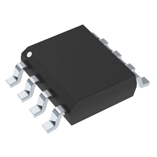
TA = −40 to 125°C. The NCV2393 and TS393 are available in an
SOIC−8 package.
www.onsemi.com
MARKING
DIAGRAM
Features
•
•
•
•
•
•
•
•
•
Extremely Low Supply Current: 6 mA Typical Per Channel
Wide Supply Range: 2.7 to 16 V
Extremely Low Input Bias Current: 1 pA Typical
Extremely Low Input Offset Current: 1 pA Typical
Input Common Mode Range Includes VSS
High Input Impedance: 1012 W
Pin−to−Pin Compatibility with Dual Bipolar LM393
NCV Prefix for Automotive and Other Applications Requiring
Unique Site and Control Change Requirements; AEC−Q100
Qualified and PPAP Capable
These Devices are Pb−Free, Halogen Free/BFR Free and are RoHS
Compliant
8
NCV2393
ALYW
G
SOIC−8
CASE 751
8
1
1
A
L
Y
W
G
= Assembly Location
= Wafer Lot
= Year
= Work Week
= Pb−Free Package
PIN CONNECTIONS
OUT 1
1
8
VDD
IN− 1
2
7
OUT 2
IN+ 1
3
6
IN− 2
VSS
4
5
IN+ 2
ORDERING INFORMATION
Package
Shipping†
NCV2393DR2G
SOIC−8
(Pb−Free)
2500 / Tape & Reel
TS393DR2G
SOIC−8
(Pb−Free)
2500 / Tape & Reel
Device
†For information on tape and reel specifications,
including part orientation and tape sizes, please
refer to our Tape and Reel Packaging Specifications
Brochure, BRD8011/D.
© Semiconductor Components Industries, LLC, 2014
June, 2017 − Rev. 5
1
Publication Order Number:
NCV2393/D
�NCV2393, TS393
PIN DESCRIPTION
Pin
Name
Type
1
OUT 1
Output
Description
2
IN− 1
Input
Inverting input of comparator 1
3
IN+ 1
Input
Non−inverting input of comparator 1
4
VSS
Power
5
IN+ 2
Input
Non−inverting input of comparator 2
Inverting input of comparator 2
Output of comparator 1. The open−drain output requires an external pull−up resistor.
Negative supply
6
IN− 2
Input
7
OUT 2
Output
Output of comparator 2. The open−drain output requires an external pull−up resistor.
8
VDD
Power
Positive supply
ABSOLUTE MAXIMUM RATINGS (Note 1)
Over operating free−air temperature, unless otherwise stated
Parameter
Limit
Unit
18
V
Input Voltage (Note 2)
18
V
Input Differential Voltage, VID (Note 3)
±18
V
Input Current (through ESD protection diodes)
50
mA
Output Voltage
18
V
Output Current
20
mA
Storage Temperature
−65 to +150
°C
Junction Temperature
150
°C
1500
V
50
V
100
mA
Supply Voltage, VS (VDD−VSS)
INPUT AND OUTPUT PINS
TEMPERATURE
ESD RATINGS
Human Body Model
Machine Model
LATCH−UP RATINGS
Latch−up Current
Stresses exceeding those listed in the Maximum Ratings table may damage the device. If any of these limits are exceeded, device functionality
should not be assumed, damage may occur and reliability may be affected.
1. Stresses beyond the absolute maximum ratings can lead to reduced reliability and damage.
2. Excursions of input voltages may exceed the power supply level. As long as the common mode voltage [VCM = (VIN+ + VIN−)/2] remains
within the specified range, the comparator will provide a stable output state. However, the maximum current through the ESD diodes of the
input stage must strictly be observed.
3. Input differential voltage is the non−inverting input terminal with respect to the inverting input terminal. To prevent damage to the gates, each
comparator includes back−to−back zener didoes between input terminals. When differential voltage exceeds 6.2 V, the diodes turn on. Input
resistors of 1 kW have been integrated to limit the current in this event.
4. This device series incorporates ESD protection and is tested by the following methods:
ESD Human Body Model tested per AEC−Q100−002 (JEDEC standard: JESD22−A114)
ESD Machine Model tested per AEC−Q100−003 (JEDEC standard: JESD22−A115)
Latch−up Current tested per JEDEC standard: JESD78.
THERMAL INFORMATION (Note 5)
Thermal Metric
Symbol
Value
Unit
Junction−to−Ambient (Note 6)
qJA
190
°C/W
Junction−to−Case Top
YJT
107
°C/W
5. Short−circuits can cause excessive heating and destructive dissipation. Values are typical.
6. Multilayer board, 1 oz. copper, 400 mm2 copper area, both junctions heated equally
www.onsemi.com
2
�NCV2393, TS393
OPERATING CONDITIONS
Symbol
Limit
Unit
Supply Voltage (VDD − VSS)
Parameter
VS
+2.7 to +16
V
Operating Free Air Temperature Range
TA
−40 to +125
°C
Functional operation above the stresses listed in the Recommended Operating Ranges is not implied. Extended exposure to stresses beyond
the Recommended Operating Ranges limits may affect device reliability.
ELECTRICAL CHARACTERISTICS: VS = +3 V
(Boldface limits apply over the specified temperature range, TA = –40°C to +125°C, guaranteed by characterization and/or design.)
Parameter
Symbol
Conditions
Min
VOS
VCM = mid−supply
Typ
Max
Unit
1.4
13
mV
14
mV
600
pA
INPUT CHARACTERISTICS
Offset Voltage
Input Bias Current (Note 7)
Input Offset Current (Note 7)
Input Common Mode Range
Common Mode Rejection
Ratio
IIB
IOS
VCM = mid−supply
1
VCM = mid−supply
pA
1
VCM
pA
300
pA
VSS
VDD –
1.5
V
VSS
VDD −
2
V
CMRR
VCM = VSS to VCM = VDD − 1.5 V
70
VOL
VID = −1 V, IOL = +6 mA
VSS +
300
dB
OUTPUT CHARACTERISTICS
Output Voltage Low
Output Current High
IOH
VID = +1 V, VOH = +3 V
2
VSS +
450
mV
VSS +
700
mV
40
nA
1000
nA
DYNAMIC PERFORMANCE
Propagation Delay Low to
High
tPLH
Propagation Delay High to
Low
tPHL
VCM = mid−supply,
f = 10 kHz, RPU = 5.1 kW,
CL = 50 pF
5 mV overdrive
2.1
ms
TTL input
0.6
ms
VCM = mid−supply,
f = 10 kHz, RPU = 5.1 kW,
CL = 50 pF
5 mV overdrive
3.9
ms
TTL input
0.2
ms
POWER SUPPLY
Power Supply Rejection Ratio
Quiescent Current
PSRR
VS = +3 V to +5 V
70
IDD
Per channel, no load, output = LOW
6
dB
15
mA
20
mA
Product parametric performance is indicated in the Electrical Characteristics for the listed test conditions, unless otherwise noted. Product
performance may not be indicated by the Electrical Characteristics if operated under different conditions.
7. Guaranteed by characterization and/or design.
www.onsemi.com
3
�NCV2393, TS393
ELECTRICAL CHARACTERISTICS: VS = +5 V, unless otherwise noted
(Boldface limits apply over the specified temperature range, TA = –40°C to +125°C, guaranteed by characterization and/or design.)
Parameter
Symbol
Conditions
Min
VOS
VCM = mid−supply V, VS = 5 V to 10 V
Typ
Max
Unit
1.4
13
mV
14
mV
INPUT CHARACTERISTICS
Offset Voltage
Input Bias Current
(Note 8)
IIB
VCM = mid−supply
1
Input Offset Current
(Note 8)
IOS
VCM = mid−supply
1
Input Common Mode
Range
VCM
Common Mode Rejection
Ratio
pA
600
pA
pA
300
pA
VSS
VDD –
1.5
V
VSS
VDD −
2
V
CMRR
VCM = VSS to VCM = VDD − 1.5 V
71
VOL
VID = −1 V, IOL = +6 mA
VSS +
260
dB
OUTPUT CHARACTERISTICS
Output Voltage Low
Output Current High
IOH
VID = +1 V, VOH = +5 V
2
VSS +
350
mV
VSS +
550
mV
40
nA
1000
nA
DYNAMIC PERFORMANCE
Fall Time
tFALL
Propagation Delay Low to
High
tPLH
Propagation Delay High
to Low
tPHL
25
ns
5 mV overdrive
2.1
ms
10 mV overdrive
1.2
ms
20 mV overdrive
0.8
ms
40 mV overdrive
0.5
ms
TTL input
0.6
ms
5 mV overdrive
5.8
ms
10 mV overdrive
3.2
ms
20 mV overdrive
1.7
ms
40 mV overdrive
1.0
ms
TTL input
0.3
ms
dB
50 mV overdrive, f = 10 kHz, RPU = 5.1 kW,
CL = 50 pF
VCM = mid−supply,
f = 10 kHz, RPU = 5.1 kW,
CL = 50 pF
VCM = mid−supply,
f = 10 kHz, RPU = 5.1 kW,
CL = 50 pF
POWER SUPPLY
Power Supply Rejection
Ratio
Quiescent Current
PSRR
VS = +5 V to = +10 V
80
IDD
Per channel, no load, output = LOW
6
15
mA
20
mA
Product parametric performance is indicated in the Electrical Characteristics for the listed test conditions, unless otherwise noted. Product
performance may not be indicated by the Electrical Characteristics if operated under different conditions.
8. Guaranteed by characterization and/or design
www.onsemi.com
4
�600
500
CURRENT (pA)
VS = 5 V
VCM = mid−rail
IIB+
IIB−
IOS
400
300
200
100
0
25
45
85
65
TEMPERATURE (°C)
105
125
VOL, LOW LEVEL OUTPUT VOLTAGE (V)
NCV2393, TS393
1.25
VS = 3 V
VS = 4 V
VS = 5 V
VS = 10 V
VS = 16 V
1
0.75
0.5
0.25
0
0
4
8
12
16
IOL, LOW−LEVEL OUTPUT CURRENT (mA)
450
400
Figure 2. VOL vs. IOL
25
VS = 5 V
IOL = 6 mA
IDD, SUPPLY CURRENT (mA)
VOL, LOW LEVEL OUTPUT VOLTAGE (mV)
Figure 1. IIB and IOS vs. Temperature
350
300
250
150
100
50
0
−55
−40
25
70
85
TA, FREE−AIR TEMPERATURE (°C)
20
15
5
0
125
Output Low
No Loads
Total IDD of both channels
0
2
4
6
8
10
12
VS, SUPPLY VOLTAGE (V)
Outputs High
PROPAGATION DELAY (nS)
IDD, SUPPLY CURRENT (mA)
900
12
10
Outputs Low
8
6
4
2
0
−55
VS = 5 V
No Loads
Total IDD of Both Channels
−40
25
70
85
14
16
Figure 4. IDD vs. VS
18
14
TA = −55°C
TA = −40°C
TA = 25°C
TA = 70°C
TA = 85°C
TA = 125°C
10
Figure 3. VOL vs. Temperature
16
20
800
700
600
tPLH
500
400
300
3
125
tPHL
Overdrive = 50 mV
RP = 5.1 kW
CL = 50 pF
TA = 25°C
6
9
12
15
18
21
24
27
30
VOH, HIGH LEVEL OUTPUT VOLTAGE (V)
VS, SUPPLY VOLTAGE (V)
Figure 5. IDD vs. Temperature
Figure 6. Propagation Delay vs. VS
www.onsemi.com
5
33
36
�NCV2393, TS393
5
VS = 5 V
0.35 RP = 5.1 kW
CL = 50 pF
0.3 T = 25°C
A
0.25
0.2
0.15
0.1
4
OUTPUT
3
2
40 mV
20 mV
1
2 mV
5 mV
0
−1
10 mV
−2
−3
0.05
−4
0
OUTPUT AMPLITUDE (V)
INPUT AMPLITUDE (V)
0.4
−5
−0.05 INPUT
0
−1
1
2
3
4
5
−6
PROPAGATION DELAY (ms)
Figure 7. tPLH vs. Overdrive
OUTPUT
0.3
0.25
20 mV
0.2
0.05
0
−1
−2
2 mV
0.1
70
1
10 mV
0.15
3
2
VS = 5 V
RP = 5.1 kW
CL = 50 pF
TA = 25°C
5 mV
40 mV
80
OUTPUT AMPLITUDE (V)
INPUT AMPLITUDE (V)
0.35
4
−3
INPUT
−4
0
−0.05
−3
−5
0
3
6
9
12
50 mV Overdrive
RP = 5.1k to VDD
TA = 25°C
60
50
CL = 50 pF
40
30
CL = 15 pF
20
10
0
−6
15
3
6
9
12
PROPAGATION DELAY (ms)
0.6
0.8
0.2
0
−0.2
−0.4
−0.6
−1
−1.5
VDD = 1.5 V
VSS = −1.5 V
−1.0
0.6
24
27 30
33 36
0
0.5
TA = −55°C
TA = −40°C
TA = 25°C
TA = 70°C
TA = 85°C
TA = 125°C
0.4
0.2
0
−0.2
−0.4
−0.6
−0.8
−0.5
21
1
TA = 70°C
TA = 85°C
TA = 125°C
0.4
−0.8
18
Figure 9. Fall Time vs. VS
OFFSET VOLTAGE (mV)
OFFSET VOLTAGE (mV)
0.8
TA = −55°C
TA = −40°C
TA = 25°C
15
VS, SUPPLY VOLTAGE (V)
Figure 8. tPHL vs. Overdrive
1
CL = 100 pF
tFall, FALL TIME (ns)
0.4
−1
−2.5
VDD = 2.5 V
VSS = −2.5 V
−2.0
−1.5
−1.0 −0.5
0
0.5
INPUT COMMON MODE VOLTAGE (V)
INPUT COMMON MODE VOLTAGE (V)
Figure 10. VOS vs. VCM (VS = 3 V)
Figure 11. VOS vs. VCM (VS = 5 V)
www.onsemi.com
6
1.0
1.5
�1
20
0.8
18
PERCENTAGE OF UNITS (%)
OFFSET VOLTAGE (mV)
NCV2393, TS393
0.6
0.4
0.2
0
−0.2
−0.4
−0.6
−0.8
−1
−1.5
VDD = 5 V
VSS = −5 V
TA = −55°C
TA = −40°C
TA = 25°C
−1.0
TA = 70°C
TA = 85°C
TA = 125°C
−0.5
0
16
14
12
10
8
6
4
2
0
0.5
n = 71545
TA = 25°C
VS = 3 V
VCM = mid−supply
−14 −12 −10 −8 −6 −4 −2 0
2
4
6
8 10 12 14
INPUT COMMON MODE VOLTAGE (V)
OFFSET VOLTAGE (mV)
Figure 12. VOS vs. VCM (VS = 10 V)
Figure 13. Offset Voltage Distribution
www.onsemi.com
7
�MECHANICAL CASE OUTLINE
PACKAGE DIMENSIONS
SOIC−8 NB
CASE 751−07
ISSUE AK
8
1
SCALE 1:1
−X−
DATE 16 FEB 2011
NOTES:
1. DIMENSIONING AND TOLERANCING PER
ANSI Y14.5M, 1982.
2. CONTROLLING DIMENSION: MILLIMETER.
3. DIMENSION A AND B DO NOT INCLUDE
MOLD PROTRUSION.
4. MAXIMUM MOLD PROTRUSION 0.15 (0.006)
PER SIDE.
5. DIMENSION D DOES NOT INCLUDE DAMBAR
PROTRUSION. ALLOWABLE DAMBAR
PROTRUSION SHALL BE 0.127 (0.005) TOTAL
IN EXCESS OF THE D DIMENSION AT
MAXIMUM MATERIAL CONDITION.
6. 751−01 THRU 751−06 ARE OBSOLETE. NEW
STANDARD IS 751−07.
A
8
5
S
B
0.25 (0.010)
M
Y
M
1
4
−Y−
K
G
C
N
X 45 _
SEATING
PLANE
−Z−
0.10 (0.004)
H
M
D
0.25 (0.010)
M
Z Y
S
X
J
S
8
8
1
1
IC
4.0
0.155
XXXXX
A
L
Y
W
G
IC
(Pb−Free)
= Specific Device Code
= Assembly Location
= Wafer Lot
= Year
= Work Week
= Pb−Free Package
XXXXXX
AYWW
1
1
Discrete
XXXXXX
AYWW
G
Discrete
(Pb−Free)
XXXXXX = Specific Device Code
A
= Assembly Location
Y
= Year
WW
= Work Week
G
= Pb−Free Package
*This information is generic. Please refer to
device data sheet for actual part marking.
Pb−Free indicator, “G” or microdot “G”, may
or may not be present. Some products may
not follow the Generic Marking.
1.270
0.050
SCALE 6:1
INCHES
MIN
MAX
0.189
0.197
0.150
0.157
0.053
0.069
0.013
0.020
0.050 BSC
0.004
0.010
0.007
0.010
0.016
0.050
0 _
8 _
0.010
0.020
0.228
0.244
8
8
XXXXX
ALYWX
G
XXXXX
ALYWX
1.52
0.060
0.6
0.024
MILLIMETERS
MIN
MAX
4.80
5.00
3.80
4.00
1.35
1.75
0.33
0.51
1.27 BSC
0.10
0.25
0.19
0.25
0.40
1.27
0_
8_
0.25
0.50
5.80
6.20
GENERIC
MARKING DIAGRAM*
SOLDERING FOOTPRINT*
7.0
0.275
DIM
A
B
C
D
G
H
J
K
M
N
S
mm Ǔ
ǒinches
*For additional information on our Pb−Free strategy and soldering
details, please download the ON Semiconductor Soldering and
Mounting Techniques Reference Manual, SOLDERRM/D.
STYLES ON PAGE 2
DOCUMENT NUMBER:
DESCRIPTION:
98ASB42564B
SOIC−8 NB
Electronic versions are uncontrolled except when accessed directly from the Document Repository.
Printed versions are uncontrolled except when stamped “CONTROLLED COPY” in red.
PAGE 1 OF 2
onsemi and
are trademarks of Semiconductor Components Industries, LLC dba onsemi or its subsidiaries in the United States and/or other countries. onsemi reserves
the right to make changes without further notice to any products herein. onsemi makes no warranty, representation or guarantee regarding the suitability of its products for any particular
purpose, nor does onsemi assume any liability arising out of the application or use of any product or circuit, and specifically disclaims any and all liability, including without limitation
special, consequential or incidental damages. onsemi does not convey any license under its patent rights nor the rights of others.
© Semiconductor Components Industries, LLC, 2019
www.onsemi.com
�SOIC−8 NB
CASE 751−07
ISSUE AK
DATE 16 FEB 2011
STYLE 1:
PIN 1. EMITTER
2. COLLECTOR
3. COLLECTOR
4. EMITTER
5. EMITTER
6. BASE
7. BASE
8. EMITTER
STYLE 2:
PIN 1. COLLECTOR, DIE, #1
2. COLLECTOR, #1
3. COLLECTOR, #2
4. COLLECTOR, #2
5. BASE, #2
6. EMITTER, #2
7. BASE, #1
8. EMITTER, #1
STYLE 3:
PIN 1. DRAIN, DIE #1
2. DRAIN, #1
3. DRAIN, #2
4. DRAIN, #2
5. GATE, #2
6. SOURCE, #2
7. GATE, #1
8. SOURCE, #1
STYLE 4:
PIN 1. ANODE
2. ANODE
3. ANODE
4. ANODE
5. ANODE
6. ANODE
7. ANODE
8. COMMON CATHODE
STYLE 5:
PIN 1. DRAIN
2. DRAIN
3. DRAIN
4. DRAIN
5. GATE
6. GATE
7. SOURCE
8. SOURCE
STYLE 6:
PIN 1. SOURCE
2. DRAIN
3. DRAIN
4. SOURCE
5. SOURCE
6. GATE
7. GATE
8. SOURCE
STYLE 7:
PIN 1. INPUT
2. EXTERNAL BYPASS
3. THIRD STAGE SOURCE
4. GROUND
5. DRAIN
6. GATE 3
7. SECOND STAGE Vd
8. FIRST STAGE Vd
STYLE 8:
PIN 1. COLLECTOR, DIE #1
2. BASE, #1
3. BASE, #2
4. COLLECTOR, #2
5. COLLECTOR, #2
6. EMITTER, #2
7. EMITTER, #1
8. COLLECTOR, #1
STYLE 9:
PIN 1. EMITTER, COMMON
2. COLLECTOR, DIE #1
3. COLLECTOR, DIE #2
4. EMITTER, COMMON
5. EMITTER, COMMON
6. BASE, DIE #2
7. BASE, DIE #1
8. EMITTER, COMMON
STYLE 10:
PIN 1. GROUND
2. BIAS 1
3. OUTPUT
4. GROUND
5. GROUND
6. BIAS 2
7. INPUT
8. GROUND
STYLE 11:
PIN 1. SOURCE 1
2. GATE 1
3. SOURCE 2
4. GATE 2
5. DRAIN 2
6. DRAIN 2
7. DRAIN 1
8. DRAIN 1
STYLE 12:
PIN 1. SOURCE
2. SOURCE
3. SOURCE
4. GATE
5. DRAIN
6. DRAIN
7. DRAIN
8. DRAIN
STYLE 13:
PIN 1. N.C.
2. SOURCE
3. SOURCE
4. GATE
5. DRAIN
6. DRAIN
7. DRAIN
8. DRAIN
STYLE 14:
PIN 1. N−SOURCE
2. N−GATE
3. P−SOURCE
4. P−GATE
5. P−DRAIN
6. P−DRAIN
7. N−DRAIN
8. N−DRAIN
STYLE 15:
PIN 1. ANODE 1
2. ANODE 1
3. ANODE 1
4. ANODE 1
5. CATHODE, COMMON
6. CATHODE, COMMON
7. CATHODE, COMMON
8. CATHODE, COMMON
STYLE 16:
PIN 1. EMITTER, DIE #1
2. BASE, DIE #1
3. EMITTER, DIE #2
4. BASE, DIE #2
5. COLLECTOR, DIE #2
6. COLLECTOR, DIE #2
7. COLLECTOR, DIE #1
8. COLLECTOR, DIE #1
STYLE 17:
PIN 1. VCC
2. V2OUT
3. V1OUT
4. TXE
5. RXE
6. VEE
7. GND
8. ACC
STYLE 18:
PIN 1. ANODE
2. ANODE
3. SOURCE
4. GATE
5. DRAIN
6. DRAIN
7. CATHODE
8. CATHODE
STYLE 19:
PIN 1. SOURCE 1
2. GATE 1
3. SOURCE 2
4. GATE 2
5. DRAIN 2
6. MIRROR 2
7. DRAIN 1
8. MIRROR 1
STYLE 20:
PIN 1. SOURCE (N)
2. GATE (N)
3. SOURCE (P)
4. GATE (P)
5. DRAIN
6. DRAIN
7. DRAIN
8. DRAIN
STYLE 21:
PIN 1. CATHODE 1
2. CATHODE 2
3. CATHODE 3
4. CATHODE 4
5. CATHODE 5
6. COMMON ANODE
7. COMMON ANODE
8. CATHODE 6
STYLE 22:
PIN 1. I/O LINE 1
2. COMMON CATHODE/VCC
3. COMMON CATHODE/VCC
4. I/O LINE 3
5. COMMON ANODE/GND
6. I/O LINE 4
7. I/O LINE 5
8. COMMON ANODE/GND
STYLE 23:
PIN 1. LINE 1 IN
2. COMMON ANODE/GND
3. COMMON ANODE/GND
4. LINE 2 IN
5. LINE 2 OUT
6. COMMON ANODE/GND
7. COMMON ANODE/GND
8. LINE 1 OUT
STYLE 24:
PIN 1. BASE
2. EMITTER
3. COLLECTOR/ANODE
4. COLLECTOR/ANODE
5. CATHODE
6. CATHODE
7. COLLECTOR/ANODE
8. COLLECTOR/ANODE
STYLE 25:
PIN 1. VIN
2. N/C
3. REXT
4. GND
5. IOUT
6. IOUT
7. IOUT
8. IOUT
STYLE 26:
PIN 1. GND
2. dv/dt
3. ENABLE
4. ILIMIT
5. SOURCE
6. SOURCE
7. SOURCE
8. VCC
STYLE 29:
PIN 1. BASE, DIE #1
2. EMITTER, #1
3. BASE, #2
4. EMITTER, #2
5. COLLECTOR, #2
6. COLLECTOR, #2
7. COLLECTOR, #1
8. COLLECTOR, #1
STYLE 30:
PIN 1. DRAIN 1
2. DRAIN 1
3. GATE 2
4. SOURCE 2
5. SOURCE 1/DRAIN 2
6. SOURCE 1/DRAIN 2
7. SOURCE 1/DRAIN 2
8. GATE 1
DOCUMENT NUMBER:
DESCRIPTION:
98ASB42564B
SOIC−8 NB
STYLE 27:
PIN 1. ILIMIT
2. OVLO
3. UVLO
4. INPUT+
5. SOURCE
6. SOURCE
7. SOURCE
8. DRAIN
STYLE 28:
PIN 1. SW_TO_GND
2. DASIC_OFF
3. DASIC_SW_DET
4. GND
5. V_MON
6. VBULK
7. VBULK
8. VIN
Electronic versions are uncontrolled except when accessed directly from the Document Repository.
Printed versions are uncontrolled except when stamped “CONTROLLED COPY” in red.
PAGE 2 OF 2
onsemi and
are trademarks of Semiconductor Components Industries, LLC dba onsemi or its subsidiaries in the United States and/or other countries. onsemi reserves
the right to make changes without further notice to any products herein. onsemi makes no warranty, representation or guarantee regarding the suitability of its products for any particular
purpose, nor does onsemi assume any liability arising out of the application or use of any product or circuit, and specifically disclaims any and all liability, including without limitation
special, consequential or incidental damages. onsemi does not convey any license under its patent rights nor the rights of others.
© Semiconductor Components Industries, LLC, 2019
www.onsemi.com
�onsemi,
, and other names, marks, and brands are registered and/or common law trademarks of Semiconductor Components Industries, LLC dba “onsemi” or its affiliates
and/or subsidiaries in the United States and/or other countries. onsemi owns the rights to a number of patents, trademarks, copyrights, trade secrets, and other intellectual property.
A listing of onsemi’s product/patent coverage may be accessed at www.onsemi.com/site/pdf/Patent−Marking.pdf. onsemi reserves the right to make changes at any time to any
products or information herein, without notice. The information herein is provided “as−is” and onsemi makes no warranty, representation or guarantee regarding the accuracy of the
information, product features, availability, functionality, or suitability of its products for any particular purpose, nor does onsemi assume any liability arising out of the application or use
of any product or circuit, and specifically disclaims any and all liability, including without limitation special, consequential or incidental damages. Buyer is responsible for its products
and applications using onsemi products, including compliance with all laws, regulations and safety requirements or standards, regardless of any support or applications information
provided by onsemi. “Typical” parameters which may be provided in onsemi data sheets and/or specifications can and do vary in different applications and actual performance may
vary over time. All operating parameters, including “Typicals” must be validated for each customer application by customer’s technical experts. onsemi does not convey any license
under any of its intellectual property rights nor the rights of others. onsemi products are not designed, intended, or authorized for use as a critical component in life support systems
or any FDA Class 3 medical devices or medical devices with a same or similar classification in a foreign jurisdiction or any devices intended for implantation in the human body. Should
Buyer purchase or use onsemi products for any such unintended or unauthorized application, Buyer shall indemnify and hold onsemi and its officers, employees, subsidiaries, affiliates,
and distributors harmless against all claims, costs, damages, and expenses, and reasonable attorney fees arising out of, directly or indirectly, any claim of personal injury or death
associated with such unintended or unauthorized use, even if such claim alleges that onsemi was negligent regarding the design or manufacture of the part. onsemi is an Equal
Opportunity/Affirmative Action Employer. This literature is subject to all applicable copyright laws and is not for resale in any manner.
PUBLICATION ORDERING INFORMATION
LITERATURE FULFILLMENT:
Email Requests to: orderlit@onsemi.com
onsemi Website: www.onsemi.com
◊
TECHNICAL SUPPORT
North American Technical Support:
Voice Mail: 1 800−282−9855 Toll Free USA/Canada
Phone: 011 421 33 790 2910
Europe, Middle East and Africa Technical Support:
Phone: 00421 33 790 2910
For additional information, please contact your local Sales Representative
�