Revised October 2004
USB1T1102
Universal Serial Bus Peripheral Transceiver
with Voltage Regulator
General Description
Features
This chip provides a USB Transceiver functionality with a
voltage regulator that is compliant to USB Specification
Rev 2.0. this integrated 5V to 3.3V regulator allows interfacing of USB Application specific devices with supply voltages ranging from 1.65V to 3.6V with the physical layer of
Universal Serial Bus. It is capable of operating at 12Mbits/s
(full speed) data rates and hence is fully compliant to USB
Specification Rev 2.0. The Vbusmon pin allows for monitoring the Vbus line.
■ Complies with Universal Serial Bus Specification 2.0
The USB1T1102 also provides exceptional ESD protection
with 15kV contact HBM on D+, D− pins.
■ 15kV contact HBM ESD protection on bus pins
■ Integrated 5V to 3.3V voltage regulator for powering
VBus
■ Utilizes digital inputs and outputs to transmit and receive
USB cable data
■ Supports full speed (12Mbits/s) data rates
■ Ideal for portable electronic devices
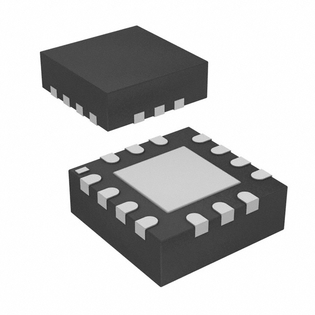
■ MLP technology package (16 pin) with HBCC footprint
Ordering Code:
Order Number
Package Number
Package Description
USB1T1102MPX
MLP14D
14-Terminal Molded Leadless Package (MLP), 2.5mm Square
USB1T1102RMPX
(Preliminary)
MLP14D
14-Terminal Molded Leadless Package (MLP), 2.5mm Square
USB1T1102MHX
MLP16HB
16-Terminal Molded Leadless Package (MHBCC), JEDEC MO-217, 3mm Square
USB1T1102RMHX
(Preliminary)
MLP16HB
16-Terminal Molded Leadless Package (MHBCC), JEDEC MO-217, 3mm Square
Logic Diagram
Note: On the USB1T1102R (Preliminary) the 1.5k resistor is integrated into the part,
and connects VPU and D+ eliminating the need for this external pull-up resistor.
© 2004 Fairchild Semiconductor Corporation
DS500877
www.fairchildsemi.com
USB1T1102 Universal Serial Bus Peripheral Transceiver with Voltage Regulator
August 2004
�USB1T1102
Connection Diagrams
MLP16 GND Exposed Diepad
MLP14 GND Exposed Diepad
(Bottom View)
(Bottom View)
Terminal Descriptions
Terminal Number
MLP14
MLP16
Terminal
Name
I/O
1
1
OE
I
Output Enable:
Active LOW enables the transceiver to transmit data on the bus. When not
active the transceiver is in the receive mode (CMOS level is relative to VCCIO)
2
2
RCV
O
Receive Data Output:
Non-inverted CMOS level output for USB differential Input (CMOS output level
is relative to VCCIO). Driven LOW when SUSPN is HIGH; RCV output is stable
and preserved during SE0 condition.
3
3
Vp/Vpo
I/O
Single-ended D+ receiver output VP (CMOS level relative to VCCIO):
Used for external detection of SE0, error conditions, speed of connected device;
Pin also acts as drive data input Vpo (see Table 1 and Table 2).
Output drive is 4 mA buffer.
4
4
Vm/Vmo
I/O
Single-ended D− receiver output Vm (CMOS level relative to VCCIO):
Used for external detection of SE0, error conditions, speed of connected device;
Pin also acts as drive data input Vmo (see Table 1 and Table 2).
Output drive is 4 mA buffer.
5
5
SUSPND
I
—
6
NC
6
7
VCCIO
7
8
Vbusmon
O
9, 8
10, 9
D+ , D −
AI/O
Terminal Description
Suspend:
Enables a low power state (CMOS level is relative to VCCIO). While the
SUSPND pin is active (HIGH) it will drive the RCV pin to logic “0” state.
No Connect
Supply Voltage for digital I/O pins (1.65V to 3.6V):
When not connected the D+ and D− pins are in 3-STATE. This supply bus is
totally independent of VCC (5V) and VREG (3.3V).
Vbus monitor output (CMOS level relative to VCCIO):
When Vbus > 4.1V then Vbusmon = HIGH and when Vbus < 3.6V then
Vbusmon = LOW. If SUSPND = HIGH then Vbusmon is pulled HIGH.
Data +, Data −:
Differential data bus conforming to the USB standard.
10
11
NC
No Connect
—
12
NC
No Connect
11
13
VREG (3.3V)
Internal Regulator Option:
Regulated supply output voltage (3.0V to 3.6V) during 5V operation;
decoupling capacitor of at least 0.1 µF is required.
Regulator ByPass Option:
Used as supply voltage input for 3.3V operation.
12
14
VCC (5.0V)
Internal Regulator Option:
Used as supply voltage input (4.0V to 5.5V); can be connected directly to USB
line Vbus.
Regulator ByPass Option:
Connected to VREG (3.3V)
www.fairchildsemi.com
2
�Terminal Number
(Continued)
MLP14
MLP16
Terminal
Name
13
15
VPU (3.3V)
14
16
Config
I
GND
GND
Exposed Exposed
Diepad Diepad
I/O
Terminal Description
Pull-up Supply Voltage (3.3V ± 10%):
Connect an external 1.5kΩ resistor on D+ (FS data rate);
Pin function is controlled by Config input pin:
Config = LOW − VPU (3.3V) is floating (High Impedance) for zero pull-up current.
Config = HIGH − VPU (3.3V) = 3.3V; internally connected to VREG (3.3V).
USB connect or disconnect software control input.
Configures 3.3V to external 1.5kΩ resistor on D+ when HIGH.
GND supply down bonded to exposed diepad to be connected to the PCB GND.
Functional Description
The USB1T1102 differs from earlier USB Transceiver in
that the Vp/Vm and Vpo/Vmo pins are now I/O pins rather
than discrete input and output pins. Table 1 describes the
specific pin functionality selection. Table 2 and Table 3
describe the specific Truth Tables for Driver and Receiver
operating functions.
The USB1T1102 transceiver is designed to convert CMOS
data into USB differential bus signal levels and to convert
USB differential bus signal to CMOS data.
To minimize EMI and noise the outputs are edge rate controlled with the rise and fall times controlled and defined for
full speed data rates only (12Mbits/s). The rise, fall times
are balanced between the differential pins to minimize
skew.
The USB1T1102 also has the capability of various power
supply configurations to support mixed voltage supply
applications (see Table 4) and Section 2.1 for detailed
descriptions.
Functional Tables
TABLE 1. Function Select
SUSPND
OE
D+, D−
RCV
Vp/Vpo
Vm/Vmo
L
L
Driving &
Receiving
Active
Vpo Input
Vmo Input
L
H
Receiving
(Note 1)
Active
Vp Output
Vm Output Receiving
H
L
Driving
Inactive
(Note 2)
Vpo Input
Vmo Input
H
H
3-STATE
(Note 1)
Inactive
(Note 2)
Vp Output
Vm Output Low Power State
Function
Normal Driving
(Differential Receiver Active)
Driving during Suspend
(Differential Receiver Inactive)
Note 1: Signal levels is function of connection and/or pull-up/pull-down resistors.
Note 2: For SUSPND = HIGH mode the differential receiver is inactive and the output RCV is forced LOW. The out-of-suspend signaling (K) is detected via
the single-ended receivers of the Vp/Vpo and Vm/Vmo pins.
TABLE 2. Driver Function (OE = L) using Differential Input Interface
Vm/Vmo
Vp/Vpo
Data
L
L
SE0 (Note 3)
L
H
Differential Logic 1
H
L
Differential Logic 0
H
H
Illegal State
Note 3: SE0 = Single Ended Zero
TABLE 3. Receiver Function (OE = H)
D+ , D−
RCV
Vp/Vpo
Differential Logic 1
H
H
L
Differential Logic 0
L
L
H
SE0
X
L
L
Vm/Vmo
X = Don’t Care
3
www.fairchildsemi.com
USB1T1102
Terminal Descriptions
�USB1T1102
Power Supply Configurations and Options
• Sharing Mode: VCCIO is only supply connected. VCC and
VREG are not connected. In this mode the D+ and D−
pins are 3-STATE and the USB1T1102 allows external
signals up to 3.6V to share the D+ and D− bus lines.
Internally the circuitry limits leakage from D+ and D−
pins (maximum 10 µA) and VCCIO such that device is in
low power (suspended) state. Pins Vbusmon and RCV
are forced LOW as an indication of this mode with Vbusmon being ignored during this state.
The two modes of power supply operation are:
• Normal Mode: VCCIO and VCC (5V) are connected or
VCCIO, VCC (5V) and [VREG (3.3V) and VCC (5V) shorted
for Bypass mode]
1. For 5V operation VCC is connected to 5V source
(4.0V to 5.5V) and the internal voltage regulator then
produces 3.3V for the USB connections.
2. For 3.3V operation both VCC and VREG are connected to a 3.3V source (3.0V to 3.6V)
A summary of the Supply Configurations is described in
Table 4.
In both cases for normal mode the VCCIO is an independent voltage source (1.65V to 3.6V) that is a function of
the external circuit configuration.
TABLE 4. Power Supply Configuration Options
Pins
Power Supply Mode Configuration
Sharing
Normal (Regulated Output)
Normal (Regulator Bypass)
VCC (5V)
Not Connected
Connected to 5V Source
Connected to VREG (3.3V)
[Max Drop of 0.3V]
(2.7V to 3.6V)
VREG (3.3V)
Not Connected
3.3V, 300 µA
Regulated Output
Connected to 3.3V Source
VCCIO
1.65V to 3.6V Source
1.65V to 3.6V Source
1.65V to 3.6V Source
VPU (3.3V)
3-STATE (Off)
3.3V Available if
Config = HIGH
3.3V Available if
Config = HIGH
D +, D−
3-STATE
Function of Mode Set Up
Function of Mode Set Up
Vp/Vpo, Vm/Vmo
L
Function of Mode Set Up
Function of Mode Set Up
RCV
L
Function of Mode Set Up
Function of Mode Set Up
Vbusmon
L
Function of Mode Set Up
Function of Mode Set Up
OE, SUSPND, Config
Hi-Z
Function of Mode Set Up
Function of Mode Set Up
www.fairchildsemi.com
4
�USB1T1102
ESD Protection
ESD Performance of the USB1T1102
HBM D+/D−: 15.0kV
HBM, all other pins (Mil-Std 883E): 6.5kV
ESD Protection: D+/D− Pins
Since the differential pins of a USB transceiver may be
subjected to extreme ESD voltages, additional immunity
has been included in the D+ and D− pins without compromising performance. The USB1T1102 differential pins have
ESD protection to the following limits:
FIGURE 1. Human Body ESD Test Model
• 15kV using the contact Human Body Model
• 8kV using the Contact Discharge method as specified in
IEC 61000-4-2
Human Body Model
Figure 1 shows the schematic representation of the Human
Body Model ESD event. Figure 2 is the ideal waveform representation of the Human Body Model.
IEC 61000-4-2, IEC 60749-26 and IEC 60749-27
The IEC 61000-4-2 standard covers ESD testing and performance of finished equipment, and as such evaluates the
equipment in its entirety for ESD immunity. Fairchild
Semiconductor has evaluated this device using the
IEC 6100-4-2 representative system model depicted in Figure 3. Under the additional standards set forth by the IEC,
this device is also compliant with IEC 60749-26 (HBM) and
IEC 60749-27 (MM).
FIGURE 2. HBM Current Waveform
Additional ESD Test Conditions
For additional information regarding our product test methodologies and performance levels, please contact Fairchild
Semiconductor.
FIGURE 3. IEC 61000-4-2 ESD Test Model
5
www.fairchildsemi.com
�USB1T1102
Absolute Maximum Ratings(Note 4)
Supply Voltage (VCC)(5V)
−0.5V to +6.0V
I/O Supply Voltage (VCCIO)
−0.5V to +4.6V
Recommended Operating
Conditions
DC Supply Voltage VCC (5V)
Latch-up Current (ILU)
4.0V to 5.5V
I/O DC Voltage VCCIO
VI = −1.8V to +5.4V
150 mA
0V to VCCIO +5.5V
DC Input Voltage Range (VI)
DC Input Current (IIK)
VI < 0
1.65V to 3.6V
DC Input Range for AI/O (VAI/O)
−50 mA
0V to VCC
Pins D+ and D−
DC Input Voltage (VI)
0V to 3.6V
Operating Ambient Temperature
−0.5V to VCCIO +5.5V
(Note 5)
−40°C to +85°C
(TAMB)
DC Output Diode Current (IOK)
VO > VCC or VO < 0
±50 mA
DC Output Voltage (VO)
−0.5V to VCCIO + 0.5V
(Note 5)
Output Source or Sink Current (IO)
VO = 0 to VCC
Current for D+, D− Pins
±50 mA
Current for RCV, Vm/Vp
±15 mA
DC VCC or GND Current
±100 mA
(ICC, IGND)
ESD Immunity Voltage (VESD);
Contact HBM
Pins D+, D−, VCC (5.5V) and GND
Note 4: The Absolute Maximum Ratings are those values beyond which
the safety of the device cannot be guaranteed. The device should not be
operated at these limits. The parametric values defined in the Electrical
Characteristic tables are not guaranteed at the absolute maximum rating.
The “Recommended Operating Conditions” table will define the conditions
for actual device operation.
15kV
All Other Pins
6.5kV
Storage Temperature (TSTO)
−40°C to + 125°C
Power Dissipation (PTOT)
ICC (5V)
Note 5: IO Absolute Maximum Rating must be observed.
48 mW
ICCIO
9 mW
DC Electrical Characteristics (Supply Pins)
Over recommended range of supply voltage and operating free air temperature (unless otherwise noted).
VCC (5V) = 4.0V to 5.5V or VREG (3.3V) = 3.0V to 3.6V, VCCIO = 1.65V to 3.6V
Limits
Symbol
VREG (3.3V)
Parameter
Regulated Supply Output
−40°C to +85°C
Conditions
Internal Regulator Option;
ILOAD ≤ 300 µA
Units
Min
Typ
Max
3.0
3.3
3.6
4.0
8.0
(Note 6)(Note 7)
ICC
Operating Supply Current (VCC5.0)
Transmitting and Receiving at
ICCIO
I/O Operating Supply Current
Transmitting and Receiving at
ICC (IDLE)
Supply Current during
IDLE: VD+ ≥ 2.7V, VD− ≤ 0.3V;
12 Mbits/s; CLOAD = 50 pF (D+, D−)
12 Mbits/s
(Note 8)
1.0
2.0
(Note 8)
300
FS IDLE and SE0 (VCC5.0)
SE0: VD+ ≤ 0.3V, VD− ≤ 0.3V
ICCIO (STATIC)
I/O Static Supply Current
IDLE, SUSPND or SE0
20.0
ICC(SUSPND)
Suspend Supply Current
SUSPND = HIGH
25.0
USB1T1102
OE = HIGH
(Note 9)
SUSPND = HIGH
USB1T1102R
OE = HIGH
mA
mA
µA
µA
(Note 9)
Vm = Vp = OPEN
Suspend Supply Current
V
40.0
µA
(Note 10)
Vp = Vm = OPEN
ICCIO(SHARING) I/O Sharing Mode Supply Current
VCC (5V) Not Connected
ID+ (SHARING)
Sharing Mode Load Current on
VCC (5V) Not Connected
D+/D− Pins
Config = LOW; VD± = 3.6V
www.fairchildsemi.com
6
20.0
µA
10.0
µA
�(Continued)
Limits
Symbol
Parameter
−40°C to +85°C
Conditions
Min
VCCTH
VCC Threshold Detection Voltage
Units
Typ
Max
1.65V ≤ VCCIO ≤ 3.6V
Supply Lost
3.6
Supply Present
VCCHYS
VCC Threshold Detection
VCCIO = 1.8V
70.0
Hysteresis Voltage
VCCIOTH
VCCIO Threshold Detection Voltage
mV
2.7V ≤ VREG ≤ 3.6V
Supply Lost
0.5
Supply Present
VCCIOHYS
VCCIO Threshold Detection
Regulated Supply Threshold
Detection Voltage
VREG = 3.3V
450
2.7V ≤ VREG ≤ 3.6V
V
0.8
Supply Present
Regulated Supply Threshold
mV
1.65V ≤ VCCIO ≤ VREG
Supply Lost
VREGHYS
V
1.4
Hysteresis Voltage
VREGTH
V
4.1
2.4 (Note 11)
VCCIO = 1.8V
450
Detection Hysteresis Voltage
mV
Note 6: ILOAD includes the pull-up resistor current via pin VPU
Note 7: The minimum voltage in Suspend mode is 2.7V.
Note 8: Not tested in production, value based on characterization.
Note 9: Excludes any current from load and VPU current to the 1.5kΩ resistor.
Note 10: Includes current between Vpu and the 1.5k internal pull-up resistor.
Note 11: When VCCIO < 2.7V, minimum value for VREGTH = 2.0V for supply present condition.
DC Electrical Characteristics
(Digital Pins – excludes D+, D− Pins)
Over recommended range of supply voltage and operating free air temperature (unless otherwise noted). VCCIO = 1.6V to 3.6V
Limits
Symbol
Parameter
Test Conditions
−40°C to +85°C
Min
Units
Max
Input Levels
VIL
LOW Level Input Voltage
VIH
HIGH Level Input Voltage
0.3
0.6*V CCIO
V
V
OUTPUT LEVELS:
VOL
VOH
LOW Level Output Voltage
HIGH Level Output Voltage
IOL = 2 mA
0.4
IOL = 100 µA
0.15
IOH = 2 mA
VCCIO - 0.4
IOH = 100 µA
VCCIO- 0.15
V
V
Leakage Current
ILI
Input Leakage Current
VCCIO = 1.65V to 3.6V
Input Capacitance
Pin to GND
±1.0
(Note 12)
µA
10.0
pF
Capacitance
CIN, CI/O
Note 12: If VCCIO ≥ VREG then leakage current will be higher than specified.
7
www.fairchildsemi.com
USB1T1102
DC Electrical Characteristics
�USB1T1102
DC Electrical Characteristics (Analog I/O Pins – D+, D− Pins)
Over recommended range of supply voltage and operating free air temperature (unless otherwise noted).
VCC = 4.0V to 5.5V or VREG = 3.0V to 3.6V
Limits
Symbol
Parameter
−40°C to +85°C
Test Condition
Min
Typ
Units
Max
Input Levels – Differential Receiver
VDI
Differential Input Sensitivity
VCM
Differential Common Mode Voltage
| VI(D+) - VI(D−) |
0.2
V
0.8
2.5
V
0.8
V
INPUT LEVELS – Single-ended Receiver
VIL
LOW Level Input Voltage
VIH
HIGH Level Input Voltage
2.0
VHYS
Hysteresis Voltage
0.30
V
0.7
V
0.3
V
3.6
V
±1.0
µA
20.0
pF
Output Levels
VOL
LOW Level Output Voltage
RL = 1.5kΩ to 3.6V
VOH
HIGH Level Output Voltage
RL = 15kΩ to GND
2.8
(Note 13)
Leakage Current
IOFF
Input Leakage Current Off State
CAPACITANCE
CI/O
I/O Capacitance
Pin to GND
Resistance
ZDRV
Driver Output Impedance
ZIN
Driver Input Impedance
RSW
Switch Resistance
VTERM
Termination Voltage
41.0
(Note 14)
MΩ
10.0
RPU Upstream Port
Note 13: If VOH min. = VREG - 0.2V.
Note 14: Includes external resistors of 29Ω on both D+ and D− pins.
Note 15: This voltage is available at pin VPU and V REG.
Note 16: Minimum voltage is 2.7V in the suspend mode.
www.fairchildsemi.com
Ω
10.0
8
3.0
(Note 15)
(Note 16)
Ω
3.6
V
�Over recommended range of supply voltage and operating free air temperature (unless otherwise noted).
VCC = 4.0V to 5.5V or VREG = 3.0V to 3.6V, VCCIO = 1.65V to 3.6V, CL = 50 pF; RL = 1.5K on D+ to VPU
Limits
Symbol
Parameter
−40°C to +85°C
Test Conditions
Min
Typ
Unit
Max
Driver Characteristics
tR
Output Rise Time
CL = 50 − 125 pF
4.0
20.0
4.0
20.0
90.0
111.1
%
1.3
2.0
V
Figures 5, 8
18.0
ns
Figures 7, 9
15.0
ns
Figures 7, 9
15.0
ns
Figures 6, 10
15.0
ns
Figures 6, 10
18.0
ns
10% to 90%
ns
tF
Output Fall Time
Figures 4, 8
tRFM
Rise/Fall Time Match
tF/ tR Excludes First Transition
VCRS
Output Signal Crossover Voltage
from Idle State
(Note 17)
Excludes First Transition from
Idle State see Waveform
Driver Timing
tPLH
Propagation Delay
tPHL
(Vp/Vpo, Vm/Vmo to D+/D−)
tPHZ
Driver Disable Delay
tPLZ
(OE to D+/D−)
tPZH
Driver Enable Delay
tPZL
(OE to D+/D−)
Receiver Timing
tPLH
Propagation Delay (Diff)
tPHL
(D+/D− to Rev)
tPLH
Single Ended Receiver Propagation Delay
tPHL
(D+/D− to Vp/ Vpo, V m/Vmo)
Note 17: Not production tested, guaranteed by characterization.
9
www.fairchildsemi.com
USB1T1102
AC Electrical Characteristics (A I/O Pins Full Speed)
�USB1T1102
Typical Application Configurations
Upstream Connection in Bypass Mode with Differential Outputs
Downstream Connection in Normal Mode with Differential Outputs
www.fairchildsemi.com
10
�USB1T1102
AC Waveforms
FIGURE 4. Rise and Fall Times
FIGURE 5. Vpo, Vmo to D+/D−
FIGURE 6. D+/D− to RCV, Vpo/Vp and Vmo/Vm
FIGURE 7. OE to D+/D−
Test Circuits and Waveforms
CL = 50 pF Full Speed Propagation Delays
CL = −125 pF Edge Rates only
V = 0 for tPZH, tPHZ
V = VREG for tPZL
FIGURE 8. Load for D+/D−
FIGURE 9. Load for Enable and Disable Times
FIGURE 10. Load for Vm/Vmo, Vp/Vpo and RCV
11
www.fairchildsemi.com
�USB1T1102
Tape and Reel Specification
Tape Format for MLP
Package
Designator
MP/MH
Tape
Number
Cavity
Section
Cavities
Status
Cover Tape
Status
Leader (Start End)
125 (typ)
Empty
Sealed
Carrier
2500/3000
Filled
Sealed
Trailer (Hub End)
75 (typ)
Empty
Sealed
TAPE DIMENSIONS inches (millimeters)
REEL DIMENSIONS inches (millimeters)
Tape Size
12 mm
A
B
C
D
N
W1
W2
13.0
0.059
0.512
0.795
7.008
0.488
0.724
330
(1.50)
(13.00)
(20.20)
(178)
(12.4)
(18.4)
www.fairchildsemi.com
12
�USB1T1102
Physical Dimensions inches (millimeters) unless otherwise noted
14-Terminal Molded Leadless Package (MLP), 2.5mm Square
MLP14D
13
www.fairchildsemi.com
�USB1T1102 Universal Serial Bus Peripheral Transceiver with Voltage Regulator
Physical Dimensions inches (millimeters) unless otherwise noted (Continued)
16-Terminal Molded Leadless Package (MHBCC), JEDEC MO-217, 3mm Square
Package Number MLP16HB
Fairchild does not assume any responsibility for use of any circuitry described, no circuit patent licenses are implied and
Fairchild reserves the right at any time without notice to change said circuitry and specifications.
LIFE SUPPORT POLICY
FAIRCHILD’S PRODUCTS ARE NOT AUTHORIZED FOR USE AS CRITICAL COMPONENTS IN LIFE SUPPORT
DEVICES OR SYSTEMS WITHOUT THE EXPRESS WRITTEN APPROVAL OF THE PRESIDENT OF FAIRCHILD
SEMICONDUCTOR CORPORATION. As used herein:
2. A critical component in any component of a life support
device or system whose failure to perform can be reasonably expected to cause the failure of the life support
device or system, or to affect its safety or effectiveness.
1. Life support devices or systems are devices or systems
which, (a) are intended for surgical implant into the
body, or (b) support or sustain life, and (c) whose failure
to perform when properly used in accordance with
instructions for use provided in the labeling, can be reasonably expected to result in a significant injury to the
user.
www.fairchildsemi.com
www.fairchildsemi.com
14
�This datasheet has been download from:
www.datasheetcatalog.com
Datasheets for electronics components.
�


 工商网监
湘ICP备2023018690号
工商网监
湘ICP备2023018690号
