XOCLCC6EVB
Crystal Clock Oscillator
Module Evaluation Board
User's Manual for NBX
Family in 6 Pin CLCC 5 mm
x 7 mm Package
http://onsemi.com
EVAL BOARD USER’S MANUAL
Generic Evaluation Board: XOCLCC6EVB
Devices: NBXxxxx
Description
Evaluation Board Manual Document Features
This Evaluation Board user’s manual is a guide for using
the XOCLCC6EVB Evaluation Board to provide a
convenient platform for quickly evaluating, characterizing
and verify performance and operation of a device in the
NBXxxxx family of Clock Oscillator Modules packaged in
the 6 pin CLCC, 5mm by 7 mm, CASE 848AB (see
Appendix).
This family of devices offer an internal crystal and PLL
IC. This Evaluation Board Manual and Evaluation Board
should be used in conjunction with a specific device data
sheet, which contains full technical details on specifications
and operation.
An NBXxxxx Clock Oscillator Module device may be
directly solder mounted onto the available evaluation board
footprint; or multiple units may be inserted and tested by
solder mounting a separate insertion socket (P/N
AM0393−320R from SER Electronics) onto the available
footprint.
•
•
•
•
•
•
•
Information on the XOCLCC6EVB Evaluation Board
Appropriate Lab Setup and Procedures
Board build Bill of Materials (Table 5)
Evaluation Board schematic (Figure 7)
Evaluation Board Lamination Stackup (Figure 8)
Evaluation Board Fabrication Notes
Appendix:
− Mechanical Case Outline
− Generic Marking Diagram
− Soldering Footprint
What measurements can you expect to make?
With this evaluation board, the following measurements
could be performed in single−ended or differential modes of
operation.
• DC Characteristics
• Frequency Performance
• Output Rise and Fall Time
• Phase Noise
• Jitter
Evaluation Board Features
• 6 pin CLCC solder footprint for solder mounting a
device or test socket
• Incorporates jumper headers to conveniently and
manually control the levels for the ’Output Enable’
(Pin 1) and ’Frequency Select’ (Pin 2) pins.
• Enable single or split−power supply operation.
LVPECL differential outputs are accessed via SMA
connectors offering different output load configurations.
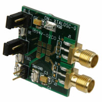
Front
Back
Figure 1. Evaluation Board Images (Front and Back)
© Semiconductor Components Industries, LLC, 2012
February, 2012 − Rev. 2
1
Publication Order Number:
EVBUM2076/D
�XOCLCC6EVB
EVALUATION BOARD MAP
3
2
H
1
L
VDD
4
5
J1
OE
H
L
11
10
J2
FSEL
6
SMAGND
C3
7
C4
DUTGND
8
9
Figure 2. Evaluation Board Layout
Table 1. EVALUATION BOARD MAP DESCRIPTION
Number
Description
1
DUT PIN6 Positive supply connection anvil and test point.
2
Decoupling capacitors. See BOM/board schematic for details.
3
DUT PIN 4 OE jumper header to force logic HIGH (Active) or LOW (Outputs Disabled to High Impedance).
Leave open or use jumper to force HIGH (OE Pin defaults HIGH when left floating) (see Figure 3 below)
4
OE connection anvil and test point.
5
DUT PIN 2 FSEL jumper header to force logic HIGH or LOW. FSEL Pin defaults HIGH when left floating. (see
Figure 3 below)
6
FSEL connection anvil and test point.
7
Device ground (DUTGND) connection anvil and test point.
8
DUT PIN 3 GND/SMAGND jumper header to force DUTGND connection to SMAGND. (see Figure 3 below)
9
SMAGND connection anvil and test point.
10
SMA outputs (CLK/CLK).
11
6 pin CLCC 5mmX7mm DUT (Device under test).
http://onsemi.com
2
�XOCLCC6EVB
Evaluation Board Jumper Headers on OE (Pin 4), FSEL (Pin 5)
Evaluation Board Jumper Header on DUTGND (Pin 3)
Figure 3. Select Positions for Evaluation Board Jumper Headers on OE (Pin 4), FSEL (Pin 5), and DUTGND (Pin 3)
TIME DOMAIN MEASUREMENTS
Equipment
Table 3. XOCLCC6EVB POWER SUPPLY
CONNECTION VOLTAGES
Table 2 indicates the recommended equipment for
making characterization and performance measurements.
Table 2. BASIC EQUIPMENT
Description
Example Equipment
Qty
Power Supply with 4
outputs
HP6624A or similar
1
Real−Time Oscilloscope
DPO70804 or similar
1
Matched High Speed
Cables with SMA
Connectors
Storm, Semflex, or
similar
2
Power supply cables
4
A). Single
Positive
+3.3 V Setup
B). Split 3.3 V
Setup
C). Single
Negative
−3.3 V Setup
VDD = 3.3 V
VDD = 2.0 V
VDD = 0 V
VTT
= VDD − 2.0 V
= 1.3 V
VTT
= VDD − 2.0 V
= SMAGND
=0V
VTT
= VDD − 2.0 V
= −2.0 V SMAGND
= VDD = 0 V
DUTGND
= SMAGND
=0V
DUTGND
= −1.3 V
DUTGND = −3.3 V
NOTE: SMAGND is the SMA cable shield reference for
the inputs and outputs only, not to be confused
with the device ground pin (DUTGND).
Setup
The following steps should be followed for proper
equipment setup.
Step 2: Connect Output Signals
Table 4 gives a list of specific LOGIC Levels and their
appropriate Power Supply and Typical Lab Setup
conditions
LVPECL: The LVPECL outputs have standard, open
emitter outputs and must be externally DC loaded and AC
terminated. A split power supply technique takes advantage
of terminating the LVPECL outputs into 50 W of an
oscilloscope or a frequency counter. Since VTT = VDD – 2 V,
offsetting VDD to +2.0 V yields VTT = 0 V or Ground
(SMAGND). The VTT terminal connects to the isolated
SMAGND connector ground plane, and is not to be
confused with the device ground pin (DUTGND). (See
Application Note AN8020/D for details on ECL
termination).
CML: For CML lab setup and test, operation with
negative supply voltage is recommended to enable the 50 W
internal impedance in the oscilloscope to be used as a
termination of the CML signals (VDD = 0.0 V, SMAGND =
0.0 V, and DUTGND = −3.3 V (See Application Note
AN8173/D for details on CML termination).
Step 1: Connect Power (split power supply mode)
Three power levels must be provided to the board: VDD,
DUTGND, and SMAGND via the test point anvils at the
edges of the board. Bypass capacitors are installed from
VDD to SMAGND and DUTGND to SMAGND near the test
points (see BOM). Devices may be tested in one of three
supply modes (see Table 3):
A). Single (Positive) +3.3 V Setup
No offset to supplies or output levels
B). Split 3.3 V Setup
Offsets the VDD, DUTGND, and output voltage levels by
−1.3 V and avoids an additional, separate VTT supply and
allows a direct connection to test equipment such as an
oscilloscope or counter with 50 W impedance to GND
inputs. SMAGND = VTT = VDD – 2.0 V = 0.0 V.
C). Single (Negative) −3.3 V Setup
Offsets the VDD, DUTGND, and output voltage levels by
−3.3 V
http://onsemi.com
3
�XOCLCC6EVB
Step 3: Configure FSEL and OE
LVDS: Driver termination is a 100 W resistor across the
differential lines located at the receiver input.
The FSEL and OE control pins can be controlled from an
external source via the appropriate test point, or via the
jumper headers located on the evaluation board, as indicated
in Figures 2 and 7. Refer to the specific device datasheet for
details on the proper settings for these pins.
Table 4. TYPICAL LAB SETUP
LOGIC Levels
Power Supply
Typical Lab Setup
LVPECL
Split 3.3 V
See Figure 4
CML
Single −3.3 V
See Figure 5
LVDS
Single 3.3 V
See Figure 6
+2.0V
Digital Oscilloscope
Or Frequency Counter
VDD = +2.0V
H
L
VDD
+
+2.0V
OE
−
H
J1
L
50W
Power Supply
J2
FSEL
+
+1.3V
SMAGND
−
50W
C3
C4
DUTGND
VEE = −1.3
−1.3
0V
Figure 4. Split Power Supply Lab Setup for LVPECL Outputs (DO NOT JUMPER DUTGND and SMAGND)
http://onsemi.com
4
�XOCLCC6EVB
0V
0V
VDD = SMAGND = 0V
Digital Oscilloscope
Or Frequency Counter
H
L
VDD
+
0V
OE
−
H
J1
L
50W
Power Supply
+
FSEL
−3.3V
J2
SMAGND
−
C4
DUTGND
VEE = −3.3V
50W
C3
0V
−3.3V
Note: For CML outputs, 50 W to VDD is needed for proper termination. See application note AND8173/D.
Figure 5. Typical Lab Setup for CML Outputs (DO NOT JUMPER DUTGND and SMAGND)
+3.3V
H L
VDD
Power Supply
OE
Digital Oscilloscope
J1
H L
+
100W
+3.3V
High Impedance
Differential
Probe
−
FSEL
J2
SMAGND
C3
Jumper
C4
DUTGND
0V
Figure 6. Typical Lab Setup for LVDS Outputs (JUMPER DUTGND and SMAGND)
http://onsemi.com
5
�XOCLCC6EVB
Table 5. XOCLCC6EVB EVALUATION BOARD BILL OF MATERIALS
Components
Manufacturer
Description
Part Number
Qty
Jumper Header
Berg
100 mil
In House
5
Test Point
Keystone
Anvil SMD
5016
3
Connector
Johanson
SMA, Edge Mount
142−0711−821
2
Capacitor
Kemet
22 mF, 10%
T491D22K016AS, Case C or D
2
Capacitor
Kemet
0.1 mF, 10%
C0603C104K4RAC
2
Socket (Not Supplied)
SER Electronics
Socket − 6−Lead 5mm x 7mm
AM0393−320R
1
Shunt
VDD
VDD
Jumper Header
Test
Point
Test
Point
VDD
OE
VDD
FSEL
CLK
GND
(DUTGND)
CLK
DUTGND
Test
Point
J1
SMA
Jumper Header
J2
DUTGND
SMA
Test
Point
VDD
DUTGND
Jumper Header
DUTGND
SMAGND
22mF
0.1mF
SMAGND
22mF
0.1mF
SMAGND
Figure 7. XOCLCC6EVB Evaluation Board Schematic
Figure 8. XOCLCC6EVB Evaluation Board Layer Lamination Stackup
http://onsemi.com
6
�XOCLCC6EVB
Evaluation Board Fabrication Notes
10. Warp and twist of single sided boards shall not
exceed 0.002”per inch, warp and twist of
multi−layer boards shall not exceed 0.010” per
inch.
11. All dimensions are in inches unless otherwise
specified tolerances. XX "0.010” XXX "0.004”.
12. Acceptability requirements per IPC−A−600E.
13. Drawing is viewed from component or primary
side.
14. This is a 4 layer board.
15. All holes are plated thru unless otherwise
specified.
16. Drill size units are thousandths of an inch.
17. Trim all silkscreen which flows over via holes or
SMD pads.
18. Break all sharp edges, PCB edges should be
smooth and even.
1. Material: FR−4
2. Finished copper to be loz. (0.0014) external layers
3. Minimum copper plating 0.0007” thick for plated
thru holes annular ring to be 0.0002” minimum
4. LPI soldermask green
5. Soldermask registration "0.002” N/A
6. All exposed copper areas to be gold plated
(0.000030” gold over 0.000100” nickel)
7. If specified, silkscreen is to be white epoxy ink.
8. Hole diameter tolerance is "0.002”, maximum
layer to layer misregistration shall be 0.004”,
measurement method must comply with
MIL−P−55110D, Figure 1.
9. Finished conductor width shall not vary more than
"0.001” from artwork master 50 W traces are
0.024” wide.
http://onsemi.com
7
�XOCLCC6EVB
Appendix:
Mechanical Case Outline
Generic Marking Diagram
Soldering Footprint
PACKAGE DIMENSIONS
6 PIN CLCC, 7x5, 2.54P
CASE 848AB−01
ISSUE C
A
D
4X
0.15 C
E2
TERMINAL 1
INDICATOR
NOTES:
1. DIMENSIONING AND TOLERANCING PER
ASME Y14.5M, 1994.
2. CONTROLLING DIMENSION: MILLIMETERS.
B
D1
H E1
DIM
A
A1
A2
A3
b
D
D1
D2
D3
E
E1
E2
E3
e
H
L
R
E
D2
TOP VIEW
A2
A3
0.10 C
A
SIDE VIEW
A1
C
SEATING
PLANE
D3
3
2
1
R
6X
b
6
5
4
6X
4.37
4.65
1.17
GENERIC
MARKING DIAGRAM*
XXXXX
A
WL
YY
WW
G
L
SOLDERING FOOTPRINT*
= Specific Device Code
= Assembly Location
= Wafer Lot
= Year
= Work Week
= Pb−Free Package
*This information is generic. Please refer
to device data sheet for actual part marking.
Pb−Free indicator, “G” or microdot “ G”,
may or may not be present.
6X
2.54
PITCH
6.17
6.66
1
BOTTOM VIEW
1.50
0.08
1.30
MILLIMETERS
NOM
MAX
1.80
1.90
0.70 REF
0.36 REF
0.10
0.12
1.40
1.50
7.00 BSC
6.20
6.23
6.81
6.96
5.08 BSC
5.00 BSC
4.40
4.43
4.80
4.95
3.49 BSC
2.54 BSC
1.80 REF
1.27
1.37
0.70 REF
XXXXXXXXX
XXXXXXXXXXXXX
AWLYYWWG
E3
0.10 C A B
0.05 C
e
MIN
1.70
5.06
6X
1.50
DIMENSION: MILLIMETERS
*For additional information on our Pb−Free strategy and soldering
details, please download the ON Semiconductor Soldering and
Mounting Techniques Reference Manual, SOLDERRM/D.
http://onsemi.com
8
�onsemi,
, and other names, marks, and brands are registered and/or common law trademarks of Semiconductor Components Industries, LLC dba “onsemi” or its affiliates
and/or subsidiaries in the United States and/or other countries. onsemi owns the rights to a number of patents, trademarks, copyrights, trade secrets, and other intellectual property. A
listing of onsemi’s product/patent coverage may be accessed at www.onsemi.com/site/pdf/Patent−Marking.pdf. onsemi is an Equal Opportunity/Affirmative Action Employer. This
literature is subject to all applicable copyright laws and is not for resale in any manner.
The evaluation board/kit (research and development board/kit) (hereinafter the “board”) is not a finished product and is not available for sale to consumers. The board is only intended
for research, development, demonstration and evaluation purposes and will only be used in laboratory/development areas by persons with an engineering/technical training and familiar
with the risks associated with handling electrical/mechanical components, systems and subsystems. This person assumes full responsibility/liability for proper and safe handling. Any
other use, resale or redistribution for any other purpose is strictly prohibited.
THE BOARD IS PROVIDED BY ONSEMI TO YOU “AS IS” AND WITHOUT ANY REPRESENTATIONS OR WARRANTIES WHATSOEVER. WITHOUT LIMITING THE FOREGOING,
ONSEMI (AND ITS LICENSORS/SUPPLIERS) HEREBY DISCLAIMS ANY AND ALL REPRESENTATIONS AND WARRANTIES IN RELATION TO THE BOARD, ANY
MODIFICATIONS, OR THIS AGREEMENT, WHETHER EXPRESS, IMPLIED, STATUTORY OR OTHERWISE, INCLUDING WITHOUT LIMITATION ANY AND ALL
REPRESENTATIONS AND WARRANTIES OF MERCHANTABILITY, FITNESS FOR A PARTICULAR PURPOSE, TITLE, NON−INFRINGEMENT, AND THOSE ARISING FROM A
COURSE OF DEALING, TRADE USAGE, TRADE CUSTOM OR TRADE PRACTICE.
onsemi reserves the right to make changes without further notice to any board.
You are responsible for determining whether the board will be suitable for your intended use or application or will achieve your intended results. Prior to using or distributing any systems
that have been evaluated, designed or tested using the board, you agree to test and validate your design to confirm the functionality for your application. Any technical, applications or
design information or advice, quality characterization, reliability data or other services provided by onsemi shall not constitute any representation or warranty by onsemi, and no additional
obligations or liabilities shall arise from onsemi having provided such information or services.
onsemi products including the boards are not designed, intended, or authorized for use in life support systems, or any FDA Class 3 medical devices or medical devices with a similar
or equivalent classification in a foreign jurisdiction, or any devices intended for implantation in the human body. You agree to indemnify, defend and hold harmless onsemi, its directors,
officers, employees, representatives, agents, subsidiaries, affiliates, distributors, and assigns, against any and all liabilities, losses, costs, damages, judgments, and expenses, arising
out of any claim, demand, investigation, lawsuit, regulatory action or cause of action arising out of or associated with any unauthorized use, even if such claim alleges that onsemi was
negligent regarding the design or manufacture of any products and/or the board.
This evaluation board/kit does not fall within the scope of the European Union directives regarding electromagnetic compatibility, restricted substances (RoHS), recycling (WEEE), FCC,
CE or UL, and may not meet the technical requirements of these or other related directives.
FCC WARNING – This evaluation board/kit is intended for use for engineering development, demonstration, or evaluation purposes only and is not considered by onsemi to be a finished
end product fit for general consumer use. It may generate, use, or radiate radio frequency energy and has not been tested for compliance with the limits of computing devices pursuant
to part 15 of FCC rules, which are designed to provide reasonable protection against radio frequency interference. Operation of this equipment may cause interference with radio
communications, in which case the user shall be responsible, at its expense, to take whatever measures may be required to correct this interference.
onsemi does not convey any license under its patent rights nor the rights of others.
LIMITATIONS OF LIABILITY: onsemi shall not be liable for any special, consequential, incidental, indirect or punitive damages, including, but not limited to the costs of requalification,
delay, loss of profits or goodwill, arising out of or in connection with the board, even if onsemi is advised of the possibility of such damages. In no event shall onsemi’s aggregate liability
from any obligation arising out of or in connection with the board, under any theory of liability, exceed the purchase price paid for the board, if any.
The board is provided to you subject to the license and other terms per onsemi’s standard terms and conditions of sale. For more information and documentation, please visit
www.onsemi.com.
PUBLICATION ORDERING INFORMATION
LITERATURE FULFILLMENT:
Email Requests to: orderlit@onsemi.com
onsemi Website: www.onsemi.com
◊
TECHNICAL SUPPORT
North American Technical Support:
Voice Mail: 1 800−282−9855 Toll Free USA/Canada
Phone: 011 421 33 790 2910
www.onsemi.com
1
Europe, Middle East and Africa Technical Support:
Phone: 00421 33 790 2910
For additional information, please contact your local Sales Representative
�


 工商网监
湘ICP备2023018690号
工商网监
湘ICP备2023018690号
