Z0107MA
Sensitive Gate Triacs
Series
Silicon Bidirectional Thyristors
Designed for use in solid state relays, MPU interface, TTL logic and
any other light industrial or consumer application. Supplied in an
inexpensive TOï92 package which is readily adaptable for use in
automatic insertion equipment.
http://onsemi.com
TRIACS
1.0 AMPERE RMS
600 VOLTS
Features
• OneïPiece, InjectionïMolded Package
• Blocking Voltage to 600 V
• Sensitive Gate Triggering in Four Trigger Modes (Quadrants) for all
•
•
•
•
•
MT2
possible Combinations of Trigger Sources, and especially for Circuits
that Source Gate Drives
All Diffused and Glassivated Junctions for Maximum Uniformity of
Parameters and Reliability
Improved Noise Immunity (dv/dt Minimum of 10 V/msec at 110°C)
Commutating di/dt of 1.6 A/msec at 110°C
High Surge Current of 8 A
These are PbïFree Devices
G
12
Symbol
Value
Unit
Peak Repetitive Off-State Voltage
(TJ = ï40 to +125°C)(1)
Sine Wave 50 to 60 Hz, Gate Open
VDRM,
VRRM
600
V
On-State RMS Current
Full Cycle Sine Wave 50 to 60 Hz
(TC = 50°C)
IT(RMS)
1.0
A
ITSM
8.0
A
I2t
0.35
A2s
Average Gate Power (TC = 80°C, t v 8.3 ms)
PG(AV)
1.0
W
Peak Gate Current (t v 20 ms, TJ = +125°C)
IGM
1.0
A
Operating Junction Temperature Range
TJ
ï40 to
+125
°C
Storage Temperature Range
Tstg
ï40 to
+150
°C
Peak NonïRepetitive Surge Current
One Full Cycle, Sine Wave 60 Hz
(TC = 110°C)
Circuit Fusing Considerations (t = 8.3 ms)
Stresses exceeding Maximum Ratings may damage the device. Maximum
Ratings are stress ratings only. Functional operation above the Recommended
Operating Conditions is not implied. Extended exposure to stresses above the
Recommended Operating Conditions may affect device reliability.
1. VDRM and VRRM for all types can be applied on a continuous basis. Blocking
voltages shall not be tested with a constant current source such that the
voltage ratings of the devices are exceeded.
1
3
STRAIGHT LEAD
BULK PACK
MAXIMUM RATINGS (TJ = 25°C unless otherwise noted)
Rating
MT1
2
3
BENT LEAD
TAPE & REEL
AMMO PACK
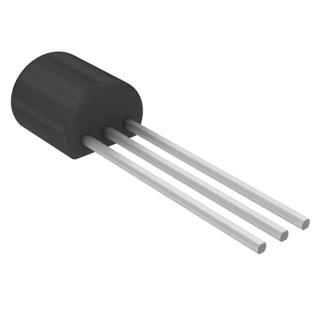
TOï92 (TOï226AA)
CASE 029
STYLE 12
MARKING DIAGRAM
Z0
10xMA
YWW G
G
1 2 3
x
= 3,7,9
Y
= Year
WW
= Work Week
G
= PbïFree Package
(*Note: Microdot may be in either location)
PIN ASSIGNMENT
1
Main Terminal 1
2
Gate
3
Main Terminal 2
ORDERING INFORMATION
See detailed ordering and shipping information in the package
dimensions section on page 6 of this data sheet.
© Semiconductor Components Industries, LLC, 2012
January, 2012 ï Rev. 0
1
Publication Order Number:
Z0107MA/D
�Z0107MA
THERMAL CHARACTERISTICS
Symbol
Max
Unit
Thermal Resistance, JunctionïtoïCase
Characteristic
RqJC
50
°C/W
Thermal Resistance, JunctionïtoïAmbient
RqJA
160
°C/W
TL
260
°C
Maximum Lead Temperature for Soldering Purposes for 10 Seconds
ELECTRICAL CHARACTERISTICS (TC = 25°C unless otherwise noted; Electricals apply in both directions)
Characteristic
Symbol
Min
Typ
Max
Unit
IDRM, IRRM
ï
ï
ï
ï
5.0
500
mA
Peak OnïState Voltage
(ITM = "1.4 A Peak; Pulse Width v 2.0 ms, Duty Cycle v 2.0%)
VTM
ï
ï
1.56
V
Gate Trigger Current (Continuous dc)
(VD = 12 Vdc, RL = 30 W)
MT2(+), G(+)
MT2(+), G(ï)
MT2(ï), G(ï)
MT2(ï), G(+)
IGT
OFF CHARACTERISTICS
Peak Repetitive Blocking Current
(VD = Rated VDRM, VRRM; Gate Open)
TJ = 25°C
TJ = +125°C
ON CHARACTERISTICS
Latching Current (VD = 12 V, IG = 1.2 x IGT)
MT2(+), G(+) All Types
MT2(+), G(ï) All Types
MT2(ï), G(ï) All Types
MT2(ï), G(+) All Types
IL
Gate Trigger Voltage (Continuous dc)
(VD = 12 Vdc, RL = 30 W)
MT2(+), G(+) All Types
MT2(+), G(ï) All Types
MT2(ï), G(ï) All Types
MT2(ï), G(+) All Types
VGT
Gate NonïTrigger Voltage
(VD = 12 V, RL = 30 W, TJ = 125°C)
All Four Quadrants
Holding Current
(VD = 12 Vdc, Initiating Current = 50 mA, Gate Open)
mA
0.15
0.15
0.15
0.25
ï
ï
ï
ï
5.0
5.0
5.0
7.0
ï
ï
ï
ï
ï
ï
ï
ï
10
20
10
10
mA
V
ï
ï
ï
ï
ï
ï
ï
ï
1.3
1.3
1.3
1.3
VGD
0.2
ï
1.3
V
IH
ï
ï
10
mA
di/dt(c)
1.6
ï
ï
A/ms
20
60
ï
ï
ï
20
DYNAMIC CHARACTERISTICS
Rate of Change of Commutating Current
(VD = 400 V, ITM = 0.84 A, Commutating dv/dt = 1.5 V/ms, Gate Open,
TJ = 110°C, f = 250 Hz, with Snubber)
Critical Rate of Rise of OffïState Voltage (VD = 67% Rated VDRM,
Exponential Waveform, Gate Open, TJ = 110°C)
dv/dt
Repetitive Critical Rate of Rise of OnïState Current, TJ = 125°C
Pulse Width = 20 ms, IPKmax = 15 A, diG/dt = 1 A/ms, f = 60 Hz
di/dt
http://onsemi.com
2
V/ms
A/ms
�Z0107MA
Voltage Current Characteristic of Triacs
(Bidirectional Device)
+ Current
Symbol
Parameter
VDRM
IDRM
Peak Repetitive Forward Off State Voltage
Peak Forward Blocking Current
VRRM
Peak Repetitive Reverse Off State Voltage
VTM
IRRM
Peak Reverse Blocking Current
VTM
Maximum On State Voltage
IH
Holding Current
on state
IRRM at VRRM
IH
Quadrant 3
MainTerminal 2 ï
IH
off state
VTM
Quadrant Definitions for a Triac
MT2 POSITIVE
(Positive Half Cycle)
+
(+) MT2
Quadrant II
(+) MT2
(ï) IGT
GATE
Quadrant I
(+) IGT
GATE
MT1
MT1
REF
REF
IGT ï
+ IGT
(ï) MT2
(ï) MT2
Quadrant III
Quadrant IV
(+) IGT
GATE
(ï) IGT
GATE
MT1
MT1
REF
REF
ï
MT2 NEGATIVE
(Negative Half Cycle)
All polarities are referenced to MT1.
With inïphase signals (using standard AC lines) quadrants I and III are used.
http://onsemi.com
3
Quadrant 1
MainTerminal 2 +
+ Voltage
IDRM at VDRM
�Z0107MA
110
100
100
I T(RMS) , MAXIMUM ALLOWABLE
AMBIENT TEMPERATURE ( °C)
T = 30°
60°
90
DC
90°
80
180°
70
120°
60
a
50
a
40
30
a = CONDUCTION ANGLE
0.1
0.2
0.3
60°
90
0.4
0.5
0.6
0.7
0.8
90°
DC
80
180°
70
120°
60
a
50
40
20
0
T = 30°
a
30
a = CONDUCTION ANGLE
0
0.05
0.1
0.15
0.2
0.25
0.3
IT(RMS), RMS ON-STATE CURRENT (AMPS)
IT(RMS), RMS ON-STATE CURRENT (AMPS)
Figure 1. RMS Current Derating
Figure 2. RMS Current Derating
1.2
0.35
0.4
5.2
6.0
6.0
4.0
a
1.0
DC
a
0.8
TJ = 110°C
180°
2.0
a = CONDUCTION ANGLE
25°C
120°
0.6
1.0
0.4
ITM, INSTANTANEOUS ON‐STATE CURRENT (AMP)
P(AV), MAXIMUM AVERAGE POWER DISSIPATION (WATTS)
TC, MAXIMUM ALLOWABLE CASE TEMPERATURE ( °C)
110
90°
60°
0.2
T = 30°
0
0
0.1
0.2
0.3
0.4
0.5
0.6
0.7
0.8
IT(RMS), RMS ON-STATE CURRENT (AMPS)
Figure 3. Power Dissipation
0.6
0.4
0.2
0.1
0.06
0.04
0.02
0.01
0.006
0.4
1.2
2.0
2.8
3.6
4.4
VTM, INSTANTANEOUS ON‐STATE VOLTAGE (VOLTS)
Figure 4. OnïState Characteristics
http://onsemi.com
4
�Z0107MA
10
I TSM , PEAK SURGE CURRENT (AMPS)
R(t), TRANSIENT THERMAL RESISTANCE (NORMALIZED)
1.
0
ZQJC(t) = RQJC(t) @ r(t)
0.1
0.01
0.1
1.0
10
1•103
100
5.0
3.0
TJ = 110°C
f = 60 Hz
2.0
Surge is preceded and followed by rated current.
1.0
1.0
1•104
2.0
3.0
5.0
t, TIME (ms)
10
30
50
100
NUMBER OF CYCLES
Figure 5. Transient Thermal Response
Figure 6. Maximum Allowable Surge Current
100
1.2
VGT, GATE TRIGGER VOLTAGE (V)
I GT , GATE TRIGGER CURRENT (mA)
CYCLE
Q4
10
Q3
Q2
Q1
1
1.1
Q4
1.0
Q3
0.9
Q2
0.8
Q1
0.7
0.6
0.5
0.4
0
-40 -25
-10
5
20
35
50
65
80
95
0.3
-40 -25
110
5
20
35
50
65
80
95
TJ, JUNCTION TEMPERATURE (°C)
TJ, JUNCTION TEMPERATURE (°C)
Figure 7. Typical Gate Trigger Current versus
Junction Temperature
Figure 8. Typical Gate Trigger Voltage versus
Junction Temperature
100
110
10
10
IH , HOLDING CURRENT (mA)
IL , LATCHING CURRENT (mA)
-10
Q2
Q3
Q4
1
Q1
0
-40 -25
-10
5
20
35
50
65
80
95
MT2 Negative
1
MT2 Positive
0.1
-40 -25
110
-10
5
20
35
50
65
80
95
TJ, JUNCTION TEMPERATURE (°C)
TJ, JUNCTION TEMPERATURE (°C)
Figure 9. Typical Latching Current versus
Junction Temperature
Figure 10. Typical Holding Current versus
Junction Temperature
http://onsemi.com
5
110
�Z0107MA
LL
200 VRMS
ADJUST FOR
ITM, 60 Hz VAC
1N4007
MEASURE
I
CHARGE
CONTROL
TRIGGER CONTROL
CHARGE
TRIGGER
NON‐POLAR
CL
RS
CS
MT2
1N914 51 W
ADJUST FOR +
di/dt(c)
200 V
MT1
G
Note: Component values are for verification of rated (di/dt)c. See AN1048 for additional information.
Figure 11. Simplified Test Circuit to Measure the Critical Rate of Rise of Commutating Current (di/dt)c
ORDERING & SHIPPING INFORMATION: Packaging Options, Device Suffix
U.S.
Europe
Equivalent
Z0107MARL1G
Shipping†
Description of TOï92 Tape Orientation
Radial Tape and Reel (2K/Reel)
Flat side of TOï92 and adhesive tape visible
Z0107MAG
Bulk in Box (5K/Box)
N/A, Bulk
Z0107MARLRPG
Radial Tape and Fan Fold Box (2K/Box)
Round side of TOï92 and adhesive tape visible
Z0107MARLRFG
Radial Tape and Fan Fold Box (2K/Box)
Round side of TOï92 and adhesive tape on reverse side
†For information on tape and reel specifications, including part orientation and tape sizes, please refer to our Tape and Reel Packaging
Specification Brochure, BRD8011/D.
http://onsemi.com
6
�Z0107MA
PACKAGE DIMENSIONS
TOï92 (TOï226AA)
CASE 029ï11
ISSUE AM
A
B
STRAIGHT LEAD
BULK PACK
R
P
L
SEATING
PLANE
K
D
X X
G
J
H
V
C
SECTION XïX
N
1
NOTES:
1. DIMENSIONING AND TOLERANCING PER ANSI
Y14.5M, 1982.
2. CONTROLLING DIMENSION: INCH.
3. CONTOUR OF PACKAGE BEYOND DIMENSION R
IS UNCONTROLLED.
4. LEAD DIMENSION IS UNCONTROLLED IN P AND
BEYOND DIMENSION K MINIMUM.
DIM
A
B
C
D
G
H
J
K
L
N
P
R
V
INCHES
MIN
MAX
0.175
0.205
0.170
0.210
0.125
0.165
0.016
0.021
0.045
0.055
0.095
0.105
0.015
0.020
0.500
--0.250
--0.080
0.105
--0.100
0.115
--0.135
---
MILLIMETERS
MIN
MAX
4.45
5.20
4.32
5.33
3.18
4.19
0.407
0.533
1.15
1.39
2.42
2.66
0.39
0.50
12.70
--6.35
--2.04
2.66
--2.54
2.93
--3.43
---
N
A
R
BENT LEAD
TAPE & REEL
AMMO PACK
B
P
T
SEATING
PLANE
G
K
D
X X
J
V
1
C
N
SECTION XïX
NOTES:
1. DIMENSIONING AND TOLERANCING PER
ASME Y14.5M, 1994.
2. CONTROLLING DIMENSION: MILLIMETERS.
3. CONTOUR OF PACKAGE BEYOND
DIMENSION R IS UNCONTROLLED.
4. LEAD DIMENSION IS UNCONTROLLED IN P
AND BEYOND DIMENSION K MINIMUM.
DIM
A
B
C
D
G
J
K
N
P
R
V
MILLIMETERS
MIN
MAX
4.45
5.20
4.32
5.33
3.18
4.19
0.40
0.54
2.40
2.80
0.39
0.50
12.70
--2.04
2.66
1.50
4.00
2.93
--3.43
---
STYLE 12:
PIN 1. MAIN TERMINAL 1
2. GATE
3. MAIN TERMINAL 2
ON Semiconductor and
are registered trademarks of Semiconductor Components Industries, LLC (SCILLC). SCILLC reserves the right to make changes without further notice
to any products herein. SCILLC makes no warranty, representation or guarantee regarding the suitability of its products for any particular purpose, nor does SCILLC assume any liability
arising out of the application or use of any product or circuit, and specifically disclaims any and all liability, including without limitation special, consequential or incidental damages.
“Typical” parameters which may be provided in SCILLC data sheets and/or specifications can and do vary in different applications and actual performance may vary over time. All
operating parameters, including “Typicals” must be validated for each customer application by customer’s technical experts. SCILLC does not convey any license under its patent rights
nor the rights of others. SCILLC products are not designed, intended, or authorized for use as components in systems intended for surgical implant into the body, or other applications
intended to support or sustain life, or for any other application in which the failure of the SCILLC product could create a situation where personal injury or death may occur. Should
Buyer purchase or use SCILLC products for any such unintended or unauthorized application, Buyer shall indemnify and hold SCILLC and its officers, employees, subsidiaries, affiliates,
and distributors harmless against all claims, costs, damages, and expenses, and reasonable attorney fees arising out of, directly or indirectly, any claim of personal injury or death
associated with such unintended or unauthorized use, even if such claim alleges that SCILLC was negligent regarding the design or manufacture of the part. SCILLC is an Equal
Opportunity/Affirmative Action Employer. This literature is subject to all applicable copyright laws and is not for resale in any manner.
PUBLICATION ORDERING INFORMATION
LITERATURE FULFILLMENT:
Literature Distribution Center for ON Semiconductor
P.O. Box 5163, Denver, Colorado 80217 USA
Phone: 303ï675ï2175 or 800ï344ï3860 Toll Free USA/Canada
Fax: 303ï675ï2176 or 800ï344ï3867 Toll Free USA/Canada
Email: orderlit@onsemi.com
N. American Technical Support: 800ï282ï9855 Toll Free
USA/Canada
Europe, Middle East and Africa Technical Support:
Phone: 421 33 790 2910
Japan Customer Focus Center
Phone: 81ï3ï5817ï1050
http://onsemi.com
7
ON Semiconductor Website: www.onsemi.com
Order Literature: http://www.onsemi.com/orderlit
For additional information, please contact your local
Sales Representative
Z0107MA/D
�


 工商网监
湘ICP备2023018690号
工商网监
湘ICP备2023018690号
