### 物料型号
- OPB825:Slotted Switch (no tabs)
- OPB825A:Slotted Switch (one tab)
- OPB825B:Slotted Switch (two tabs)
### 器件简介
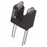
OPB825, OPB825A和OPB825B均由一个红外发射二极管和一个NPN硅光晶体管组成,它们被安装在一个低成本的黑色塑料封装中,相对放置在0.160”(4.064 mm)宽的槽的两侧。OPB825没有安装耳,适用于直接插入PCB板或双列直插式插座。OPB825A在光晶体管侧有一个安装耳,而OPB825B在两侧都有安装耳(两个耳)。
### 引脚分配
| Pin# | 描述 | Pin# | 描述 |
| --- | --- | --- | --- |
| 1 | 阳极 | 3 | 集电极 |
| 2 | 阴极 | 4 | 发射极 |
### 参数特性
- 绝对最大额定值:
- 存储和工作温度范围:-40°C至+85°C
- 引脚焊接温度:260°C(从外壳1/16英寸处焊接5秒)
- 输入二极管:
- 正向直流电流:50 mA
- 峰值正向电流(1 µs脉冲宽度,300 pps):3 A
- 反向直流电压:2 V
- 功率耗散:100 mW
- 输出光晶体管:
- 集电极-发射极电压:30 V
- 发射极-集电极电压:5 V
- 集电极直流电流:30 mA
- 功率耗散:100 mW
### 功能详解
光晶体管开关在任何不透明物体通过槽时都会发生。当物体通过时,红外发射二极管发出的光被阻断,导致光晶体管的集电极电流发生变化,从而实现开关功能。
### 应用信息
- 非接触式中断物体感应
- 装配线自动化
- 机器自动化
- 设备安全
- 机器安全
### 封装信息
这些器件被封装在一个低成本的黑色塑料外壳中,具有0.160”(4.064 mm)宽的槽和0.300”(7.62 mm)的引脚间距。