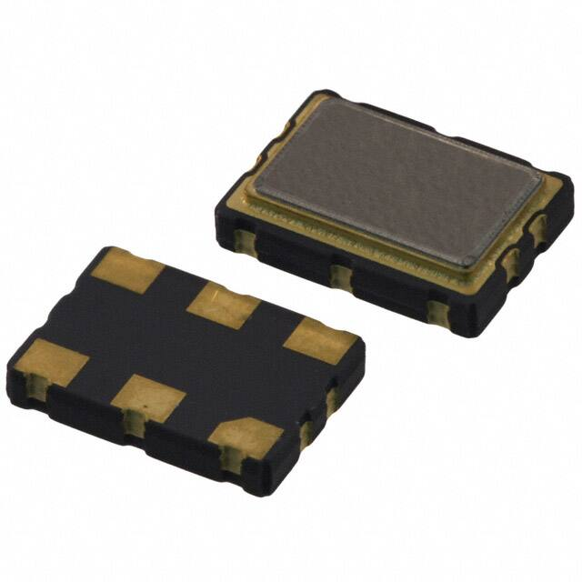
KC7050P150.000L20E00 数据手册
Clock Oscillators Surface Mount Type
KC7050P-L2/ KC7050P-L3 Series
LVDS/ 3.3V or 2.5V/ 7.0×5.0mm
Features
How to Order
KC7050P 125.000 L □ □ J 00
• Miniature ceramic package
• �Highly reliable with seam welding
• �LVDS output
• �Supply voltage VCC=3.3V, 2.5V
• �±25×10−6 available
• �Low Phase Noise
Table 1
Operating
Freq. Tol.
Temperature
Code × 10−6 Range (°C)
± 50
0
± 30 0 to +70
S
± 25
U
±100
F
−40 to +85
± 50
G
±
−40
6
50
to +105
RoHS Compliant
Note
Please contact
us for available
frequencies.
Conditions
Frequency Tolerance
f_tol
Storage Temperature Range
T_stg
Initial tolerance, Operating temperature range, Rated power supply voltage
change, Load change, Aging (1 year
@25°C), Shock and vibration
Output Frequency Range
fo
Note1
Operating Temperature Range
Phase Jitter
—
VCC
ICC
I_std
SYM
Tr/ Tf
VOL
VOH
VOD
dVOD
VOS
dVOS
RL
VIN
VIL
VIH
t_dis
t_ena
t_str
DJ
JSigma
JPK-PK
Standard Specifications
Extend (Option)
100ohm @crossing point
100ohm
Measured with Wavecrest SIA-3000
BW : 12kHz to 20MHz
(Unit: mm)
1.4
Unit
MHz
×10−6
°C
°C
V
V
mA
μA
%
ns
V
V
mV
mV
V
mV
ohm
V
V
V
ns
ms
ms
ps
ps
ps
0.3max.
ps
Recommended Land Pattern�
(Unit: mm)
5.08
#4
#5
#6
#3
#2
#1
1.17
2.54
1.6
KC7050P-L3
0.6
2.46
7.0
Specifications
0.9 min. Typ.:1.1
1.6 max. Typ.:1.43
247 to 454 Typ.:330
50 max.
1.125 to 1.375
50 max.
100
0 to VCC
30% VCC max.
70% VCC min.
200 max.
10 max.
10 max.
2 max.
4 max.
30 max.
@Minimum operating voltage to be 0 sec.
5.0
Dimensions�
Packaging (Tape & Reel 1000 pcs./ reel)
0.6 max.
dVOS=¦VOS1−VOS2¦
LVDS Output
@156.25MHz
VCC=3.3V
(STD Specification is “00”.)
25 to 175
±50/ −40 to +105°C
±100/ −40 to +85°C
±50/ −40 to +85°C
±50/ 0 to +70°C
±30/ 0 to +70°C
±25/ 0 to +70°C
−55 to +125
0 to +70/ −40 to +85
−40 to +105
−0.5 to +5.0
+2.375 to +2.625
+2.97 to +3.63
50 max.
20 max.
50±5
dVOD=¦VOD1−VOD2¦
JPhase
J : 45/ 55%
⑦��Individual Specification
KC7050P-L2
Note : �All electrical characteristics are defined at the maximum load and operating temperature range.
Note1: �Please contact us for inquiry about operating temperature range, available frequencies and other conditions.
Note2: �DC characteristic
0.75
Crystal Oscillators
Max. Supply Voltage
Supply Voltage
Current Consumption
Stand-by Current
Symmetry
Rise/ Fall Time
(20% VCC to 80% VCC Maximum
Loaded)
Low Level Output VoltageNote2
High Level Output VoltageNote2
Diffrentical Output VoltageNote2
Diffrentical Output Voltage ErrorNote2
Offset Voltage
Offset Voltage Error
Output Load
Input Voltage Range
Low Level Input Voltage
High Level Input Voltage
Disable Time
Enable Time
Start-up Time
Deterministic Jitter
1 Sigma Jitter
Peak to Peak Jitter
T_use
①Series
②Output Frequency
③Output Type (LVDS)
④Supply Voltage (3 : 3.3V or 2 : 2.5V)
⑤Frequency Tolerance (See Table 1)
⑥�Symmetry/ INH Function
Standard specifications
Symbol
③ ④ ⑤ ⑥ ⑦
2.54
Plating: Ni+Au
Tolerance: ±0.2
#1
#2
#3
#4
#5
#6
Pad Connections
INH
NC
Case GND
Output
Complementary Output
VCC
Pad1
Open
"H" Level
"L" Level
INH Function
Pad4/ Pad5 (Output)
Active
Active
High Z (No-Oscillation)
1.6
Item
②
3.6
Specifications
①
2.54
1.6
Note: 0.01µF and 10µF capacitor between Vcc and
GND is recommended for bypass purpose.
As of December 2019
�
KC7050P150.000L20E00 价格&库存
很抱歉,暂时无法提供与“KC7050P150.000L20E00”相匹配的价格&库存,您可以联系我们找货
免费人工找货