T-55923GD050J-LW-ABN 数据手册
�
Spec No.
Date
SPEC
TQ3C-8EAF0-E1YAW02-00
August 5, 2013
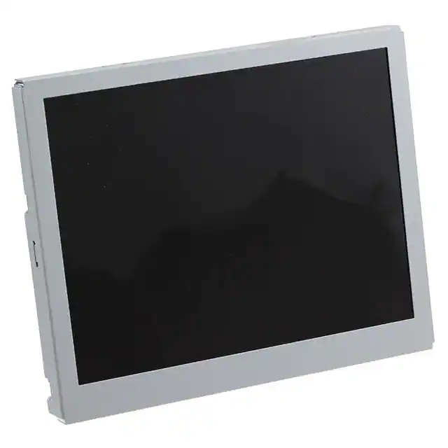
TYPE : T-55923GD050J-LW-ABN
(TCG050VGLP*ANN-AN*02)
< 5.0 inch VGA transmissive color TFT with LED backlight>
CONTENTS
1.
2.
3.
4.
5.
6.
7.
8.
9.
10.
11.
12.
13.
14.
Application
Construction and outline
Mechanical specifications
Absolute maximum ratings
Electrical characteristics
Optical characteristics
Interface signals
Input timing characteristics
Backlight characteristics
Lot number identification
Warranty
Precautions for use
Reliability test data
Outline drawing
KYOCERA DISPLAY CORPORATION
This specification is subject to change without notice.
Consult Kyocera before ordering.
� � �
Original
Issue Date
August 5, 2013
Designed by: Engineering dept.
Prepared
Checked
Confirmed by: QA dept.
Approved
Checked
Approved
�Spec No.
TQ3C-8EAF0-E1YAW02-00
Part No.
Page
T-55923GD050J-LW-ABN
Warning
1. This Kyocera LCD module has been specifically designed for use only in
electronic devices and industrial machines in the area of audio control,
office automation, industrial control, home appliances, etc. The module
should not be used in applications where the highest level of safety and
reliability are required and module failure or malfunction of such module
results in physical harm or loss of life, as well as enormous damage or loss.
Such fields of applications include, without limitation, medical, aerospace,
communications infrastructure, atomic energy control. Kyocera expressly
disclaims any and all liability resulting in any way to the use of the module
in such applications.
2. Customer agrees to indemnify, defend and hold Kyocera harmless
from and against any and all actions, claims, damages, liabilities,
awards, costs, and expenses, including legal expenses, resulting from or
arising out of Customer's use, or sale for use, or Kyocera modules in
applications.
Caution
1. Kyocera shall have the right, which Customer hereby acknowledges, to
immediately scrap or destroy tooling for Kyocera modules for which no
Purchase Orders have been received from the Customer in a two-year period.
-
�Spec No.
Part No.
TQ3C-8EAF0-E1YAW02-00
Revision record
Designed by : Engineering dept.
Date
Rev.No.
Prepared
Date
Page
Checked
Approved
Page
T-55923GD050J-LW-ABN
Confirmed by : QA dept.
Checked
Descriptions
Approved
-
�Spec No.
Part No.
TQ3C-8EAF0-E1YAW02-00
Page
T-55923GD050J-LW-ABN
1
1. Application
This document defines the specification of T-55923GD050J-LW-ABN.
(RoHS Compliant)
2. Construction and outline
LCD
Backlight system
Polarizer
Additional circuit
: Transmissive color dot matrix type TFT
: LED
: Glare treatment
: Timing controller, Power supply (3.3V input)
(without constant current circuit for LED Backlight)
3. Mechanical specifications
Item
Specification
Unit
98.0(W)×119.0(H)×10.5(D)
mm
Active area
76.32(W)×101.76(H)
(12.72cm/5.0 inch(Diagonal))
mm
Dot format
480(W)640×(R,G,B)(H)
dot
0.159(W)×0.053(H)
mm
Normally White
-
185
g
Outline dimensions 1)
Dot pitch
Base color
Mass
2)
1) Projection not included. Please refer to outline for details.
2) Due to the characteristics of the LCD material, the color varies with environmental temperature.
M407011� � � � � � � � � � � � � � � � � � � � � � � � � � � � � � � �
�Spec No.
Part No.
TQ3C-8EAF0-E1YAW02-00
Page
T-55923GD050J-LW-ABN
2
4. Absolute maximum ratings
4-1. Electrical absolute maximum ratings
Item
Supply voltage
Symbol
Min.
Max.
Unit
VDD
(-0.3)
(4.0)
V
Input signal voltage
1)
VIN
(0)
(VDD)
V
LED forward current
2) 3)
IF
-
(70)
mA
1) Input signal : DCLK, R0㹼R7, G0㹼G7, B0㹼B7, HD, VD, DENA
2) For each “AN-CA”
3) Do not apply reversed voltage.
4-2. Environmental absolute maximum ratings
Item
Symbol
Min.
Max.
Unit
Operating temperature
1)
TOP
(-30)
(80)
°C
Storage temperature
2)
TSTO
(-30)
(80)
°C
Operating humidity
3)
HOP
(10)
4)
%RH
Storage humidity
3)
HSTO
(10)
4)
%RH
Vibration
-
5)
5)
-
Shock
-
6)
6)
-
1) Operating temperature means a temperature which operation shall be guaranteed. Since display
performance is evaluated at 25°C, another temperature range should be confirmed.
2) Temp. = (-30)°C㸺(48)h , Temp. = (80)°C㸺(168)h
� � � Store LCD at normal temperature/humidity. Keep them free from vibration and shock.
An LCD that is kept at a low or a high temperature for a long time can be defective due to
other conditions, even if the low or high temperature satisfies the standard.
� (Please refer to “Precautions for Use” for details.)
3) Non-condensing
4) Temp.ӌ(40)°C, (85)%RH Max.
� � Temp.㸼(40)°C, Absolute humidity shall be less than (85)%RH at (40)°C.
� 5)� Vibration level 9.8m/s2(1.0G)�
Waveform : sinusoidal
Frequency range : 5 to 500Hz
� � � � Frequency sweep rate : 0.5 octave/min
� � � � Duration : one sweep from 5to 500Hz in each of three mutually perpendicular axis(total 3 hours)
6) Acceleration: 1,470 m/s2(150G), Waveform : half sinusoidal wave 2ms
3 times in each direction: ±X, ±Y, ±Z
� �
M407011� � � � � � � � � � � � � � � � � � � � � � � � � � � � � � � �
�Spec No.
Part No.
TQ3C-8EAF0-E1YAW02-00
Page
T-55923GD050J-LW-ABN
3
5. Electrical characteristics
� � � � � � � � � � � � �
Item
Temp. = (-30)㹼(80)°C
� � � �
Symbol
Condition
Min.
Typ.
Max.
Unit
VDD
-
3.0
3.3
3.6
V
Current consumption
IDD
2)
-
(29.0)
(34.0)
mA
Permissive input ripple voltage
VRP
-
-
-
(TBD)
mVp-p
VIL
"Low" level
(0)
-
(0.3VDD)
V
VIH
"High" level
(0.7VDD)
-
(VDD)
V
Supply voltage
1)
Input signal voltage
3)
1) VDD-turn-on conditions
3.0V
� � � � � � � � � � � �
� � � � � � � � � � � � �
0.3V
� � � � � � � � � � � � �
t1
t2
3.0V
� � � � � � � � � � � � � � � �
� � � � � � � � � � � � � � � �
Signal 3)
� � � � � � � � � � � � � � � �
� � � �
� � � �
� � �
� �
�
�
(TBD)㸺t1ӌ(TBD)ms
�
(TBD)㸺t2ӌ(TBD)ms
(TBD)㸺t3ӌ(TBD)s
t3
2) Display pattern:
VDD = 3.3V, Temp. = 25°C
123 456 789 ࣭࣭࣭࣭࣭࣭࣭࣭࣭࣭࣭࣭࣭1918 1919 1920(dot)
� 1 ڧڧڧڧڧڧڧڧڧڧڧڧڧڧڧڧڧڧڧڧڧ
2 ڧڧڧڧڧڧڧڧڧڧڧڧڧڧڧڧڧڧڧڧڧ
3 ڧڧڧڧڧڧڧڧڧڧڧڧڧڧڧڧڧڧڧڧڧ
: ڧڧڧڧڧڧڧڧڧڧڧڧڧڧڧڧڧڧڧڧڧ
: ڧڧڧڧڧڧڧڧڧڧڧڧڧڧڧڧڧڧڧڧڧ
: ڧڧڧڧڧڧڧڧڧڧڧڧڧڧڧڧڧڧڧڧڧ
479 ڧڧڧڧڧڧڧڧڧڧڧڧڧڧڧڧڧڧڧڧڧ
480 ڧڧڧڧڧڧڧڧڧڧڧڧڧڧڧڧڧڧڧڧڧ
(dot)
3) Input signal : DCLK, R0㹼R7, G0㹼G7, B0㹼B7, HD, VD, DENA
M407011� � � � � � � � � � � � � � � � � � � � � � � � � � � � � � � �
�Spec No.
Part No.
TQ3C-8EAF0-E1YAW02-00
Page
4
T-55923GD050J-LW-ABN
6. Optical characteristics
� � � � � � � � � � �
Item
Response time
Measuring spot =ȭ6.0mm, Temp. = 25°C
� � � � � � � �
Symbol
Condition
Min.
Typ.
Max.
Unit
Rise
Ǖr
ȟ=ȭ=0°
-
(4)
-
ms
Down
Ǖd
ȟ=ȭ=0°
-
(12)
-
ms
ȟUPPER
-
(50)
-
ȟLOWER
-
(60)
-
-
(70)
-
-
(70)
-
Viewing angle range
View direction
: 6 o’clock
(Gray inversion)
CRӍ10
ȭLEFT
䃥RIGHT
Contrast ratio
Brightness
ȟ=ȭ=0°
(350)
(500)
-
-
L
IF=60mA/Line
(600)
(800)
-
cd/m2
(0.509)
(0.549)
(0.589)
(0.316)
(0.356)
(0.396)
(0.299)
(0.339)
(0.379)
(0.499)
(0.539)
(0.579)
(0.114)
(0.154)
(0.194)
(0.090)
(0.130)
(0.170)
(0.273)
(0.313)
(0.353)
(0.289)
(0.329)
(0.369)
y
x
Green
y
Chromaticity
coordinates
x
Blue
y
x
White
y
ȟ=ȭ=0°
ȟ=ȭ=0°
ȟ=ȭ=0°
ȟ=ȭ=0°
6-1. Definition of contrast ratio
CR(Contrast ratio) 㸻
Brightness with all pixels "White"
Brightness with all pixels "Black"
6-2. Definition of response time
:KLWH
%ODFN
���
���
���
����
%ULJKWQHVV
:KLWH
ȫU
deg.
CR
x
Red
deg.
ȫG
M407011� � � � � � � � � � � � � � � � � � � � � � � � � � � � � � � �
-
�Spec No.
Part No.
TQ3C-8EAF0-E1YAW02-00
Page
5
T-55923GD050J-LW-ABN
6-3. Definition of viewing angle
ȭ �r
ȟ833(5
�\
ȟ �r
�\
ȟ/2:(5
ȭ/()7
�[
�[
ȭ5,*+7
�[
�[
�\
ȟ�GLUHFWLRQ
�\
ȭ�GLUHFWLRQ
6-4. Brightness measuring points
1) Rating is defined as the white brightness at center of display screen(3).
2) 5 minutes after LED is turned on. (Ambient Temp.=25Υ)
M407011� � � � � � � � � � � � � � � � � � � � � � � � � � � � � � � �
�Spec No.
TQ3C-8EAF0-E1YAW02-00
Part No.
Page
T-55923GD050J-LW-ABN
6
7. Interface signals
7-1. Interface signals
No.
Symbol
Description
� GND
1
GND
2
DCLK � Clock signal for sampling each data signal
� GND
3
GND
� Horizontal synchronous signal
4
HD
� Vertical synchronous signal
5
VD
� GND
6
GND
� RED data signal (LSB)
7
R0
� RED data signal
8
R1
� RED data signal
9
R2
RED data signal
10
R3
RED data signal
11
R4
� RED data signal
12
R5
� RED data signal
13
R6
RED data signal (MSB)
14
R7
� GND
15
GND
� GREEN data signal (LSB)
16
G0
� GREEN data signal
17
G1
� GREEN data signal
18
G2
� GREEN data signal
19
G3
� GREEN data signal
20
G4
� GREEN data signal
21
G5
� GREEN data signal
22
G6
� GREEN data signal (MSB)
23
G7
� GND
24
GND
� BLUE data signal (LSB)
25
B0
� BLUE data signal
26
B1
� BLUE data signal
27
B2
� BLUE data signal
28
B3
� BLUE data signal
29
B4
� BLUE data signal
30
B5
� BLUE data signal
31
B6
� BLUE data signal (MSB)
32
B7
33
GND
� GND
34
DENA � Signal to settle the horizontal display position
35
NC
No connect
36
VDD
3.3V power supply
37
VDD
3.3V power supply
38
NC
No connect
39
NC
No connect
40
SC
Scan direction control
41
NC
No connect
42
CA1
Cathode 1
43
CA2
Cathode 2
44
AN2
Anode 2
45
AN1
Anode 1
� � LCD connector
㸸 FH33-45S-0.5SH(10) (HIROSE)
� � Recommended FFC or FPC
㸸 0.5mm pitch
M407011� � � � � � � � � � � � � � � � � � � � � � � � � � � � � � � �
I/O
I
I
I
I
I
I
I
I
I
I
I
I
I
I
I
I
I
I
I
I
I
I
I
I
I
I
I
I
I
-
Note
1)
2)
�Spec No.
TQ3C-8EAF0-E1YAW02-00
Part No.
T-55923GD050J-LW-ABN
1)
Page
7
The horizontal display start timing is settled in accordance with a rising timing of ENAB signal.
In case ENAB is fixed "Low", the horizontal start timing is determined.
Don't keep ENAB "High" during operation.
2)� TBD
7-2. Test Pad
TEST
PAD� No.
Interface� Signal
No.
Symbol
1
14
R7(MSB)
2
3
4
5
6
7
8
9
10
11
12
13
1
23
2
32
4
34
5
36
42
43
44
45
GND
G7(MSB)
DCLK
B7(MSB)
HD
DENA
VD
VDD
CA1
CA2
AN2
AN1
M407011� � � � � � � � � � � � � � � � � � � � � � � � � � � � � � � �
�Spec No.
Part No.
TQ3C-8EAF0-E1YAW02-00
Page
T-55923GD050J-LW-ABN
8. Input timing characteristics
8-1. Timing characteristics
1) Horizontal timing
Parameter
Horizontal Display Area
DCLK frequency
One Horizontal Line
HS pulse width
HS Back Porch (Blanking)
HS Front Porch
DE mode Blanking
Symbol
thd
fclk
th
thpw
thb
thfp
th-thd
Min.
㻌
1
1
85
Spec.
Typ.
640
24
760
48
88
32
120
Max.
50
㻌
255
255
512
Unit
DCLK
MHz
DCLK
DCLK
DCLK
DCLK
DCLK
2) Vertical timing
Parameter
Vertical Display Area
VS period time
VS pulse width
VS Back Porch (Blanking)
VS Front Porch
DE mode Blanking
Symbol
tvd
tv
tvpw
tvb
tvfp
tv-tvd
Min.
513
3
1
4
Spec.
Typ.
480
525
3
32
13
45
Max.
767
255
255
255
8-2. Input Data Signals and Display position on the screen
�
M407011� � � � � � � � � � � � � � � � � � � � � � � � � � � � � � � �
Unit
TH
TH
TH
TH
TH
TH
8
�Spec No.
TQ3C-8EAF0-E1YAW02-00
Part No.
T-55923GD050J-LW-ABN
8-3. Input timing characteristics
1) Horizontal timing
2) Horizontal timing
M407011� � � � � � � � � � � � � � � � � � � � � � � � � � � � � � � �
Page
9
�Spec No.
Part No.
TQ3C-8EAF0-E1YAW02-00
Page
10
T-55923GD050J-LW-ABN
9. Backlight characteristics
Item
Forward current
Forward voltage
Operating life time
1)
1)
2), 3)
Symbol
Min.
Typ.
Max.
Unit
Note
IF
-
(60)
-
mA
Ta=-30㹼80°C
-
(19.7)
(21.6)
V
IF=60mA, Ta=-30Υ
-
(18.4)
(20.4)
V
IF=60mA, Ta=25Υ
-
(17.8)
(19.7)
V
IF=60mA, Ta=80Υ
-
(50,000)
-
h
IF=60mA, Ta=25Υ
VF
T
1) For each “AN-CA”
2) When brightness decrease 50% of minimum brightness.
The average life of a LED will decrease when the LCD is operating at higher temperatures.
3) Life time is estimated data.(Condition : IF=60mA, Ta=25Υ in chamber).
4) An input current below 15mA may reduce the brightness uniformity of the LED backlight.
This
is because the amount of light from each LED chip is different. Therefore, please evaluate carefully
before finalizing the input current.
�
M407011� � � � � � � � � � � � � � � � � � � � � � � � � � � � � � � �
�Spec No.
TQ3C-8EAF0-E1YAW02-00
Part No.
T-55923GD050J-LW-ABN
Page
11
10. Lot number identification
� The production lot number is specified as follows.
ڧڧ ڧ – ڧ ڧ ڧ ڧ ڧڧ
� � � � � � � � � � � � � � � � � � Factory Control Number(ᕤሙ⟶⌮␒ྕ)㸦0㹼99㸧
Data of the Week(〇㐀᭙᪥)(A㹼G)
Factory Number(ศᕤሙ␒ྕ)(0㹼9)
Factory Code(ᕤሙグྕ)(Alphabet)
Production Week(〇㐀㐌)(1㹼5)
Production Month(〇㐀᭶)(1㹼9, X, Y, Z)
Production year(〇㐀ᖺ)(Lowe 2 digits / すᬺᖺᩘୗ 2 ᱆)
11. Warranty
� 11-1. Incoming inspection
� � Please inspect the LCD within one month after your receipt.
�
� 11-2. Production warranty
� � Kyocera warrants its LCD’s for a period of 12 months from the ship date. Kyocera shall, by mutual
agreement, replace or re-work defective LCD’s that are shown to be Kyocera’s responsibility.
M407011� � � � � � � � � � � � � � � � � � � � � � � � � � � � � � � �
�Spec No.
TQ3C-8EAF0-E1YAW02-00
Part No.
Page
T-55923GD050J-LW-ABN
12
12. Precautions for use
12-1. Installation of the LCD
1) Please ground either of the mounting (screw) holes located at each corner of an LCD,
in order to stabilize brightness and display quality.
2) A transparent protection plate shall be added to protect the LCD and its polarizer
3) The LCD shall be installed so that there is no pressure on the LSI chips.
4) The LCD shall be installed flat, without twisting or bending.
5) A transparent protection sheet is attached to the polarizer. Please remove the protection film
slowly before use, paying attention to static electricity.
12-2. Static electricity
1) Since CMOS ICs are mounted directly onto the LCD glass, protection from static electricity is
required.
2) Workers should use body grounding. Operator should wear ground straps.
12-3. LCD operation
1) The LCD shall be operated within the limits specified. Operation at values outside of these limits
may shorten life, and/or harm display images.
12-4. Storage
1) The LCD shall be stored within the temperature and humidity limits specified.
Store in a dark area, and protect the LCD from direct sunlight or fluorescent light.
2) Always store the LCD so that it is free from external pressure onto it.
12-5. Usage
1) DO NOT store in a high humidity environment for extended periods. Polarizer degradation bubbles,
and/or peeling off of the polarizer may result.
2) The front polarizer is easily scratched or damaged. Prevent touching it with any hard material, and
from being pushed or rubbed.
3) The LCD screen may be cleaned by wiping the screen surface with a soft cloth or cotton pad using a
little Ethanol.
4) Water may cause damage or discoloration of the polarizer. Clean condensation or moisture from
any source immediately.
5) Always keep the LCD free from condensation during testing. Condensation may permanently spot
or stain the polarizer.
6) Do not disassemble LCD because it will result in damage.
7) This Kyocera LCD has been specifically designed for use in general electronic devices, but not
for use in a special environment such as usage in an active gas. Hence, when the LCD is supposed
to be used in a special environment, evaluate the LCD thoroughly beforehand and do not expose
the LCD to chemicals such as an active gas.
8) Please do not use solid-base image pattern for long hours because a temporary afterimage may
appear. We recommend using screen saver etc. in cases where a solid-base image pattern must
be used.
9) Liquid crystal may leak when the LCD is broken. Be careful not to let the fluid go into your eyes
and mouth. In the case the fluid touches your body; rinse it off right away with water and soap.
M407011� � � � � � � � � � � � � � � � � � � � � � � � � � � � � � � �
�Spec No.
Part No.
TQ3C-8EAF0-E1YAW02-00
Page
T-55923GD050J-LW-ABN
13. Reliability test data
� �
Test item
Test condition
Test time
High temp.
atmosphere
80°C
240h
Display function
Display quality
: No defect
: No defect
-30°C
240h
Display function
Display quality
: No defect
: No defect
40°C 90% RH
240h
Display function
Display quality
: No defect
: No defect
Temp. cycle
-30°C 1.0h
80°C 0.5h
100cycles
Display function
Display quality
: No defect
: No defect
High temp.
operation
80°C
240h
Display function
Display quality
: No defect
: No defect
10 times at 1
sec interval
Display function
Display quality
: No defect
: No defect
10 times at 1
sec interval
Display function
Display quality
: No defect
: No defect
Low temp.
atmosphere
High temp.
humidity
atmosphere
ESD
ESD
1)
2)
3)
4)
� �
Contact discharge
(Operation)
150pF, 330Ȑ,s8kV
Signal pin discharge
(Non-operation)
200pF,0Ȑ,s200V
Judgement
Each test item uses a test LCD only once. The tested LCD is not used in any other tests.
The LCD is tested in circumstances in which there is no condensation.
The reliability test is not an out-going inspection.
The result of the reliability test is for your reference purpose only.
The reliability test is conducted only to examine the LCD's capability.
M407011� � � � � � � � � � � � � � � � � � � � � � � � � � � � � � � �
13
��Spec No.
Date
TQ3C-8EAF0-E2YAW02-00
August 5, 2013
KYOCERA INSPECTION STANDARD
TYPE : T-55923GD050J-LW-ABN
(TCG050VGLP*ANN-AN*02)
KYOCERA DISPLAY CORPORATION
Original
Issue Date
Designed by : Engineering dept.
Prepared
Checked
Confirmed by : QA dept.
Approved
Checked
Approved
August 5, 2013
� � � � � � � � � � � � � � � � � � � � � � � � � � � � � � � � � � � � � � �
�
�Spec No.
Part No.
TQ3C-8EAF0-E2YAW02-00
Date
Revision record
Designed by : Engineering dept.
Prepared
Checked
Approved
Confirmed by : QA dept.
Checked
August 5, 2013
Rev.No.
Date
Page
Page
T-55923GD050J-LW-ABN
Descriptions
Approved
-
�Spec No.
�
�
Part No.
TQ3C-8EAF0-E2YAW02-00
Page
7������*'���-�/:�$%1
1
�
Visuals specification
1) Note
Note
General
1.
Customer identified anomalies not defined within this inspection standard shall be
reviewed by Kyocera, and an additional standard shall be determined by mutual
consent.
2.
This inspection standard about the image quality shall be applied to any defect within
the active area and shall not be applicable to outside of the area.
3.
Inspection conditions
Luminance
: 300㹼500 Lux min.
Inspection distance
: 350 mm.
Temperature
: Approximate 25Υ
Direction� � � � � �
: Normal to the LCD panel s10rhorizontal and
vertical
Definition of
Dot defect
Bright dot defect
inspection item
The dot is constantly “on” when power applied to the
LCD, even when all “Black” data sent to the screen.
Inspection tool: 5% Transparency neutral density filter.
Count dot: If the dot is visible through the filter.
Don’t count dot: If the dot is not visible through the
filter.
䠮 䠣 䠞 䠮 䠣 䠞 䠮 䠣 䠞
䠮 䠣 䠞 䠮 䠣 䠞 䠮 䠣 䠞
dot defect
䠮 䠣 䠞 䠮 䠣 䠞 䠮 䠣 䠞
Black dot defect
�
The dot is constantly “off” when power applied to the
LCD, even when all “White” data sent to the screen.
Adjacent dot
Adjacent dot defect is defined as two or more bright dot
defects or black dot defects.
䠮 䠣 䠞 䠮 䠣 䠞 䠮 䠣 䠞
䠮 䠣 䠞 䠮 䠣 䠞 䠮 䠣 䠞
䠮 䠣 䠞 䠮 䠣 䠞 䠮 䠣 䠞
Definition
Definition of circle size
dot defect
��
Definition of linear size
of size
ȍ㸻(㹟㸩㹠)/2
�����������������������������������������������������������������������
�
�Spec No.
�
�
Part No.
TQ3C-8EAF0-E2YAW02-00
Page
7������*'���-�/:�$%1
2
�
2) Standard
Defect Type
Visual defect
Scratch
Limit
0.01 mm < W ӌ 0.05 mm
N ӌ 4
L ӌ 10 mm
0.01 mm < W
N=0
10mm < L
Dent
Black spot bubble
Lint
0.05 mm < W
N=0
0.2 mm < ȍ ӌ 0.4 mm
N ӌ 4
0.4 mm < ȍ
N=0
0.2 mm < ȍ ӌ 0.4 mm
N ӌ 5
0.4 mm < ȍ
N=0
L ӌ 3 mm
N ӌ 4
W ӌ 0.1 mm
3 mm ӌ L
N=0
W ӌ 0.1 mm
0.1 mm < W
Electrical defect
Bright dot
N ӌ 5
Dark dot
N ӌ 5
Total dot
N ӌ 8
According to Black spot
Two adjacent dot
Bright dot
ӌ 2 pairs
Dark dot
ӌ 2 pairs
Three or more
Not allowed
adjacent dot
Line defect
Moire
Not allowed
All Moire is out of inspection.
�����������������������������������������������������������������������
�
�