PD - 97195
IRFB4020PbF
DIGITAL AUDIO MOSFET
Features
• Key parameters optimized for Class-D audio
amplifier applications
• Low RDSON for improved efficiency
• Low QG and QSW for better THD and improved
efficiency
• Low QRR for better THD and lower EMI
Key Parameters
VDS
RDS(ON) typ. @ 10V
Qg typ.
Qsw typ.
RG(int) typ.
TJ max
200
80
18
6.7
3.2
175
V
m:
nC
nC
Ω
°C
• 175°C operating junction temperature for
ruggedness
D
• Can deliver up to 300W per channel into 8Ω load in
half-bridge configuration amplifier
G
S
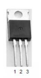
TO-220AB
Description
This Digital Audio MOSFET is specifically designed for Class-D audio amplifier applications. This MOSFET utilizes
the latest processing techniques to achieve low on-resistance per silicon area. Furthermore, Gate charge, body-diode
reverse recovery and internal Gate resistance are optimized to improve key Class-D audio amplifier performance
factors such as efficiency, THD and EMI. Additional features of this MOSFET are 175°C operating junction
temperature and repetitive avalanche capability. These features combine to make this MOSFET a highly efficient,
robust and reliable device for ClassD audio amplifier applications.
Absolute Maximum Ratings
Parameter
VDS
VGS
ID @ TC = 25°C
ID @ TC = 100°C
IDM
PD @TC = 25°C
PD @TC = 100°C
TJ
TSTG
Max.
Units
Drain-to-Source Voltage
200
V
Gate-to-Source Voltage
Continuous Drain Current, VGS @ 10V
Continuous Drain Current, VGS @ 10V
Pulsed Drain Current
±20
18
A
Power Dissipation
Power Dissipation
100
52
W
0.70
-55 to + 175
W/°C
°C
f
f
13
52
c
Linear Derating Factor
Operating Junction and
Storage Temperature Range
Soldering Temperature, for 10 seconds
(1.6mm from case)
Mounting torque, 6-32 or M3 screw
300
x
x
10lb in (1.1N m)
Thermal Resistance
f
Parameter
RθJC
Junction-to-Case
RθCS
RθJA
Case-to-Sink, Flat, Greased Surface
Junction-to-Ambient
f
Typ.
–––
0.50
Max.
1.43
–––
–––
62
Units
°C/W
Notes through
are on page 2
www.irf.com
1
03/03/06
�IRFB4020PbF
Electrical Characteristics @ TJ = 25°C (unless otherwise specified)
Parameter
Min.
Typ. Max. Units
Conditions
BVDSS
Drain-to-Source Breakdown Voltage
200
–––
–––
∆ΒVDSS/∆TJ
RDS(on)
VGS(th)
Breakdown Voltage Temp. Coefficient
Static Drain-to-Source On-Resistance
–––
–––
0.23
80
–––
100
Gate Threshold Voltage
Gate Threshold Voltage Coefficient
3.0
–––
–––
-13
4.9
–––
Drain-to-Source Leakage Current
–––
–––
–––
–––
20
250
µA
VDS = 200V, VGS = 0V
VDS = 200V, VGS = 0V, TJ = 125°C
IGSS
Gate-to-Source Forward Leakage
Gate-to-Source Reverse Leakage
–––
–––
–––
–––
100
-100
nA
VGS = 20V
VGS = -20V
gfs
Forward Transconductance
Total Gate Charge
24
–––
–––
18
–––
29
S
VDS = 50V, ID = 11A
Pre-Vth Gate-to-Source Charge
Post-Vth Gate-to-Source Charge
–––
–––
4.5
1.4
–––
–––
Gate-to-Drain Charge
Gate Charge Overdrive
Switch Charge (Qgs2 + Qgd)
–––
–––
5.3
6.8
–––
–––
Internal Gate Resistance
–––
–––
6.7
3.2
–––
–––
Turn-On Delay Time
Rise Time
–––
–––
7.8
12
–––
–––
Turn-Off Delay Time
Fall Time
–––
–––
16
6.3
–––
–––
Input Capacitance
Output Capacitance
–––
–––
1200
91
–––
–––
Reverse Transfer Capacitance
Effective Output Capacitance
–––
–––
20
110
–––
–––
ƒ = 1.0MHz,
See Fig.5
VGS = 0V, VDS = 0V to 160V
Internal Drain Inductance
–––
4.5
–––
Between lead,
∆VGS(th)/∆TJ
IDSS
Qg
Qgs1
Qgs2
Qgd
Qgodr
Qsw
RG(int)
td(on)
tr
td(off)
tf
Ciss
Coss
Crss
Coss eff.
LD
V
e
V VDS = VGS, ID = 100µA
mV/°C
nC
Internal Source Inductance
–––
7.5
VDS = 100V
VGS = 10V
ID = 11A
See Fig. 6 and 18
Ω
�e
VDD = 100V, VGS = 10V
ID = 11A
ns
RG = 2.4Ω
pF
VGS = 0V
VDS = 50V
nH
LS
VGS = 0V, ID = 250µA
V/°C Reference to 25°C, ID = 1mA
mΩ VGS = 10V, ID = 11A
–––
D
6mm (0.25in.)
from package
G
and center of die contact
S
Avalanche Characteristics
Parameter
EAS
IAR
EAR
Single Pulse Avalanche Energy
Avalanche Current
�g
Repetitive Avalanche Energy
Typ.
d
Max.
Units
–––
94
See Fig. 14, 15, 16a, 16b
g
mJ
A
mJ
Diode Characteristics
Parameter
IS @ TC = 25°C Continuous Source Current
Min.
Typ. Max. Units
–––
–––
18
ISM
(Body Diode)
Pulsed Source Current
–––
–––
52
VSD
(Body Diode)
Diode Forward Voltage
–––
–––
1.3
trr
Qrr
�c
Conditions
MOSFET symbol
A
V
Reverse Recovery Time
–––
82
120
ns
Reverse Recovery Charge
–––
280
420
nC
showing the
integral reverse
p-n junction diode.
TJ = 25°C, IS = 11A, VGS = 0V
TJ = 25°C, IF = 11A
di/dt = 100A/µs
e
e
Notes:
Repetitive rating; pulse width limited by max. junction temperature.
Starting TJ = 25°C, L = 1.62mH, RG = 25Ω, IAS = 11A.
Pulse width ≤ 400µs; duty cycle ≤ 2%.
2
Rθ is measured at TJ of approximately 90°C.
Limited by Tjmax. See Figs. 14, 15, 17a, 17b for repetitive
avalanche information.
www.irf.com
�IRFB4020PbF
100
100
10
BOTTOM
TOP
ID, Drain-to-Source Current (A)
ID, Drain-to-Source Current (A)
TOP
VGS
15V
12V
10V
8.0V
7.0V
6.0V
5.5V
5.0V
1
0.1
5.0V
10
BOTTOM
VGS
15V
12V
10V
8.0V
7.0V
6.0V
5.5V
5.0V
5.0V
1
≤60µs PULSE WIDTH
≤60µs PULSE WIDTH
Tj = 175°C
Tj = 25°C
0.1
0.01
0.1
1
10
0.1
100
100
3.5
VDS = 25V
≤60µs PULSE WIDTH
T J = 175°C
10
1
T J = 25°C
ID = 11A
VGS = 10V
3.0
2.5
(Normalized)
RDS(on) , Drain-to-Source On Resistance
100
ID, Drain-to-Source Current (A)
10
Fig 2. Typical Output Characteristics
Fig 1. Typical Output Characteristics
2.0
1.5
1.0
0.5
0.0
0.1
2
3
4
5
6
7
T J , Junction Temperature (°C)
Fig 3. Typical Transfer Characteristics
10000
Fig 4. Normalized On-Resistance vs. Temperature
12.0
VGS = 0V,
f = 1 MHZ
Ciss = C gs + C gd, C ds SHORTED
Crss = C gd
VGS, Gate-to-Source Voltage (V)
ID= 11A
Coss = C ds + C gd
Ciss
1000
-60 -40 -20 0 20 40 60 80 100120140160180
8
VGS, Gate-to-Source Voltage (V)
C, Capacitance (pF)
1
V DS, Drain-to-Source Voltage (V)
V DS, Drain-to-Source Voltage (V)
Coss
100
Crss
10.0
VDS= 160V
VDS= 100V
VDS= 40V
8.0
6.0
4.0
2.0
0.0
10
1
10
100
1000
VDS, Drain-to-Source Voltage (V)
Fig 5. Typical Capacitance vs.Drain-to-Source Voltage
www.irf.com
0
5
10
15
20
QG, Total Gate Charge (nC)
Fig 6. Typical Gate Charge vs.Gate-to-Source Voltage
3
�IRFB4020PbF
1000
T J = 175°C
10
T J = 25°C
1
OPERATION IN THIS AREA
LIMITED BY R DS(on)
100
ID, Drain-to-Source Current (A)
ISD, Reverse Drain Current (A)
100
10
1
100µsec
0.1
Tc = 25°C
Tj = 175°C
Single Pulse
0.01
VGS = 0V
0.1
0.2
0.4
0.6
0.8
1.0
10msec
0.001
1.2
1
10
VSD, Source-to-Drain Voltage (V)
100
1000
VDS, Drain-to-Source Voltage (V)
Fig 7. Typical Source-Drain Diode Forward Voltage
Fig 8. Maximum Safe Operating Area
20
5.0
VGS(th) , Gate Threshold Voltage (V)
18
16
ID, Drain Current (A)
1msec
DC
14
12
10
8
6
4
2
0
4.0
ID = 100µA
3.0
2.0
1.0
25
50
75
100
125
150
175
-75 -50 -25 0
T J , Junction Temperature (°C)
25 50 75 100 125 150 175 200
T J , Temperature ( °C )
Fig 9. Maximum Drain Current vs. Junction Temperature
Fig 10. Threshold Voltage vs. Temperature
Thermal Response ( Z thJC )
10
1
D = 0.50
0.20
0.10
0.05
0.1
τJ
0.02
0.01
SINGLE PULSE
( THERMAL RESPONSE )
0.01
R1
R1
τJ
τ1
R2
R2
R3
R3
R4
R4
τC
τ
τ2
τ1
τ2
τ3
τ3
τ4
τ4
Ci= τi/Ri
Ci i/Ri
Ri (°C/W)
τi (sec)
0.0283
0.000007
0.3659
0.000140
0.7264
0.001376
0.3093
0.007391
Notes:
1. Duty Factor D = t1/t2
2. Peak Tj = P dm x Zthjc + Tc
0.001
1E-006
1E-005
0.0001
0.001
0.01
0.1
1
10
100
t1 , Rectangular Pulse Duration (sec)
Fig 11. Maximum Effective Transient Thermal Impedance, Junction-to-Case
4
www.irf.com
�300
400
EAS , Single Pulse Avalanche Energy (mJ)
RDS(on), Drain-to -Source On Resistance (m Ω)
IRFB4020PbF
ID = 11A
275
250
225
T J = 125°C
200
175
150
125
100
T J = 25°C
75
50
ID
TOP
1.6A
2.4A
BOTTOM 11A
300
200
100
0
5
6
7
8
9
10 11 12 13 14 15 16
25
50
75
100
125
150
175
Starting T J , Junction Temperature (°C)
VGS, Gate -to -Source Voltage (V)
Fig 12. On-Resistance vs. Gate Voltage
Fig 13. Maximum Avalanche Energy vs. Drain Current
1000
Duty Cycle = Single Pulse
Avalanche Current (A)
100
Allowed avalanche Current vs
avalanche pulsewidth, tav
assuming ∆ Tj = 25°C due to
avalanche losses
0.01
10
0.05
0.10
1
0.1
0.01
1.0E-06
1.0E-05
1.0E-04
1.0E-03
1.0E-02
1.0E-01
tav (sec)
Fig 14. Typical Avalanche Current Vs.Pulsewidth
EAR , Avalanche Energy (mJ)
100
TOP
Single Pulse
BOTTOM 1.0% Duty Cycle
ID = 11A
80
60
40
20
0
25
50
75
100
125
150
175
Starting T J , Junction Temperature (°C)
Fig 15. Maximum Avalanche Energy vs. Temperature
www.irf.com
Notes on Repetitive Avalanche Curves , Figures 14, 15:
(For further info, see AN-1005 at www.irf.com)
1. Avalanche failures assumption:
Purely a thermal phenomenon and failure occurs at a
temperature far in excess of Tjmax. This is validated for
every part type.
2. Safe operation in Avalanche is allowed as long asTjmax is
not exceeded.
3. Equation below based on circuit and waveforms shown in
Figures 17a, 17b.
4. PD (ave) = Average power dissipation per single
avalanche pulse.
5. BV = Rated breakdown voltage (1.3 factor accounts for
voltage increase during avalanche).
6. Iav = Allowable avalanche current.
7. ∆T = Allowable rise in junction temperature, not to exceed
Tjmax (assumed as 25°C in Figure 14, 15).
tav = Average time in avalanche.
D = Duty cycle in avalanche = tav ·f
ZthJC(D, tav) = Transient thermal resistance, see figure 11)
PD (ave) = 1/2 ( 1.3·BV·Iav) = DT/ ZthJC
Iav = 2DT/ [1.3·BV·Zth]
EAS (AR) = PD (ave)·tav
5
�IRFB4020PbF
V(BR)DSS
15V
D.U.T
RG
VGS
20V
DRIVER
L
VDS
tp
+
V
- DD
IAS
tp
A
0.01Ω
I AS
Fig 16a. Unclamped Inductive Test Circuit
LD
Fig 16b. Unclamped Inductive Waveforms
VDS
VDS
90%
+
VDD -
10%
D.U.T
VGS
VGS
Pulse Width < 1µs
Duty Factor < 0.1%
td(on)
Fig 17a. Switching Time Test Circuit
tr
td(off)
tf
Fig 17b. Switching Time Waveforms
Id
Vds
Vgs
L
DUT
0
VCC
Vgs(th)
1K
Qgs1 Qgs2
Fig 18a. Gate Charge Test Circuit
6
Qgd
Qgodr
Fig 18b Gate Charge Waveform
www.irf.com
�IRFB4020PbF
TO-220AB Package Outline
Dimensions are shown in millimeters (inches)
TO-220AB Part Marking Information
(;$03/(� 7+,6�,6�$1�,5)�����
/27�&2'(�����
$66(0%/('�21�::���������
,1�7+(�$66(0%/