Power Transistors
2SD1535
Silicon NPN triple diffusion planar type Darlington
For high power amplification
0.7±0.1 10.0±0.2 5.5±0.2 2.7±0.2 4.2±0.2 4.2±0.2
Unit: mm
s Features
q q q q
Extremely satisfactory linearity of the forward current transfer ratio hFE High collector to base voltage VCBO Wide area of safe operation (ASO) Full-pack package which can be installed to the heat sink with one screw (TC=25˚C)
Ratings 500 400 12 14 7 0.5 50 2 150 –55 to +150 Unit V V V A A A W ˚C ˚C
7.5±0.2
16.7±0.3
φ3.1±0.1
4.0
1.4±0.1
1.3±0.2
14.0±0.5
Solder Dip
s Absolute Maximum Ratings
Parameter Collector to base voltage Collector to emitter voltage Emitter to base voltage Peak collector current Collector current Base current Collector power TC=25°C dissipation Ta=25°C Junction temperature Storage temperature Symbol VCBO VCEO VEBO ICP IC IB PC Tj Tstg
0.8±0.1
0.5 +0.2 –0.1
2.54±0.25 5.08±0.5 1 2
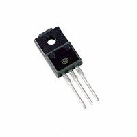
1:Base 2:Collector 3:Emitter TO–220 Full Pack Package(a)
3
Internal Connection
C B
E
s Electrical Characteristics
Parameter Collector cutoff current Emitter cutoff current Collector to emitter voltage Forward current transfer ratio Collector to emitter saturation voltage Base to emitter saturation voltage Transition frequency Turn-on time Storage time Fall time
*V CEO(sus)
(TC=25˚C)
Symbol ICBO ICEO IEBO VCEO(sus)* hFE1 hFE2 VCE(sat) VBE(sat) fT ton tstg tf Conditions VCB = 500V, IE = 0 VCE = 400V, IB = 0 VEB = 12V, IC = 0 IC = 100mA, RBZ = ∞, L = 25mH VCE = 2V, IC = 2A VCE = 2V, IC = 6A IC = 7A, IB = 70mA IC = 7A, IB = 70mA VCE = 10V, IC = 0.5A, f = 1MHz IC = 7A, IB1 = 70mA, IB2 = –70mA, VCC = 300V
X L 25mH Y 15V G 80
min
typ
max 0.1 0.1 100
Unit mA mA mA mA
400 500 200 2.0 2.5 20 1.5 5.0 6.5
V V MHz µs µs µs
Test circuit
60Hz
IC(A) 0.2 0.1 VCE(V)
120Ω 6V 1Ω
1
�Power Transistors
PC — Ta
100 10 (1) TC=Ta (2) With a 100 × 100 × 2mm Al heat sink (3) With a 50 × 50 × 2mm Al heat sink (4) Without heat sink (PC=2.0W) (1) 40 TC=25˚C
2SD1535
IC — VCE
Collector to emitter saturation voltage VCE(sat) (V)
100 IC/IB=100 30 10 TC=100˚C 3 1 –25˚C 0.3 0.1 0.03 0.01 0.01 0.03 25˚C
VCE(sat) — IC
Collector power dissipation PC (W)
Collector current IC (A)
80
8
IB=20mA 10mA
60
6 5mA 4 3mA
20 (2) 0 0 25 50 75 100 125 150 (3) (4)
2
2mA 1mA
0 0 1 2 3 4 5 6
0.1
0.3
1
3
10
Ambient temperature Ta (˚C)
Collector to emitter voltage VCE (V)
Collector current IC (A)
VBE(sat) — IC
100 100000 IC/IB=100
hFE — IC
100 VCE=2V 30
ton, tstg, tf — IC
Pulsed tw=1ms Duty cycle=1% IC/IB=100 (IB1=–IB2) VCC=300V TC=25˚C
Base to emitter saturation voltage VBE(sat) (V)
Forward current transfer ratio hFE
30 10 3 TC=–25˚C 1 100˚C 0.3 0.1 0.03 0.01 0.01 0.03 25˚C
30000
tstg
10000
Switching time ton,tstg,tf (µs)
10 3 1 ton 0.3 0.1 0.03 0.01
3000 1000 300 100 30 10 0.01 0.03
tf
TC=100˚C 25˚C –25˚C
0.1
0.3
1
3
10
0.1
0.3
1
3
10
0
1
2
3
4
5
6
7
8
Collector current IC (A)
Collector current IC (A)
Collector current IC (A)
Area of safe operation (ASO)
100 30 ICP 102 Non repetitive pulse TC=25˚C
Rth(t) — t
(1) Without heat sink (2) With a 100 × 100 × 2mm Al heat sink (1)
10 IC 3 DC 1 0.3 0.1 0.03 0.01 1 3 10 30 1ms
t=0.1ms
Thermal resistance Rth(t) (˚C/W)
Collector current IC (A)
10
(2)
1
10–1
100
300
1000
10–2 10–3
10–2
10–1
1
10
102
103
104
Collector to emitter voltage VCE
(V)
Time t (s)
2
�
很抱歉,暂时无法提供与“2SD1535”相匹配的价格&库存,您可以联系我们找货
免费人工找货