Power F-MOS FETs
2SK3044
Silicon N-Channel Power F-MOS FET
s Features
q Avalanche energy capacity guaranteed: EAS > 130mJ q VGSS = ±30V guaranteed q High-speed switching: tf = 50ns q No secondary breakdown
unit: mm
9.9±0.3 4.6±0.2 2.9±0.2
s Applications
q Contactless relay q Diving circuit for a solenoid q Driving circuit for a motor q Control equipment q Switching power supply
15.0±0.5
φ3.2±0.1
13.7±0.2 4.2±0.2
1.4±0.2 1.6±0.2 0.8±0.1
3.0±0.5
2.6±0.1
0.55±0.15
s Absolute Maximum Ratings (TC = 25°C)
Parameter Drain to Source breakdown voltage Gate to Source voltage Drain current DC Pulse Symbol VDSS VGSS ID IDP EAS* PD Tch Tstg Ratings 450 ±30 ±7 ±14 100 40 2 150 −55 to +150 Unit V V A A mJ W °C °C
1 2
2.54±0.3 3 5.08±0.5
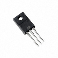
1: Gate 2: Drain 3: Source TO-220D Package
Avalanche energy capacity Allowable power dissipation Channel temperature Storage temperature
*
TC = 25°C Ta = 25°C
L = 4.1mH, IL = 8A, VDD = 50V, 1 pulse
s Electrical Characteristics (TC = 25°C)
Parameter Drain to Source cut-off current Gate to Source leakage current Drain to Source breakdown voltage Gate threshold voltage Drain to Source ON-resistance Forward transfer admittance Diode forward voltage Symbol IDSS IGSS VDSS Vth RDS(on) | Yfs | VDSF Coss td(on) tr td(off) tf VGS = 10V, ID = 4A VDD = 150V, RL = 37.5Ω Conditions VDS = 360V, VGS = 0 VGS = ±30V, VDS = 0 ID = 1mA, VGS = 0 VDS = 25V, ID = 1mA VGS = 10V, ID = 4A VDS = 25V, ID = 4A IDR = 8A, VGS = 0 1300 VDS = 20V, VGS = 0, f = 1MHz 160 70 25 45 150 50 3 450 2 0.56 5 −1.7 5 0.75 min typ max 0.1 ±1 Unit mA µA V V Ω S V pF pF pF ns ns ns ns
Input capacitance (Common Source) Ciss Output capacitance (Common Source) Reverse transfer capacitance (Common Source) Crss Turn-on time (delay time) Rise time Turn-off time (delay time) Fall time
1
�Power F-MOS FETs
Area of safe operation (ASO)
100 30 10 3 1 0.3 10ms 0.1 100ms 0.03 0.01 1 3 10 30 100 300 1000 DC 100µs 1ms 60
2SK3044
PD Ta
100
EAS Tj
Avalanche energy capacity EAS (mJ)
Allowable power dissipation PD (W)
Non repetitive pulse TC=25˚C t=10µs
(1) TC=Ta (2) Without heat sink 50
80
Drain current ID (A)
40 (1) 30
60
40
20
10 (2) 0 0 20 40 60 80 100 120 140 160
20
0 25
50
75
100
125
150
175
Drain to source voltage VDS (V)
Ambient temperature Ta (˚C)
Junction temperature Tj (˚C)
ID VDS
16 14 12 10 8 6V 6 4 2 0 0 10 20 30 40 50 60 5.5V VGS=15V 10V 8 TC=25˚C 10
ID VGS
6 VDS=25V 25˚C 100˚C
Vth TC
VDS=25V ID=1mA 5
Drain current ID (A)
Drain current ID (A)
7V
TC=0˚C
150˚C
Gate threshold voltage Vth (V)
10 12
4
6
3
4
2
2 5V 50W 0 0 2 4 6 8
1
0 0 25 50 75 100 125 150
Drain to source voltage VDS (V)
Gate to source voltage VGS (V)
Case temperature TC (˚C)
RDS(on) ID
Drain to source ON-resistance RDS(on) (Ω)
VGS=10V 2.0
RDS(on) ID
Drain to source ON-resistance RDS(on) (Ω)
2.4 12
| Yfs | ID
Forward transfer admittance |Yfs| (S)
TC=25˚C VDS=25V TC=25˚C 10
2.4
2.0
1.6 TC=150˚C 100˚C 0.8 25˚C 0.4 0˚C
1.6
8
1.2
1.2
6
0.8 VGS=10V 0.4 15V
4
2
0 0 2 4 6 8 10
0 0 2 4 6 8 10
0 0 2 4 6 8 10
Drain current ID (A)
Drain current ID (A)
Drain current ID (A)
2
�Power F-MOS FETs
Ciss, Coss, Crss VDS
Input capacitance (Common source), Output capacitance (Common source), Reverse transfer capacitance (Common source) Ciss,Coss,Crss (pF)
10000 3000 1000 300 100 Coss 30 10 3 1 0 50 100 150 200 250 Crss f=1MHz TC=25˚C
2SK3044
VDS, VGS Qg
400 16 14 12 10 8 6 4 VGS 50 0 0 10 20 30 40 50 2 0 60 300 ID=8A TC=25˚C
td(on), tr, tf, td(off) ID
VDD=150V VGS=10V TC=25˚C
Drain to source voltage VDS (V)
Gate to source voltage VGS (V)
350 300 250 200 150 100
Switching time td(on),tr,tf,td(off) (ns)
250
Ciss
200
VDS
150 td(off) 100 tf 50 tr td(on) 0 0 2 4 6 8 10
Drain to source voltage VDS (V)
Gate charge amount Qg (nC)
Drain current ID (A)
Rth(t) t
102 (1) Without heat sink (2) With a 100 × 100 × 2mm Al heat sink (1)
Thermal resistance Rth(t) (˚C/W)
10
(2)
1
10–1
10–2 10–4
10–3
10–2
10–1
1
10
102
103
104
Time t (s)
3
�
很抱歉,暂时无法提供与“2SK3044”相匹配的价格&库存,您可以联系我们找货
免费人工找货