Power MOSFETs
2SK3318
Silicon N-channel power MOSFET
(0.7)
Unit: mm
15.0±0.3 11.0±0.2 5.0±0.2 (3.2)
For switching ■ Features
• Avalanche energy capability guaranteed • High-speed switching • Low ON resistance Ron • No secondary breakdown
21.0±0.5
φ 3.2±0.1
(3.5) Solder Dip
15.0±0.2
2.0±0.2 1.1±0.1
2.0±0.1 0.6±0.2
■ Absolute Maximum Ratings TC = 25°C
Parameter Drain-source surrender voltage Gate-source surrender voltage Drain current Peak drain current Avalanche energy capability * Power dissipation T a = 25 ° C Tch Tstg Symbol VDSS VGSS ID IDP EAS PD Rating 600 ±30 ±15 ±60 112.5 100 3 150 −55 to +150 °C °C Unit V V A A mJ W
16.2±0.5
5.45±0.3 10.9±0.5 1 2 3
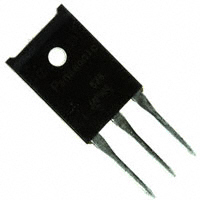
1: Gate 2: Drain 3: Source TOP-3F-A1 Package
Internal Connection
D G S
Conditions Min 600 −1.5 2 4 10 ±1 0.33 6 10 3 500 340 50 0.46 Typ Max Unit V V V µA µA Ω S pF pF pF ns ns ns ns 1.25 41.7 °C/W °C/W
Channel temperature Storage temperature Note) *: L = 1 mH, IL = 15 A, 1 pulse
■ Electrical Characteristics TC = 25°C ± 3°C
Parameter Gate-drain surrender voltage Diode forward voltage Gate threshold voltage Drain-source cutoff current Gate-source cutoff currentt Drain-source on resistance Forward transfer admittance Short-circuit forward transfer capacitance (Common-source) Short-circuit output capacitance (Common-source) Reverse transfer capacitance (Common-source) Turn-on delay time Rise time Turn-off delay time Fall time Channel-case heat resistance Channel-atmosphere heat resistance Symbol VDSS VDSF Vth IDSS IGSS RDS(on) Yfs Ciss Coss Crss td(on) tr td(off) tf Rth(ch-c) Rth(ch-a) VDD = 150 V, ID = 7.5 A RL = 20 Ω, VGS = 10 V ID = 1 mA, VGS = 0 IDR = 15 A, VGS = 0 VDS = 25 V, ID = 1 mA VDS = 480 V, VGS = 0 VGS = ±30 V, VDS = 0 VGS = 10 V, ID = 7.5 A VDS = 25 V, ID = 7.5 A VDS = 20 V, VGS = 0, f = 1 MHz
40 55 310 70
Note) Measuring methods are based on JAPANESE INDUSTRIAL STANDARD JIS C 7030 measuring methods for transistors.
Publication date: November 2004 SJG00040AED
1
�2SK3318
Safe operation area
103 Non repetitive pulse TC = 25°C
120 (1)
PD Ta
(1) TC = Ta (2) Without heat sink PD = 3 W
100
Drain current ID (A)
102 I DP
t = 100 µs
Power dissipation PD (W)
103
80
ID 10 RDS(on) Limited 1 ms 1 10 ms 100 ms DC 10−1
60
40
20 (2)
1
10
102
0
0
50
100
150
Drain-source voltage VDS (V)
Ambient temperature Ta (°C)
2
SJG00040AED
�Request for your special attention and precautions in using the technical information and semiconductors described in this material
(1) An export permit needs to be obtained from the competent authorities of the Japanese Government if any of the products or technical information described in this material and controlled under the "Foreign Exchange and Foreign Trade Law" is to be exported or taken out of Japan. (2) The technical information described in this material is limited to showing representative characteristics and applied circuits examples of the products. It neither warrants non-infringement of intellectual property right or any other rights owned by our company or a third party, nor grants any license. (3) We are not liable for the infringement of rights owned by a third party arising out of the use of the technical information as described in this material. (4) The products described in this material are intended to be used for standard applications or general electronic equipment (such as office equipment, communications equipment, measuring instruments and household appliances). Consult our sales staff in advance for information on the following applications: • Special applications (such as for airplanes, aerospace, automobiles, traffic control equipment, combustion equipment, life support systems and safety devices) in which exceptional quality and reliability are required, or if the failure or malfunction of the products may directly jeopardize life or harm the human body. • Any applications other than the standard applications intended. (5) The products and product specifications described in this material are subject to change without notice for modification and/or improvement. At the final stage of your design, purchasing, or use of the products, therefore, ask for the most up-to-date Product Standards in advance to make sure that the latest specifications satisfy your requirements. (6) When designing your equipment, comply with the guaranteed values, in particular those of maximum rating, the range of operating power supply voltage, and heat radiation characteristics. Otherwise, we will not be liable for any defect which may arise later in your equipment. Even when the products are used within the guaranteed values, take into the consideration of incidence of break down and failure mode, possible to occur to semiconductor products. Measures on the systems such as redundant design, arresting the spread of fire or preventing glitch are recommended in order to prevent physical injury, fire, social damages, for example, by using the products. (7) When using products for which damp-proof packing is required, observe the conditions (including shelf life and amount of time let standing of unsealed items) agreed upon when specification sheets are individually exchanged. (8) This material may be not reprinted or reproduced whether wholly or partially, without the prior written permission of Matsushita Electric Industrial Co., Ltd.
2003 SEP
�
很抱歉,暂时无法提供与“2SK3318”相匹配的价格&库存,您可以联系我们找货
免费人工找货