Voltage Regulators
AN80LXXRMS Series
Low-drop type positive output voltage regulator IC
s Overview
The AN80LXXRMS series is 0.15 A output low-drop output type positive voltage regulator IC with resetting function. 20 classifications of output voltages, 1.8 V, 1.9 V, 2.0 V, 2.1 V, 2.2 V, 2.5 V, 2.8 V, 2.9 V, 3.0 V, 3.1 V, 3.2 V, 3.3 V, 3.4 V, 3.5 V, 3.6 V, 4.8 V, 4.9 V, 5.0 V, 5.1 V and 5.2 V are available. In addition, it is adopting the surface mounting type package (Mini 5-pin plastic package), so that it is most suited for miniaturization and weight reduction of set equipment.
0.65±0.15 5
1.9±0.1 0.95 0.95
2.9 –0.05
2.8 –0.3
+0.2
Unit : mm
0.65±0.15
1.45±0.1
+0.1 0.16 –0.06
+0.25 1.5 –0.05
1
+0.2
4
3
2
0.3 –0.05
+0.1
• Minimum input and output voltage difference : 0.4 V max. • High precision output voltage : (allowance : ± 3%) • Built-in reset function terminal (High : Active) • Built-in overcurrent limiting circuit • Built-in circuit for limiting rush current at input voltage rising time • Output voltage : 1.8 V to 5.2 V
0.8
s Features
1.1 –0.1
+0.2
0 to 0.1
0.1 to 0.3 0.4±0.2
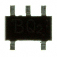
Mini-type 5-pin Type name indication symbol : XX
s Applications
• Cellular phone, PHS, analog cordless phone, other small sized potable equipment
s Block diagram
IN 1
2
OUT
Current source
CONT 5
Start / Stop Bandgap reference
Error amp. 3 N.C.
GND 4
1
�AN80LXXRMS Series
s Output Voltage Characteristics at IOUT = 50 mA, Ta = 25°C
Type No. AN80L18RMS AN80L19RMS AN80L20RMS AN80L21RMS AN80L22RMS AN80L25RMS AN80L28RMS AN80L29RMS AN80L30RMS AN80L31RMS AN80L32RMS AN80L33RMS AN80L34RMS AN80L35RMS AN80L36RMS AN80L48RMS AN80L49RMS AN80L50RMS AN80L51RMS AN80L52RMS Output V 1.8 1.9 2.0 2.1 2.2 2.5 2.8 2.9 3.0 3.1 3.2 3.3 3.4 3.5 3.6 4.8 4.9 5.0 5.1 5.2 Conditions VIN = 2.8 V 2.9 3.0 3.1 3.2 3.5 3.8 3.9 4.0 4.1 4.2 4.3 4.4 4.5 4.6 5.8 5.9 6.0 6.1 6.2 min. 1.746 1.843 1.940 2.037 2.134 2.452 2.716 2.813 2.910 3.007 3.104 3.201 3.298 3.395 3.492 4.656 4.753 4.850 4.947 5.044 typ. 1.8 1.9 2.0 2.1 2.2 2.5 2.8 2.9 3.0 3.1 3.2 3.3 3.4 3.5 3.6 4.8 4.9 5.0 5.1 5.2
Voltage Regulators
max. 1.854 1.957 2.060 2.163 2.266 2.575 2.884 2.987 3.090 3.193 3.296 3.399 3.502 3.605 3.708 4.944 5.047 5.150 5.253 5.356
Unit V
Marking BA BB BC BD BE BW BF BG BH BJ BK BL BM BN BP BQ BR BS BT BU
BA
(Marking example : AN80L18RMS)
2
�Voltage Regulators Common to the AN80LXXRMS Series
s Pin Descriptions
Pin No. 1 2 3 4 5 Description Input voltage pin Output voltage pin N.C. pin Grounding pin Control pin ("High" → operation "Low" → stop)
AN80LXXRMS Series
s Absolute Maximum Ratings
Parameter Supply voltage *1 Supply current Power dissipation *3 Operating ambient temperature *2 Storage temperature *2 Symbol VCC ICC PD Topr Tstg Rating 14.6 300 78 −30 to +85 −55 to +150 Unit V mA mW °C °C
Note) *1 : There may be a case of the device destruction when the output (VOUT) and the grounding (GND), or the output (VOUT) and input (VIN) are short-circuited. 2 : All items are at Ta = 25°C, except for the parameter of operating ambient temperature and storage temperature. * *3 : Topr = Power dissipation for IC alone without heat sink at + 85°C.
3
�AN80LXXRMS Series AN80L18RMS (1.8 V)
s Recommended Operating Range
Parameter Supply voltage Symbol VCC Range 2.2 to 14.5
Voltage Regulators
Unit V
s Electrical Characteristics at Ta = 25°C
Note) Unless otherwise specially provided, shorten each test time (within 10 ms) so that the test is conducted under the condition that the drift due to the temperature increase in the chip junction part can be neglected. CIN = 0.1 µF, COUT = 10 µF
Parameter Output voltage Input stability 1 Input stability 2 Load stability
*1 *2
Symbol VOUT REGIN1 REGIN2 REGLOA IPEAK
Conditions VIN = 2.8 V, IOUT = 50 mA VIN = 2.8 V → 14.5 V, IOUT = 50 mA VIN = 2.8 V → 9 V, IOUT = 50 mA VIN = 2.8 V, IOUT = 0 mA → 150 mA VIN = 2.8 V, The output current value decreases by 5% from the value when VOUT is at IOUT = 50 mA. VIN = 2.8 V, IOUT = 0 mA VIN = 2.8 V, IOUT = 0 mA → 150 mA VIN = 10 V, VCONT = 0 V VIN = 1.5 V, IOUT = 0 mA 1 Vrms, f = 120 Hz, IOUT = 10 mA VIN = 1.5 V, IOUT = 0 mA VIN = 2.1 V, IOUT = 150 mA VIN = 2.8 V, IOUT = 50 mA VIN = 2.8 V, IOUT = 50 mA VIN = 2.8 V, IOUT = 50 mA VCONT = 1.8 V
Min 1.746 180
Typ 1.8 10 5 50 240
Max 1.854 50 20 150
Unit V mV mV mV mA
Peak output current
Bias current without load
IBIAS
62 0.30
1.5 70 0.1
350 5 0.1 5 0.2 0.4 1.50 30
µA mA µA mA dB V V V V µA
Bias current fluctuation with load ∆IBIAS Standby consumption current Bias current before starting regulation Ripple rejection ratio Minimum input and output voltage difference 1 Minimum input and output voltage difference 2 ISTB IRUSH R.R. VDIF(min)1 VDIF(min)2
Control terminal threshold high voltage VCONTH Control terminal threshold low voltage Control terminal current VCONTL ICONT
Note) *1 : 1.0 Ω *2 : Peak output current : The output current when the output voltage has been decreased by 5% from the value at the time of the output current is 50 mA due to the overcurrent protection.
• Design reference data
Note) The following values are typical and not guaranteed values.
Parameter Output noise voltage Output voltage temperature coefficient Output rise time
Symbol VNO 1 dVOUT ・ VOUT dT tON
Conditions 10Hz ≤ f ≤ 100kHz, IOUT = 10 mA VIN = 2.8 V, IOUT = 0 mA − 30°C ≤ Ta ≤ + 85°C VIN = 2.8 V, IOUT = 50 mA VCONT = 0 V → 1.8 V, CIN = 0.1 µF COUT = 10 µF, VOUT = 90%
Min
Typ 38 90 0.10
Max
Unit µV ppm/°C ms
Note) *1 : Refer to s Technical Information " • Output rise time characteristics".
4
�Voltage Regulators AN80L19RMS (1.9 V)
s Recommended Operating Range
Parameter Supply voltage Symbol VCC Range 2.3 to 14.5
AN80LXXRMS Series
Unit V
s Electrical Characteristics at Ta = 25°C
Note) Unless otherwise specially provided, shorten each test time (within 10 ms) so that the test is conducted under the condition that the drift due to the temperature increase in the chip junction part can be neglected. CIN = 0.1 µF, COUT = 10 µF
Parameter Output voltage Input stability 1 Input stability 2 Load stability
*1 *2
Symbol VOUT REGIN1 REGIN2 REGLOA IPEAK
Conditions VIN = 2.9 V, IOUT = 50 mA VIN = 2.9 V → 14.5 V, IOUT = 50 mA VIN = 2.9 V → 9 V, IOUT = 50 mA VIN = 2.9 V, IOUT = 0 mA → 150 mA VIN = 2.9 V, The output current value decreases by 5% from the value when VOUT is at IOUT = 50 mA. VIN = 2.9 V, IOUT = 0 mA VIN = 2.9 V, IOUT = 0 mA → 150 mA VIN = 10 V, VCONT = 0 V VIN = 1.6 V, IOUT = 0 mA 1 Vrms, f = 120 Hz, IOUT = 10 mA VIN = 1.6 V, IOUT = 0 mA VIN = 2.2 V, IOUT = 150 mA VIN = 2.9 V, IOUT = 50 mA VIN = 2.9 V, IOUT = 50 mA VIN = 2.9 V, IOUT = 50 mA VCONT = 1.8 V
Min 1.843 180
Typ 1.9 10 5 50 240
Max 1.957 50 20 150
Unit V mV mV mV mA
Peak output current
Bias current without load
IBIAS
62 0.30
1.5 70 0.1
350 5 0.1 5 0.2 0.4 1.50 30
µA mA µA mA dB V V V V µA
Bias current fluctuation with load ∆IBIAS Standby consumption current Bias current before starting regulation Ripple rejection ratio Minimum input and output voltage difference 1 Minimum input and output voltage difference 2 ISTB IRUSH R.R. VDIF(min)1 VDIF(min)2
Control terminal threshold high voltage VCONTH Control terminal threshold high voltage VCONTH Control terminal current ICONT
Note) *1 : 1.0 Ω *2 : Peak output current : The output current when the output voltage has been decreased by 5% from the value at the time of the output current is 50 mA due to the overcurrent protection.
• Design reference data
Note) The following values are typical and not guaranteed values.
Parameter Output noise voltage Output voltage temperature coefficient Output rise time
Symbol VNO 1 dVOUT ・ VOUT dT tON
Conditions 10Hz ≤ f ≤ 100kHz, IOUT = 10 mA VIN = 2.9 V, IOUT = 0 mA − 30°C ≤ Ta ≤ + 85°C VIN = 2.9 V, IOUT = 50 mA VCONT = 0 V → 1.8 V, CIN = 0.1 µF COUT = 10 µF, VOUT = 90%
Min
Typ 40 90 0.10
Max
Unit µV ppm/°C ms
Note) *1 : Refer to s Technical Information " • Output rise time characteristics".
5
�AN80LXXRMS Series AN80L20RMS (2.0 V)
s Recommended Operating Range
Parameter Supply voltage Symbol VCC Range 2.4 to 14.5
Voltage Regulators
Unit V
s Electrical Characteristics at Ta = 25°C
Note) Unless otherwise specially provided, shorten each test time (within 10 ms) so that the test is conducted under the condition that the drift due to the temperature increase in the chip junction part can be neglected. CIN = 0.1 µF, COUT = 10 µF
Parameter Output voltage Input stability 1 Input stability 2 Load stability
*1 *2
Symbol VOUT REGIN1 REGIN2 REGLOA IPEAK
Conditions VIN = 3.0 V, IOUT = 50 mA VIN = 3.0 V → 14.5 V, IOUT = 50 mA VIN = 3.0 V → 9 V, IOUT = 50 mA VIN = 3.0 V, IOUT = 0 mA → 150 mA VIN = 3.0 V, The output current value decreases by 5% from the value when VOUT is at IOUT = 50 mA. VIN = 3.0 V, IOUT = 0 mA VIN = 3.0 V, IOUT = 0 mA → 150 mA VIN = 10 V, VCONT = 0 V VIN = 1.7 V, IOUT = 0 mA 1 Vrms, f = 120 Hz, IOUT = 10 mA VIN = 1.7 V, IOUT = 0 mA VIN = 2.3 V, IOUT = 150 mA VIN = 3.0 V, IOUT = 50 mA VIN = 3.0 V, IOUT = 50 mA VIN = 3.0 V, IOUT = 50 mA VCONT = 1.8 V
Min 1.940 180
Typ 2.0 10 5 50 240
Max 2.060 50 20 150
Unit V mV mV mV mA
Peak output current
Bias current without load
IBIAS
62 0.30
1.5 70 0.1
350 5 0.1 5 0.2 0.4 1.50 30
µA mA µA mA dB V V V V µA
Bias current fluctuation with load ∆IBIAS Standby consumption current Bias current before starting regulation Ripple rejection ratio Minimum input and output voltage difference 1 Minimum input and output voltage difference 2 ISTB IRUSH R.R. VDIF(min)1 VDIF(min)2
Control terminal threshold high voltage VCONTH Control terminal threshold high voltage VCONTH Control terminal current ICONT
Note) *1 : 1.0 Ω *2 : Peak output current : The output current when the output voltage has been decreased by 5% from the value at the time of the output current is 50 mA due to the overcurrent protection.
• Design reference data
Note) The following values are typical and not guaranteed values.
Parameter Output noise voltage Output voltage temperature coefficient Output rise time
Symbol VNO 1 dVOUT ・ VOUT dT tON
Conditions 10Hz ≤ f ≤ 100kHz, IOUT = 10 mA VIN = 3.0 V, IOUT = 0 mA − 30°C ≤ Ta ≤ + 85°C VIN = 3.0 V, IOUT = 50 mA VCONT = 0 V → 1.8 V, CIN = 0.1 µF COUT = 10 µF, VOUT = 90%
Min
Typ 42 90 0.10
Max
Unit µV ppm/°C ms
Note) *1 : Refer to s Technical Information " • Output rise time characteristics".
6
�Voltage Regulators AN80L21RMS (2.1 V)
s Recommended Operating Range
Parameter Supply voltage Symbol VCC Range 2.5 to 14.5
AN80LXXRMS Series
Unit V
s Electrical Characteristics at Ta = 25°C
Note) Unless otherwise specially provided, shorten each test time (within 10 ms) so that the test is conducted under the condition that the drift due to the temperature increase in the chip junction part can be neglected. CIN = 0.1 µF, COUT = 10 µF
Parameter Output voltage Input stability 1 Input stability 2 Load stability
*1 *2
Symbol VOUT REGIN1 REGIN2 REGLOA IPEAK
Conditions VIN = 3.1 V, IOUT = 50 mA VIN = 3.1 V → 14.5 V, IOUT = 50 mA VIN = 3.1 V → 9 V, IOUT = 50 mA VIN = 3.1 V, IOUT = 0 mA → 150 mA VIN = 3.1 V, The output current value decreases by 5% from the value when VOUT is at IOUT = 50 mA. VIN = 3.1 V, IOUT = 0 mA VIN = 3.1 V, IOUT = 0 mA → 150 mA VIN = 10 V, VCONT = 0 V VIN = 1.8 V, IOUT = 0 mA 1 Vrms, f = 120 Hz, IOUT = 10 mA VIN = 1.8 V, IOUT = 0 mA VIN = 2.4 V, IOUT = 150 mA VIN = 3.1 V, IOUT = 50 mA VIN = 3.1 V, IOUT = 50 mA VIN = 3.1 V, IOUT = 50 mA VCONT = 1.8 V
Min 2.037 180
Typ 2.1 10 5 50 240
Max 2.163 50 20 150
Unit V mV mV mV mA
Peak output current
Bias current without load
IBIAS
61 0.30
1.5 69 0.1
350 5 0.1 5 0.2 0.4 1.50 30
µA mA µA mA dB V V V V µA
Bias current fluctuation with load ∆IBIAS Standby consumption current Bias current before starting regulation Ripple rejection ratio Minimum input and output voltage difference 1 Minimum input and output voltage difference 2 ISTB IRUSH R.R. VDIF(min)1 VDIF(min)2
Control terminal threshold high voltage VCONTH Control terminal threshold high voltage VCONTH Control terminal current ICONT
Note) *1 : 1.0 Ω *2 : Peak output current : The output current when the output voltage has been decreased by 5% from the value at the time of the output current is 50 mA due to the overcurrent protection.
• Design reference data
Note) The following values are typical and not guaranteed values.
Parameter Output noise voltage Output voltage temperature coefficient Output rise time
Symbol VNO 1 dVOUT ・ VOUT dT tON
Conditions 10Hz ≤ f ≤ 100kHz, IOUT = 10 mA VIN = 3.1 V, IOUT = 0 mA − 30°C ≤ Ta ≤ + 85°C VIN = 3.1 V, IOUT = 50 mA VCONT = 0 V → 1.8 V, CIN = 0.1 µF COUT = 10 µF, VOUT = 90%
Min
Typ 44 90 0.10
Max
Unit µV ppm/°C ms
Note) *1 : Refer to s Technical Information " • Output rise time characteristics".
7
�AN80LXXRMS Series AN80L22RMS (2.2 V)
s Recommended Operating Range
Parameter Supply voltage Symbol VCC Range 2.6 to 14.5
Voltage Regulators
Unit V
s Electrical Characteristics at Ta = 25°C
Note) Unless otherwise specially provided, shorten each test time (within 10 ms) so that the test is conducted under the condition that the drift due to the temperature increase in the chip junction part can be neglected. CIN = 0.1 µF, COUT = 10 µF
Parameter Output voltage Input stability 1 Input stability 2 Load stability
*1 *2
Symbol VOUT REGIN1 REGIN2 REGLOA IPEAK
Conditions VIN = 3.2 V, IOUT = 50 mA VIN = 3.2 V → 14.5 V, IOUT = 50 mA VIN = 3.2 V → 9 V, IOUT = 50 mA VIN = 3.2 V, IOUT = 0 mA → 150 mA VIN = 3.2 V, The output current value decreases by 5% from the value when VOUT is at IOUT = 50 mA. VIN = 3.2 V, IOUT = 0 mA VIN = 3.2 V, IOUT = 0 mA → 150 mA VIN = 10 V, VCONT = 0 V VIN = 1.9 V, IOUT = 0 mA 1 Vrms, f = 120 Hz, IOUT = 10 mA VIN = 1.9 V, IOUT = 0 mA VIN = 2.4 V, IOUT = 150 mA VIN = 3.2 V, IOUT = 50 mA VIN = 3.2 V, IOUT = 50 mA VIN = 3.2 V, IOUT = 50 mA VCONT = 1.8 V
Min 2.134 180
Typ 2.2 10 5 50 240
Max 2.266 50 20 150
Unit V mV mV mV mA
Peak output current
Bias current without load
IBIAS
61 0.30
1.5 69 0.1
350 5 0.1 5 0.2 0.4 1.50 30
µA mA µA mA dB V V V V µA
Bias current fluctuation with load ∆IBIAS Standby consumption current Bias current before starting regulation Ripple rejection ratio Minimum input and output voltage difference 1 Minimum input and output voltage difference 2 ISTB IRUSH R.R. VDIF(min)1 VDIF(min)2
Control terminal threshold high voltage VCONTH Control terminal threshold high voltage VCONTH Control terminal current ICONT
Note) *1 : 1.0 Ω *2 : Peak output current : The output current when the output voltage has been decreased by 5% from the value at the time of the output current is 50 mA due to the overcurrent protection.
• Design reference data
Note) The following values are typical and not guaranteed values.
Parameter Output noise voltage Output voltage temperature coefficient Output rise time
Symbol VNO 1 dVOUT ・ VOUT dT tON
Conditions 10Hz ≤ f ≤ 100kHz, IOUT =10 mA VIN = 3.2 V, IOUT = 0 mA − 30°C ≤ Ta ≤ + 85°C VIN = 3.2 V, IOUT = 50 mA VCONT = 0 V → 1.8 V, CIN = 0.1 µF COUT = 10 µF, VOUT = 90%
Min
Typ 46 90 0.10
Max
Unit µV ppm/°C ms
Note) *1 : Refer to s Technical Information " • Output rise time characteristics".
8
�Voltage Regulators AN80L25RMS (2.5 V)
s Recommended Operating Range
Parameter Supply voltage Symbol VCC Range 2.9 to 14.5
AN80LXXRMS Series
Unit V
s Electrical Characteristics at Ta = 25°C
Note) Unless otherwise specially provided, shorten each test time (within 10 ms) so that the test is conducted under the condition that the drift due to the temperature increase in the chip junction part can be neglected. CIN = 0.1 µF, COUT = 10 µF
Parameter Output voltage Input stability 1 Input stability 2 Load stability
*1 *2
Symbol VOUT REGIN1 REGIN2 REGLOA IPEAK
Conditions VIN = 3.5 V, IOUT = 50 mA VIN = 3.5 V → 14.5 V, IOUT = 50 mA VIN = 3.5 V → 9 V, IOUT = 50 mA VIN = 3.5 V, IOUT = 0 mA → 150 mA VIN = 3.5 V, The output current value decreases by 5% from the value when VOUT is at IOUT = 50 mA. VIN = 3.5 V, IOUT = 0 mA VIN = 3.5 V, IOUT = 0 mA → 150 mA VIN = 10 V, VCONT = 0 V VIN = 2.2 V, IOUT = 0 mA 1 Vrms, f = 120 Hz, IOUT = 10 mA VIN = 2.2 V, IOUT = 0 mA VIN = 2.6 V, IOUT = 150 mA VIN = 3.5 V, IOUT = 50 mA VIN = 3.5 V, IOUT = 50 mA VIN = 3.5 V, IOUT = 50 mA VCONT = 1.8 V
Min 2.425 180
Typ 2.5 10 5 50 240
Max 2.575 50 20 150
Unit V mV mV mV mA
Peak output current
Bias current without load
IBIAS
60 0.30
1.5 68 0.1
350 5 0.1 5 0.2 0.4 1.50 30
µA mA µA mA dB V V V V µA
Bias current fluctuation with load ∆IBIAS Standby consumption current Bias current before starting regulation Ripple rejection ratio Minimum input and output voltage difference 1 Minimum input and output voltage difference 2 ISTB IRUSH R.R. VDIF(min)1 VDIF(min)2
Control terminal threshold high voltage VCONTH Control terminal threshold high voltage VCONTH Control terminal current ICONT
Note) *1 : 1.0 Ω *2 : Peak output current : The output current when the output voltage has been decreased by 5% from the value at the time of the output current is 50 mA due to the overcurrent protection.
• Design reference data
Note) The following values are typical and not guaranteed values.
Parameter Output noise voltage Output voltage temperature coefficient Output rise time
Symbol VNO 1 dVOUT ・ VOUT dT tON
Conditions 10Hz ≤ f ≤ 100kHz, IOUT = 10 mA VIN = 3.5 V, IOUT = 0 mA − 30°C ≤ Ta ≤ + 85°C VIN = 3.15 V, IOUT = 50 mA VCONT = 0 V → 1.8 V, CIN = 0.1 µF COUT = 10 µF, VOUT = 90%
Min
Typ 58 90 0.10
Max
Unit µV ppm/°C ms
Note) *1 : Refer to s Technical Information " • Output rise time characteristics".
9
�AN80LXXRMS Series AN80L28RMS (2.8 V)
s Recommended Operating Range
Parameter Supply voltage Symbol VCC Range 3.2 to 14.5
Voltage Regulators
Unit V
s Electrical Characteristics at Ta = 25°C
Note) Unless otherwise specially provided, shorten each test time (within 10 ms) so that the test is conducted under the condition that the drift due to the temperature increase in the chip junction part can be neglected. CIN = 0.1 µF, COUT = 10 µF
Parameter Output voltage Input stability 1 Input stability 2 Load stability
*1 *2
Symbol VOUT REGIN1 REGIN2 REGLOA IPEAK
Conditions VIN = 3.8 V, IOUT = 50 mA VIN = 3.8 V → 14.5 V, IOUT = 50 mA VIN = 3.8 V → 9 V, IOUT = 50 mA VIN = 3.8 V, IOUT = 0 mA → 150 mA VIN = 3.8 V, The output current value decreases by 5% from the value when VOUT is at IOUT = 50 mA. VIN = 3.8 V, IOUT = 0 mA VIN = 3.8 V, IOUT = 0 mA → 150 mA VIN = 10 V, VCONT = 0 V VIN = 2.5 V, IOUT = 0 mA 1 Vrms, f = 120 Hz, IOUT = 10 mA VIN = 2.5 V, IOUT = 0 mA VIN = 2.9 V, IOUT = 150 mA VIN = 3.8 V, IOUT = 50 mA VIN = 3.8 V, IOUT = 50 mA VIN = 3.8 V, IOUT = 50 mA VCONT = 1.8 V
Min 2.716 180
Typ 2.8 10 5 50 240
Max 2.884 50 20 150
Unit V mV mV mV mA
Peak output current
Bias current without load
IBIAS
60 0.30
1.5 68 0.1
350 5 0.1 5 0.2 0.4 1.50 30
µA mA µA mA dB V V V V µA
Bias current fluctuation with load ∆IBIAS Standby consumption current Bias current before starting regulation Ripple rejection ratio Minimum input and output voltage difference 1 Minimum input and output voltage difference 2 ISTB IRUSH R.R. VDIF(min)1 VDIF(min)2
Control terminal threshold high voltage VCONTH Control terminal threshold high voltage VCONTH Control terminal current ICONT
Note) *1 : 1.0 Ω *2 : Peak output current : The output current when the output voltage has been decreased by 5% from the value at the time of the output current is 50 mA due to the overcurrent protection.
• Design reference data
Note) The following values are typical and not guaranteed values.
Parameter Output noise voltage Output voltage temperature coefficient Output rise time
Symbol VNO 1 dVOUT ・ VOUT dT tON
Conditions 10Hz ≤ f ≤ 100kHz, IOUT =10 mA VIN = 3.8 V, IOUT = 0 mA − 30°C ≤ Ta ≤ + 85°C VIN = 3.8 V, IOUT = 50 mA VCONT = 0 V → 1.8 V, CIN = 0.1 µF COUT = 10 µF, VOUT = 90%
Min
Typ 58 90 0.10
Max
Unit µV ppm/°C ms
Note) *1 : Refer to s Technical Information " • Output rise time characteristics".
10
�Voltage Regulators AN80L29RMS (2.9 V)
s Recommended Operating Range
Parameter Supply voltage Symbol VCC Range 3.3 to 14.5
AN80LXXRMS Series
Unit V
s Electrical Characteristics at Ta = 25°C
Note) Unless otherwise specially provided, shorten each test time (within 10 ms) so that the test is conducted under the condition that the drift due to the temperature increase in the chip junction part can be neglected. CIN = 0.1 µF, COUT = 10 µF
Parameter Output voltage Input stability 1 Input stability 2 Load stability
*1 *2
Symbol VOUT REGIN1 REGIN2 REGLOA IPEAK
Conditions VIN = 3.9 V, IOUT = 50 mA VIN = 3.9 V → 14.5 V, IOUT = 50 mA VIN = 3.9 V → 9 V, IOUT = 50 mA VIN = 3.9 V, IOUT = 0 mA → 150 mA VIN = 3.9 V, The output current value decreases by 5% from the value when VOUT is at IOUT = 50 mA. VIN = 3.9 V, IOUT = 0 mA VIN = 3.9 V, IOUT = 0 mA → 150 mA VIN = 10 V, VCONT = 0 V VIN = 2.6 V, IOUT = 0 mA 1 Vrms, f = 120 Hz, IOUT = 10 mA VIN = 2.6 V, IOUT = 0 mA VIN = 3.0 V, IOUT = 150 mA VIN = 3.9 V, IOUT = 50 mA VIN = 3.9 V, IOUT = 50 mA VIN = 3.9 V, IOUT = 50 mA VCONT = 1.8 V
Min 2.813 180
Typ 2.9 10 5 50 240
Max 2.987 50 20 150
Unit V mV mV mV mA
Peak output current
Bias current without load
IBIAS
60 0.30
1.5 68 0.1
350 5 0.1 5 0.2 0.4 1.50 30
µA mA µA mA dB V V V V µA
Bias current fluctuation with load ∆IBIAS Standby consumption current Bias current before starting regulation Ripple rejection ratio Minimum input and output voltage difference 1 Minimum input and output voltage difference 2 ISTB IRUSH R.R. VDIF(min)1 VDIF(min)2
Control terminal threshold high voltage VCONTH Control terminal threshold high voltage VCONTH Control terminal current ICONT
Note) *1 : 1.0 Ω *2 : Peak output current : The output current when the output voltage has been decreased by 5% from the value at the time of the output current is 50 mA due to the overcurrent protection.
• Design reference data
Note) The following values are typical and not guaranteed values.
Parameter Output noise voltage Output voltage temperature coefficient Output rise time
Symbol VNO 1 dVOUT ・ VOUT dT tON
Conditions 10Hz ≤ f ≤ 100kHz, IOUT = 10 mA VIN = 3.9 V, IOUT = 0 mA − 30°C ≤ Ta ≤ + 85°C VIN = 3.9 V, IOUT = 50 mA VCONT = 0 V → 1.8 V, CIN = 0.1 µF COUT = 10 µF, VOUT = 90%
Min
Typ 60 90 0.12
Max
Unit µV ppm/°C ms
Note) *1 : Refer to s Technical Information " • Output rise time characteristics".
11
�AN80LXXRMS Series AN80L30RMS (3.0 V)
s Recommended Operating Range
Parameter Supply voltage Symbol VCC Range 3.4 to 14.5
Voltage Regulators
Unit V
s Electrical Characteristics at Ta = 25°C
Note) Unless otherwise specially provided, shorten each test time (within 10 ms) so that the test is conducted under the condition that the drift due to the temperature increase in the chip junction part can be neglected. CIN = 0.1 µF, COUT = 10 µF
Parameter Output voltage Input stability 1 Input stability 2 Load stability
*1 *2
Symbol VOUT REGIN1 REGIN2 REGLOA IPEAK
Conditions VIN = 4.0 V, IOUT = 50 mA VIN = 4.0 V → 14.5 V, IOUT = 50 mA VIN = 4.0 V → 9 V, IOUT = 50 mA VIN = 4.0 V, IOUT = 0 mA → 150 mA VIN = 4.0 V, The output current value decreases by 5% from the value when VOUT is at IOUT = 50 mA. VIN = 4.0 V, IOUT = 0 mA VIN = 4.0 V, IOUT = 0 mA → 150 mA VIN = 10 V, VCONT = 0 V VIN = 2.7 V, IOUT = 0 mA 1 Vrms, f = 120 Hz, IOUT = 10 mA VIN = 2.7 V, IOUT = 0 mA VIN = 3.1 V, IOUT = 150 mA VIN = 4.0 V, IOUT = 50 mA VIN = 4.0 V, IOUT = 50 mA VIN = 4.0 V, IOUT = 50 mA VCONT = 1.8 V
Min 2.910 180
Typ 3.0 10 5 50 240
Max 3.090 50 20 150
Unit V mV mV mV mA
Peak output current
Bias current without load
IBIAS
60 0.30
1.5 68 0.1
350 5 0.1 5 0.2 0.4 1.50 30
µA mA µA mA dB V V V V µA
Bias current fluctuation with load ∆IBIAS Standby consumption current Bias current before starting regulation Ripple rejection ratio Minimum input and output voltage difference 1 Minimum input and output voltage difference 2 ISTB IRUSH R.R. VDIF(min)1 VDIF(min)2
Control terminal threshold high voltage VCONTH Control terminal threshold high voltage VCONTH Control terminal current ICONT
Note) *1 : 1.0 Ω *2 : Peak output current : The output current when the output voltage has been decreased by 5% from the value at the time of the output current is 50 mA due to the overcurrent protection.
• Design reference data
Note) The following values are typical and not guaranteed values.
Parameter Output noise voltage Output voltage temperature coefficient Output rise time
Symbol VNO 1 dVOUT ・ VOUT dT tON
Conditions 10Hz ≤ f ≤ 100kHz, IOUT =10 mA VIN = 4.0 V, IOUT = 0 mA − 30°C ≤ Ta ≤ + 85°C VIN = 4.0 V, IOUT = 50 mA VCONT = 0 V → 1.8 V, CIN = 0.1 µF COUT = 10 µF, VOUT = 90%
Min
Typ 62 90 0.12
Max
Unit µV ppm/°C ms
Note) *1 : Refer to s Technical Information " • Output rise time characteristics".
12
�Voltage Regulators AN80L31RMS (3.1 V)
s Recommended Operating Range
Parameter Supply voltage Symbol VCC Range 3.5 to 14.5
AN80LXXRMS Series
Unit V
s Electrical Characteristics at Ta = 25°C
Note) Unless otherwise specially provided, shorten each test time (within 10 ms) so that the test is conducted under the condition that the drift due to the temperature increase in the chip junction part can be neglected. CIN = 0.1 µF, COUT = 10 µF
Parameter Output voltage Input stability 1 Input stability 2 Load stability
*1 *2
Symbol VOUT REGIN1 REGIN2 REGLOA IPEAK
Conditions VIN = 4.1 V, IOUT = 50 mA VIN = 4.1 V → 14.5 V, IOUT = 50 mA VIN = 4.1 V → 9 V, IOUT = 50 mA VIN = 4.1 V, IOUT = 0 mA → 150 mA VIN = 4.1 V, The output current value decreases by 5% from the value when VOUT is at IOUT = 50 mA. VIN = 4.1 V, IOUT = 0 mA VIN = 4.1 V, IOUT = 0 mA → 150 mA VIN = 10 V, VCONT = 0 V VIN = 2.8 V, IOUT = 0 mA 1 Vrms, f = 120 Hz, IOUT = 10 mA VIN = 2.8 V, IOUT = 0 mA VIN = 3.2 V, IOUT = 150 mA VIN = 4.1 V, IOUT = 50 mA VIN = 4.1 V, IOUT = 50 mA VIN = 4.1 V, IOUT = 50 mA VCONT = 1.8 V
Min 3.007 180
Typ 3.1 10 5 50 240
Max 3.193 50 20 150
Unit V mV mV mV mA
Peak output current
Bias current without load
IBIAS
59 0.30
1.5 67 0.1
350 5 0.1 5 0.2 0.4 1.50 30
µA mA µA mA dB V V V V µA
Bias current fluctuation with load ∆IBIAS Standby consumption current Bias current before starting regulation Ripple rejection ratio Minimum input and output voltage difference 1 Minimum input and output voltage difference 2 ISTB IRUSH R.R. VDIF(min)1 VDIF(min)2
Control terminal threshold high voltage VCONTH Control terminal threshold high voltage VCONTH Control terminal current ICONT
Note) *1 : 1.0 Ω *2 : Peak output current : The output current when the output voltage has been decreased by 5% from the value at the time of the output current is 50 mA due to the overcurrent protection.
• Design reference data
Note) The following values are typical and not guaranteed values.
Parameter Output noise voltage Output voltage temperature coefficient Output rise time
Symbol VNO 1 dVOUT ・ VOUT dT tON
Conditions 10Hz ≤ f ≤ 100kHz, IOUT = 10 mA VIN = 4.1 V, IOUT = 0 mA − 30°C ≤ Ta ≤ + 85°C VIN = 4.1 V, IOUT = 50 mA VCONT = 0 V → 1.8 V, CIN = 0.1 µF COUT = 10 µF, VOUT = 90%
Min
Typ 64 90 0.12
Max
Unit µV ppm/°C ms
Note) *1 : Refer to s Technical Information " • Output rise time characteristics".
13
�AN80LXXRMS Series AN80L32RMS (3.2 V)
s Recommended Operating Range
Parameter Supply voltage Symbol VCC Range 3.6 to 14.5
Voltage Regulators
Unit V
s Electrical Characteristics at Ta = 25°C
Note) Unless otherwise specially provided, shorten each test time (within 10 ms) so that the test is conducted under the condition that the drift due to the temperature increase in the chip junction part can be neglected. CIN = 0.1 µF, COUT = 10 µF
Parameter Output voltage Input stability 1 Input stability 2 Load stability
*1 *2
Symbol VOUT REGIN1 REGIN2 REGLOA IPEAK
Conditions VIN = 4.2 V, IOUT = 50 mA VIN = 4.2 V → 14.5 V, IOUT = 50 mA VIN = 4.2 V → 9 V, IOUT = 50 mA VIN = 4.2 V, IOUT = 0 mA → 150 mA VIN = 4.2 V, The output current value decreases by 5% from the value when VOUT is at IOUT = 50 mA. VIN = 4.2 V, IOUT = 0 mA VIN = 4.2 V, IOUT = 0 mA → 150 mA VIN = 10 V, VCONT = 0 V VIN = 2.9 V, IOUT = 0 mA 1 Vrms, f = 120 Hz, IOUT = 10 mA VIN = 2.9 V, IOUT = 0 mA VIN = 3.3 V, IOUT = 150 mA VIN = 4.2 V, IOUT = 50 mA VIN = 4.2 V, IOUT = 50 mA VIN = 4.2 V, IOUT = 50 mA VCONT = 1.8 V
Min 3.104 180
Typ 3.2 10 5 50 240
Max 3.296 50 20 150
Unit V mV mV mV mA
Peak output current
Bias current without load
IBIAS
59 0.30
1.5 67 0.1
350 5 0.1 5 0.2 0.4 1.50 30
µA mA µA mA dB V V V V µA
Bias current fluctuation with load ∆IBIAS Standby consumption current Bias current before starting regulation Ripple rejection ratio Minimum input and output voltage difference 1 Minimum input and output voltage difference 2 ISTB IRUSH R.R. VDIF(min)1 VDIF(min)2
Control terminal threshold high voltage VCONTH Control terminal threshold high voltage VCONTH Control terminal current ICONT
Note) *1 : 1.0 Ω *2 : Peak output current : The output current when the output voltage has been decreased by 5% from the value at the time of the output current is 50 mA due to the overcurrent protection.
• Design reference data
Note) The following values are typical and not guaranteed values.
Parameter Output noise voltage Output voltage temperature coefficient Output rise time
Symbol VNO 1 dVOUT ・ VOUT dT tON
Conditions 10Hz ≤ f ≤ 100kHz, IOUT =10 mA VIN = 4.2 V, IOUT = 0 mA − 30°C ≤ Ta ≤ + 85°C VIN = 4.2 V, IOUT = 50 mA VCONT = 0 V → 1.8 V, CIN = 0.1 µF COUT = 10 µF, VOUT = 90%
Min
Typ 66 90 0.12
Max
Unit µV ppm/°C ms
Note) *1 : Refer to s Technical Information " • Output rise time characteristics".
14
�Voltage Regulators AN80L33RMS (3.3 V)
s Recommended Operating Range
Parameter Supply voltage Symbol VCC Range 3.7 to 14.5
AN80LXXRMS Series
Unit V
s Electrical Characteristics at Ta = 25°C
Note) Unless otherwise specially provided, shorten each test time (within 10 ms) so that the test is conducted under the condition that the drift due to the temperature increase in the chip junction part can be neglected. CIN = 0.1 µF, COUT = 10 µF
Parameter Output voltage Input stability 1 Input stability 2 Load stability
*1 *2
Symbol VOUT REGIN1 REGIN2 REGLOA IPEAK
Conditions VIN = 4.3 V, IOUT = 50 mA VIN = 4.3 V → 14.5 V, IOUT = 50 mA VIN = 4.3 V → 9 V, IOUT = 50 mA VIN = 4.3 V, IOUT = 0 mA → 150 mA VIN = 4.3 V, The output current value decreases by 5% from the value when VOUT is at IOUT = 50 mA. VIN = 4.3 V, IOUT = 0 mA VIN = 4.3 V, IOUT = 0 mA → 150 mA VIN = 10 V, VCONT = 0 V VIN = 3.0 V, IOUT = 0 mA 1 Vrms, f = 120 Hz, IOUT = 10 mA VIN = 3.0 V, IOUT = 0 mA VIN = 3.4 V, IOUT = 150 mA VIN = 4.3 V, IOUT = 50 mA VIN = 4.3 V, IOUT = 50 mA VIN = 4.3 V, IOUT = 50 mA VCONT = 1.8 V
Min 3.201 180
Typ 3.3 10 5 50 240
Max 3.399 50 20 150
Unit V mV mV mV mA
Peak output current
Bias current without load
IBIAS
59 0.30
1.5 67 0.1
350 5 0.1 5 0.2 0.4 1.50 30
µA mA µA mA dB V V V V µA
Bias current fluctuation with load ∆IBIAS Standby consumption current Bias current before starting regulation Ripple rejection ratio Minimum input and output voltage difference 1 Minimum input and output voltage difference 2 ISTB IRUSH R.R. VDIF(min)1 VDIF(min)2
Control terminal threshold high voltage VCONTH Control terminal threshold high voltage VCONTH Control terminal current ICONT
Note) *1 : 1.0 Ω *2 : Peak output current : The output current when the output voltage has been decreased by 5% from the value at the time of the output current is 50 mA due to the overcurrent protection.
• Design reference data
Note) The following values are typical and not guaranteed values.
Parameter Output noise voltage Output voltage temperature coefficient Output rise time
Symbol VNO 1 dVOUT ・ VOUT dT tON
Conditions 10Hz ≤ f ≤ 100kHz, IOUT = 10 mA VIN = 4.3 V, IOUT = 0 mA − 30°C ≤ Ta ≤ + 85°C VIN = 4.3 V, IOUT = 50 mA VCONT = 0 V → 1.8 V, CIN = 0.1 µF COUT = 10 µF, VOUT = 90%
Min
Typ 68 90 0.12
Max
Unit µV ppm/°C ms
Note) *1 : Refer to s Technical Information " • Output rise time characteristics".
15
�AN80LXXRMS Series AN80L34RMS (3.4 V)
s Recommended Operating Range
Parameter Supply voltage Symbol VCC Range 3.8 to 14.5
Voltage Regulators
Unit V
s Electrical Characteristics at Ta = 25°C
Note) Unless otherwise specially provided, shorten each test time (within 10 ms) so that the test is conducted under the condition that the drift due to the temperature increase in the chip junction part can be neglected. CIN = 0.1 µF, COUT = 10 µF
Parameter Output voltage Input stability 1 Input stability 2 Load stability
*1 *2
Symbol VOUT REGIN1 REGIN2 REGLOA IPEAK
Conditions VIN = 4.4 V, IOUT = 50 mA VIN = 4.4 V → 14.5 V, IOUT = 50 mA VIN = 4.4 V → 9 V, IOUT = 50 mA VIN = 4.4 V, IOUT = 0 mA → 150 mA VIN = 4.4 V, The output current value decreases by 5% from the value when VOUT is at IOUT = 50 mA. VIN = 4.4 V, IOUT = 0 mA VIN = 4.4 V, IOUT = 0 mA → 150 mA VIN = 10 V, VCONT = 0 V VIN = 3.1 V, IOUT = 0 mA 1 Vrms, f = 120 Hz, IOUT = 10 mA VIN = 3.1 V, IOUT = 0 mA VIN = 3.5 V, IOUT = 150 mA VIN = 4.4 V, IOUT = 50 mA VIN = 4.4 V, IOUT = 50 mA VIN = 4.4 V, IOUT = 50 mA VCONT = 1.8 V
Min 3.298 180
Typ 3.4 10 5 50 240
Max 3.502 50 20 150
Unit V mV mV mV mA
Peak output current
Bias current without load
IBIAS
58 0.30
1.5 66 0.1
350 5 0.1 5 0.2 0.4 1.50 30
µA mA µA mA dB V V V V µA
Bias current fluctuation with load ∆IBIAS Standby consumption current Bias current before starting regulation Ripple rejection ratio Minimum input and output voltage difference 1 Minimum input and output voltage difference 2 ISTB IRUSH R.R. VDIF(min)1 VDIF(min)2
Control terminal threshold high voltage VCONTH Control terminal threshold high voltage VCONTH Control terminal current ICONT
Note) *1 : 1.0 Ω *2 : Peak output current : The output current when the output voltage has been decreased by 5% from the value at the time of the output current is 50 mA due to the overcurrent protection.
• Design reference data
Note) The following values are typical and not guaranteed values.
Parameter Output noise voltage Output voltage temperature coefficient Output rise time
Symbol VNO 1 dVOUT ・ VOUT dT tON
Conditions 10Hz ≤ f ≤ 100kHz, IOUT =10 mA VIN = 4.4 V, IOUT = 0 mA − 30°C ≤ Ta ≤ + 85°C VIN = 4.4 V, IOUT = 50 mA VCONT = 0 V → 1.8 V, CIN = 0.1 µF COUT = 10 µF, VOUT = 90%
Min
Typ 70 90 0.12
Max
Unit µV ppm/°C ms
Note) *1 : Refer to s Technical Information " • Output rise time characteristics".
16
�Voltage Regulators AN80L35RMS (3.5 V)
s Recommended Operating Range
Parameter Supply voltage Symbol VCC Range 3.9 to 14.5
AN80LXXRMS Series
Unit V
s Electrical Characteristics at Ta = 25°C
Note) Unless otherwise specially provided, shorten each test time (within 10 ms) so that the test is conducted under the condition that the drift due to the temperature increase in the chip junction part can be neglected. CIN = 0.1 µF, COUT = 10 µF
Parameter Output voltage Input stability 1 Input stability 2 Load stability
*1 *2
Symbol VOUT REGIN1 REGIN2 REGLOA IPEAK
Conditions VIN = 4.5 V, IOUT = 50 mA VIN = 4.5 V → 14.5 V, IOUT = 50 mA VIN = 4.5 V → 9 V, IOUT = 50 mA VIN = 4.5 V, IOUT = 0 mA → 150 mA VIN = 4.5 V, The output current value decreases by 5% from the value when VOUT is at IOUT = 50 mA. VIN = 4.5 V, IOUT = 0 mA VIN = 4.5 V, IOUT = 0 mA → 150 mA VIN = 10 V, VCONT = 0 V VIN = 3.2 V, IOUT = 0 mA 1 Vrms, f = 120 Hz, IOUT = 10 mA VIN = 3.2 V, IOUT = 0 mA VIN = 3.6 V, IOUT = 150 mA VIN = 4.5 V, IOUT = 50 mA VIN = 4.5 V, IOUT = 50 mA VIN = 4.5 V, IOUT = 50 mA VCONT = 1.8 V
Min 3.395 180
Typ 3.5 10 5 50 240
Max 3.605 50 20 150
Unit V mV mV mV mA
Peak output current
Bias current without load
IBIAS
58 0.30
1.5 66 0.1
350 5 0.1 5 0.2 0.4 1.50 30
µA mA µA mA dB V V V V µA
Bias current fluctuation with load ∆IBIAS Standby consumption current Bias current before starting regulation Ripple rejection ratio Minimum input and output voltage difference 1 Minimum input and output voltage difference 2 ISTB IRUSH R.R. VDIF(min)1 VDIF(min)2
Control terminal threshold high voltage VCONTH Control terminal threshold high voltage VCONTH Control terminal current ICONT
Note) *1 : 1.0 Ω *2 : Peak output current : The output current when the output voltage has been decreased by 5% from the value at the time of the output current is 50 mA due to the overcurrent protection.
• Design reference data
Note) The following values are typical and not guaranteed values.
Parameter Output noise voltage Output voltage temperature coefficient Output rise time
Symbol VNO 1 dVOUT ・ VOUT dT tON
Conditions 10Hz ≤ f ≤ 100kHz, IOUT = 10 mA VIN = 4.5 V, IOUT = 0 mA − 30°C ≤ Ta ≤ + 85°C VIN = 4.5 V, IOUT = 50 mA VCONT = 0 V → 1.8 V, CIN = 0.1 µF COUT = 10 µF, VOUT = 90%
Min
Typ 72 90 0.12
Max
Unit µV ppm/°C ms
Note) *1 : Refer to s Technical Information " • Output rise time characteristics".
17
�AN80LXXRMS Series AN80L36RMS (3.6 V)
s Recommended Operating Range
Parameter Supply voltage Symbol VCC Range 4.0 to 14.5
Voltage Regulators
Unit V
s Electrical Characteristics at Ta = 25°C
Note) Unless otherwise specially provided, shorten each test time (within 10 ms) so that the test is conducted under the condition that the drift due to the temperature increase in the chip junction part can be neglected. CIN = 0.1 µF, COUT = 10 µF
Parameter Output voltage Input stability 1 Input stability 2 Load stability
*1 *2
Symbol VOUT REGIN1 REGIN2 REGLOA IPEAK
Conditions VIN = 4.6 V, IOUT = 50 mA VIN = 4.6 V → 14.5 V, IOUT = 50 mA VIN = 4.6 V → 9 V, IOUT = 50 mA VIN = 4.6 V, IOUT = 0 mA → 150 mA VIN = 4.6 V, The output current value decreases by 5% from the value when VOUT is at IOUT = 50 mA. VIN = 4.6 V, IOUT = 0 mA VIN = 4.6 V, IOUT = 0 mA → 150 mA VIN = 10 V, VCONT = 0 V VIN = 3.3 V, IOUT = 0 mA 1 Vrms, f = 120 Hz, IOUT = 10 mA VIN = 3.3 V, IOUT = 0 mA VIN = 3.7 V, IOUT = 150 mA VIN = 4.6 V, IOUT = 50 mA VIN = 4.6 V, IOUT = 50 mA VIN = 4.6 V, IOUT = 50 mA VCONT = 1.8 V
Min 3.492 180
Typ 3.6 10 5 50 240
Max 3.708 50 20 150
Unit V mV mV mV mA
Peak output current
Bias current without load
IBIAS
58 0.30
1.5 66 0.1
350 5 0.1 5 0.2 0.4 1.50 30
µA mA µA mA dB V V V V µA
Bias current fluctuation with load ∆IBIAS Standby consumption current Bias current before starting regulation Ripple rejection ratio Minimum input and output voltage difference 1 Minimum input and output voltage difference 2 ISTB IRUSH R.R. VDIF(min)1 VDIF(min)2
Control terminal threshold high voltage VCONTH Control terminal threshold high voltage VCONTH Control terminal current ICONT
Note) *1 : 1.0 Ω *2 : Peak output current : The output current when the output voltage has been decreased by 5% from the value at the time of the output current is 50 mA due to the overcurrent protection.
• Design reference data
Note) The following values are typical and not guaranteed values.
Parameter Output noise voltage Output voltage temperature coefficient Output rise time
Symbol VNO 1 dVOUT ・ VOUT dT tON
Conditions 10Hz ≤ f ≤ 100kHz, IOUT =10 mA VIN = 4.6 V, IOUT = 0 mA − 30°C ≤ Ta ≤ + 85°C VIN = 4.6 V, IOUT = 50 mA VCONT = 0 V → 1.8 V, CIN = 0.1 µF COUT = 10 µF, VOUT = 90%
Min
Typ 74 90 0.12
Max
Unit µV ppm/°C ms
Note) *1 : Refer to s Technical Information " • Output rise time characteristics".
18
�Voltage Regulators AN80L48RMS (4.8 V)
s Recommended Operating Range
Parameter Supply voltage Symbol VCC Range 5.2 to 14.5
AN80LXXRMS Series
Unit V
s Electrical Characteristics at Ta = 25°C
Note) Unless otherwise specially provided, shorten each test time (within 10 ms) so that the test is conducted under the condition that the drift due to the temperature increase in the chip junction part can be neglected. CIN = 0.1 µF, COUT = 10 µF
Parameter Output voltage Input stability 1 Input stability 2 Load stability
*1 *2
Symbol VOUT REGIN1 REGIN2 REGLOA IPEAK
Conditions VIN = 5.8 V, IOUT = 50 mA VIN = 5.8 V → 14.5 V, IOUT = 50 mA VIN = 5.8 V → 9 V, IOUT = 50 mA VIN = 5.8 V, IOUT = 0 mA → 150 mA VIN = 5.8 V, The output current value decreases by 5% from the value when VOUT is at IOUT = 50 mA. VIN = 5.8 V, IOUT = 0 mA VIN = 5.8 V, IOUT = 0 mA → 150 mA VIN = 10 V, VCONT = 0 V VIN = 4.5 V, IOUT = 0 mA 1 Vrms, f = 120 Hz, IOUT = 10 mA VIN = 4.5 V, IOUT = 0 mA VIN = 4.9 V, IOUT = 150 mA VIN = 5.8 V, IOUT = 50 mA VIN = 5.8 V, IOUT = 50 mA VIN = 5.8 V, IOUT = 50 mA VCONT = 1.8 V
Min 4.656 180
Typ 4.8 10 5 50 240
Max 4.944 50 20 150
Unit V mV mV mV mA
Peak output current
Bias current without load
IBIAS
57 0.30
1.5 65 0.1
350 5 0.1 5 0.2 0.4 1.50 30
µA mA µA mA dB V V V V µA
Bias current fluctuation with load ∆IBIAS Standby consumption current Bias current before starting regulation Ripple rejection ratio Minimum input and output voltage difference 1 Minimum input and output voltage difference 2 ISTB IRUSH R.R. VDIF(min)1 VDIF(min)2
Control terminal threshold high voltage VCONTH Control terminal threshold high voltage VCONTH Control terminal current ICONT
Note) *1 : 1.0 Ω *2 : Peak output current : The output current when the output voltage has been decreased by 5% from the value at the time of the output current is 50 mA due to the overcurrent protection.
• Design reference data
Note) The following values are typical and not guaranteed values.
Parameter Output noise voltage Output voltage temperature coefficient Output rise time
Symbol VNO 1 dVOUT ・ VOUT dT tON
Conditions 10Hz ≤ f ≤ 100kHz, IOUT = 10 mA VIN = 5.8 V, IOUT = 0 mA − 30°C ≤ Ta ≤ + 85°C VIN = 5.8 V, IOUT = 50 mA VCONT = 0 V → 1.8 V, CIN = 0.1 µF COUT = 10 µF, VOUT = 90%
Min
Typ 100 90 0.20
Max
Unit µV ppm/°C ms
Note) *1 : Refer to s Technical Information " • Output rise time characteristics".
19
�AN80LXXRMS Series AN80L49RMS (4.9 V)
s Recommended Operating Range
Parameter Supply voltage Symbol VCC Range 5.3 to 14.5
Voltage Regulators
Unit V
s Electrical Characteristics at Ta = 25°C
Note) Unless otherwise specially provided, shorten each test time (within 10 ms) so that the test is conducted under the condition that the drift due to the temperature increase in the chip junction part can be neglected. CIN = 0.1 µF, COUT = 10 µF
Parameter Output voltage Input stability 1 Input stability 2 Load stability
*1 *2
Symbol VOUT REGIN1 REGIN2 REGLOA IPEAK
Conditions VIN = 5.9 V, IOUT = 50 mA VIN = 5.9 V → 14.5 V, IOUT = 50 mA VIN = 5.9 V → 9 V, IOUT = 50 mA VIN = 5.9 V, IOUT = 0 mA → 150 mA VIN = 5.9 V, The output current value decreases by 5% from the value when VOUT is at IOUT = 50 mA. VIN = 5.9 V, IOUT = 0 mA VIN = 5.9 V, IOUT = 0 mA → 150 mA VIN = 10 V, VCONT = 0 V VIN = 4.6 V, IOUT = 0 mA 1 Vrms, f = 120 Hz, IOUT = 10 mA VIN = 4.6 V, IOUT = 0 mA VIN = 5.0 V, IOUT = 150 mA VIN = 5.9 V, IOUT = 50 mA VIN = 5.9 V, IOUT = 50 mA VIN = 5.9 V, IOUT = 50 mA VCONT = 1.8 V
Min 4.753 180
Typ 4.9 10 5 50 240
Max 5.047 50 20 150
Unit V mV mV mV mA
Peak output current
Bias current without load
IBIAS
57 0.30
1.5 65 0.1
350 5 0.1 5 0.2 0.4 1.50 30
µA mA µA mA dB V V V V µA
Bias current fluctuation with load ∆IBIAS Standby consumption current Bias current before starting regulation Ripple rejection ratio Minimum input and output voltage difference 1 Minimum input and output voltage difference 2 ISTB IRUSH R.R. VDIF(min)1 VDIF(min)2
Control terminal threshold high voltage VCONTH Control terminal threshold high voltage VCONTH Control terminal current ICONT
Note) *1 : 1.0 Ω *2 : Peak output current : The output current when the output voltage has been decreased by 5% from the value at the time of the output current is 50 mA due to the overcurrent protection.
• Design reference data
Note) The following values are typical and not guaranteed values.
Parameter Output noise voltage Output voltage temperature coefficient Output rise time
Symbol VNO 1 dVOUT ・ VOUT dT tON
Conditions 10Hz ≤ f ≤ 100kHz, IOUT =10 mA VIN = 5.9 V, IOUT = 0 mA − 30°C ≤ Ta ≤ + 85°C VIN = 5.9 V, IOUT = 50 mA VCONT = 0 V → 1.8 V, CIN = 0.1 µF COUT = 10 µF, VOUT = 90%
Min
Typ 102 90 0.20
Max
Unit µV ppm/°C ms
Note) *1 : Refer to s Technical Information " • Output rise time characteristics".
20
�Voltage Regulators AN80L50RMS (5.0 V)
s Recommended Operating Range
Parameter Supply voltage Symbol VCC Range 5.4 to 14.5
AN80LXXRMS Series
Unit V
s Electrical Characteristics at Ta = 25°C
Note) Unless otherwise specially provided, shorten each test time (within 10 ms) so that the test is conducted under the condition that the drift due to the temperature increase in the chip junction part can be neglected. CIN = 0.1 µF, COUT = 10 µF
Parameter Output voltage Input stability 1 Input stability 2 Load stability
*1 *2
Symbol VOUT REGIN1 REGIN2 REGLOA IPEAK
Conditions VIN = 6.0 V, IOUT = 50 mA VIN = 6.0 V → 14.5 V, IOUT = 50 mA VIN = 6.0 V → 9 V, IOUT = 50 mA VIN = 6.0 V, IOUT = 0 mA → 150 mA VIN = 6.0 V, The output current value decreases by 5% from the value when VOUT is at IOUT = 50 mA. VIN = 6.0 V, IOUT = 0 mA VIN = 6.0 V, IOUT = 0 mA → 150 mA VIN = 10 V, VCONT = 0 V VIN = 4.7 V, IOUT = 0 mA 1 Vrms, f = 120 Hz, IOUT = 10 mA VIN = 4.7 V, IOUT = 0 mA VIN = 5.1 V, IOUT = 150 mA VIN = 6.0 V, IOUT = 50 mA VIN = 6.0 V, IOUT = 50 mA VIN = 6.0 V, IOUT = 50 mA VCONT = 1.8 V
Min 4.850 180
Typ 5.0 10 5 50 240
Max 5.150 50 20 150
Unit V mV mV mV mA
Peak output current
Bias current without load
IBIAS
56 0.30
1.5 64 0.1
350 5 0.1 5 0.2 0.4 1.50 30
µA mA µA mA dB V V V V µA
Bias current fluctuation with load ∆IBIAS Standby consumption current Bias current before starting regulation Ripple rejection ratio Minimum input and output voltage difference 1 Minimum input and output voltage difference 2 ISTB IRUSH R.R. VDIF(min)1 VDIF(min)2
Control terminal threshold high voltage VCONTH Control terminal threshold high voltage VCONTH Control terminal current ICONT
Note) *1 : 1.0 Ω *2 : Peak output current : The output current when the output voltage has been decreased by 5% from the value at the time of the output current is 50 mA due to the overcurrent protection.
• Design reference data
Note) The following values are typical and not guaranteed values.
Parameter Output noise voltage Output voltage temperature coefficient Output rise time
Symbol VNO 1 dVOUT ・ VOUT dT tON
Conditions 10Hz ≤ f ≤ 100kHz, IOUT = 10 mA VIN = 6.0 V, IOUT = 0 mA − 30°C ≤ Ta ≤ + 85°C VIN = 6.0 V, IOUT = 50 mA VCONT = 0 V → 1.8 V, CIN = 0.1 µF COUT = 10 µF, VOUT = 90%
Min
Typ 104 90 0.20
Max
Unit µV ppm/°C ms
Note) *1 : Refer to s Technical Information " • Output rise time characteristics".
21
�AN80LXXRMS Series AN80L51RMS (5.1 V)
s Recommended Operating Range
Parameter Supply voltage Symbol VCC Range 5.5 to 14.5
Voltage Regulators
Unit V
s Electrical Characteristics at Ta = 25°C
Note) Unless otherwise specially provided, shorten each test time (within 10 ms) so that the test is conducted under the condition that the drift due to the temperature increase in the chip junction part can be neglected. CIN = 0.1 µF, COUT = 10 µF
Parameter Output voltage Input stability 1 Input stability 2 Load stability
*1 *2
Symbol VOUT REGIN1 REGIN2 REGLOA IPEAK
Conditions VIN = 6.1 V, IOUT = 50 mA VIN = 6.1 V → 14.5 V, IOUT = 50 mA VIN = 6.1 V → 9 V, IOUT = 50 mA VIN = 6.1 V, IOUT = 0 mA → 150 mA VIN = 6.1 V, The output current value decreases by 5% from the value when VOUT is at IOUT = 50 mA. VIN = 6.1 V, IOUT = 0 mA VIN = 6.1 V, IOUT = 0 mA → 150 mA VIN = 10 V, VCONT = 0 V VIN = 4.8 V, IOUT = 0 mA 1 Vrms, f = 120 Hz, IOUT = 10 mA VIN = 4.8 V, IOUT = 0 mA VIN = 5.2 V, IOUT = 150 mA VIN = 6.1 V, IOUT = 50 mA VIN = 6.1 V, IOUT = 50 mA VIN = 6.1 V, IOUT = 50 mA VCONT = 1.8 V
Min 4.947 180
Typ 5.1 10 5 50 240
Max 5.253 50 20 150
Unit V mV mV mV mA
Peak output current
Bias current without load
IBIAS
56 0.30
1.5 64 0.1
350 5 0.1 5 0.2 0.4 1.50 30
µA mA µA mA dB V V V V µA
Bias current fluctuation with load ∆IBIAS Standby consumption current Bias current before starting regulation Ripple rejection ratio Minimum input and output voltage difference 1 Minimum input and output voltage difference 2 ISTB IRUSH R.R. VDIF(min)1 VDIF(min)2
Control terminal threshold high voltage VCONTH Control terminal threshold high voltage VCONTH Control terminal current ICONT
Note) *1 : 1.0 Ω *2 : Peak output current : The output current when the output voltage has been decreased by 5% from the value at the time of the output current is 50 mA due to the overcurrent protection.
• Design reference data
Note) The following values are typical and not guaranteed values.
Parameter Output noise voltage Output voltage temperature coefficient Output rise time
Symbol VNO 1 dVOUT ・ VOUT dT tON
Conditions 10Hz ≤ f ≤ 100kHz, IOUT =10 mA VIN = 6.1 V, IOUT = 0 mA − 30°C ≤ Ta ≤ + 85°C VIN = 6.1panpa V, IOUT = 50 mA VCONT = 0 V → 1.8 V, CIN = 0.1 µF COUT = 10 µF, VOUT = 90%
Min
Typ 106 90 0.20
Max
Unit µV ppm/°C ms
Note) *1 : Refer to s Technical Information " • Output rise time characteristics".
22
�Voltage Regulators AN80L52RMS (5.2 V)
s Recommended Operating Range
Parameter Supply voltage Symbol VCC Range 5.6 to 14.5
AN80LXXRMS Series
Unit V
s Electrical Characteristics at Ta = 25°C
Note) Unless otherwise specially provided, shorten each test time (within 10 ms) so that the test is conducted under the condition that the drift due to the temperature increase in the chip junction part can be neglected. CIN = 0.1 µF, COUT = 10 µF
Parameter Output voltage Input stability 1 Input stability 2 Load stability
*1 *2
Symbol VOUT REGIN1 REGIN2 REGLOA IPEAK
Conditions VIN = 6.2 V, IOUT = 50 mA VIN = 6.2 V → 14.5 V, IOUT = 50 mA VIN = 6.2 V → 9 V, IOUT = 50 mA VIN = 6.2 V, IOUT = 0 mA → 150 mA VIN = 6.2 V, The output current value decreases by 5% from the value when VOUT is at IOUT = 50 mA. VIN = 6.2 V, IOUT = 0 mA VIN = 6.2 V, IOUT = 0 mA → 150 mA VIN = 10 V, VCONT = 0 V VIN = 4.9 V, IOUT = 0 mA 1 Vrms, f = 120 Hz, IOUT = 10 mA VIN = 4.9 V, IOUT = 0 mA VIN = 5.3 V, IOUT = 150 mA VIN = 6.2 V, IOUT = 50 mA VIN = 6.2 V, IOUT = 50 mA VIN = 6.2 V, IOUT = 50 mA VCONT = 1.8 V
Min 5.044 180
Typ 5.2 10 5 50 240
Max 5.356 50 20 150
Unit V mV mV mV mA
Peak output current
Bias current without load
IBIAS
56 0.30
1.5 64 0.1
350 5 0.1 5 0.2 0.4 1.50 30
µA mA µA mA dB V V V V µA
Bias current fluctuation with load ∆IBIAS Standby consumption current Bias current before starting regulation Ripple rejection ratio Minimum input and output voltage difference 1 Minimum input and output voltage difference 2 ISTB IRUSH R.R. VDIF(min)1 VDIF(min)2
Control terminal threshold high voltage VCONTH Control terminal threshold high voltage VCONTH Control terminal current ICONT
Note) *1 : 1.0 Ω *2 : Peak output current : The output current when the output voltage has been decreased by 5% from the value at the time of the output current is 50 mA due to the overcurrent protection.
• Design reference data
Note) The following values are typical and not guaranteed values.
Parameter Output noise voltage Output voltage temperature coefficient Output rise time
Symbol VNO 1 dVOUT ・ VOUT dT tON
Conditions 10Hz ≤ f ≤ 100kHz, IOUT = 10 mA VIN = 6.2 V, IOUT = 0 mA − 30°C ≤ Ta ≤ + 85°C VIN = 6.2 V, IOUT = 50 mA VCONT = 0 V → 1.8 V, CIN = 0.1 µF COUT = 10 µF, VOUT = 90%
Min
Typ 108 90 0.20
Max
Unit µV ppm/°C ms
Note) *1 : Refer to s Technical Information " • Output rise time characteristics".
23
�AN80LXXRMS Series AN80LXXRMS series Technical Information and etc.
s Technical Information
Voltage Regulators
• PD Ta curves of Mini-type 5-pin package (Common to AN80LXXRMS series) PD Ta
0.500
0.400
Power dissipation PD (W)
0.300 Standard board mounting (Glass epoxy board : 50 × 50 × t1.6 mm3) Rth(j-a) = 416.6°C/W 0.200 0.150 0.100 Independent IC without heat sink Rth(j-a) = 833.3°C/W
0.000 0 25 50 75 100 125 150
Ambient temperature Ta (°C)
• ESR characteristics (Common to AN80LXXRMS series)
Oscillation
50
40
ESR (Ω)
30
Stable
20
10
0.1
1
10
100
COUT (µF)
24
�Voltage Regulators
s Technical Information (continued)
• ESR characteristics (Common to AN80LXXRMS series) Test circuit
IN CONT 0 V to 14.5 V OUT GND N.C. Load resistance (0 mA to 150 mA)
AN80LXXRMS Series
ESR COUT
Note) 1. Not guaranteed values 2. The capacitance value used for COUT must be 0.22 µF or more and 100 µF or less. The recommended value is 10 µF. 3. Use a capacitor having ESR (equivalent series resistance of capacitor) of 35 Ω or less (at Ta = − 30°C to + 85°C).
• Output rise-time characteristics (Common to AN80LXXRMS series) tON VOUT : 90% VOUT
1.8 V
CONT
0V
Time
• Output voltage - temperature characteristics examples
1.89 Input voltage : 2.8 V 1.87
1.89 Input voltage : 9.0 V 1.87
Output voltage VOUT (V)
Output voltage VOUT (V)
1.85 1.83 1.81 1.79 1.77 1.75 1.73 1.71 −40 −30 −20 −10 0 10 20 30 40 50 60 70 80 90 IOUT = 150 mA IOUT = 50 mA IOUT = 0 mA
1.85 1.83 1.81 1.79 1.77 1.75 1.73 1.71 −40 −30 −20 −10 0 10 20 30 40 50 60 70 80 90 IOUT = 0 mA IOUT = 50 mA
IOUT = 150 mA
Temperature Ta (°C)
Temperature Ta (°C)
25
�AN80LXXRMS Series
s Technical Information (continued)
• Output voltage - temperature characteristics examples (continued)
2.1 Input voltage : 3.0 V 2.1
Voltage Regulators
Input voltage : 9.0 V
Output voltage VOUT (V)
Output voltage VOUT (V)
2.05
2.05
IOUT = 0 mA 2 IOUT = 150 mA IOUT = 50 mA
2
IOUT = 0 mA IOUT = 150 mA IOUT = 50 mA
1.95
1.95
1.9 −40 −30 −20 −10 0 10 20 30 40 50 60 70 80 90
1.9 −40 −30 −20 −10 0 10 20 30 40 50 60 70 80 90
Temperature Ta (°C)
Temperature Ta (°C)
3.435 Input voltage : 4.3 V 3.385
3.435 Input voltage : 9.0 V 3.385
Output voltage VOUT (V)
Output voltage VOUT (V)
3.335
IOUT = 0 mA IOUT = 150 mA
3.335
IOUT = 0 mA IOUT = 150 mA
3.285
IOUT = 50 mA
3.285
IOUT = 50 mA
3.235
3.235
3.185
3.185
3.135 −40 −30 −20 −10 0 10 20 30 40 50 60 70 80 90
3.135 −40 −30 −20 −10 0 10 20 30 40 50 60 70 80 90
Temperature Ta (°C)
Temperature Ta (°C)
s Application Circuit Example (Common to AN80LXXRMS Series)
In 10 µF
5 3 N.C. 1 2
Out 10 µF
Output off when Low Output on when High
26
4
�