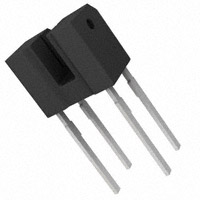
Transmissive Photosensors (Photo Interrupters)
CNA1311K
Photo Interrupter
For contactless SW, object detection
A side (1.5)
(0.15)
B side
Unit : mm
Overview
CNA1311K is an ultraminiature, highly reliable transmissive photosensor in which a high efficiency GaAs infrared light emitting diode chip and a high sensitivity Si phototransistor chip are integrated in a double molded resin package.
(1.8) 4.0 1.0 A
With gate A Side or B Side Optical center 2.6 (C0.5)
1.5
1.5
Slit width (0.15)
5.0 min. 3.3 2.3
(0.9)
1.5
2-0.4 A' *3.0 1 3 *2.0
Features
Ultraminiature : 2.6 × 4.0 mm (height : 3.3 mm) Highly precise position detection : 0.05 mm Gap width : 1.0 mm
Not soldered 1.0 max.
2-0.2+0.2 –0.1
Absolute Maximum Ratings (Ta = 25˚C)
Parameter Reverse voltage (DC) Input (Light Forward current (DC) emitting diode) Power dissipation Collector current Symbol Ratings VR IF PD*1 IC 6 50 75 20 35 6 75 –40 to +100 260 Unit V mA mW mA V V mW
2 4 Pin connection 1: Anode 3: Collecter 2: Cathode 4: Emitter (Note) 1. Tolerance unless otherwise specified is ±0.2 2. ( ) Dimension is reference 3. * is dimension at the root of leads
2
4
*1
Output (Photo Collector to emitter voltage VCEO transistor) Emitter to collector voltage VECO Collector power dissipation Operating ambient temperature Temperature Storage temperature Soldering temperature PC
*2
Input power derating ratio is 1.0mW/˚C at Ta ≥ 25˚C. *2 Output power derating ratio is 1.0mW/˚C at Ta ≥ 25˚C. *3 Soldering time is within 5 seconds.
Topr –25 to +85 Tstg Tsol*3
Electrical Characteristics (Ta = 25˚C)
Parameter Forward voltage (DC) Input characteristics Reverse current (DC) Output characteristics Collector cutoff current Symbol VF IR ICEO V R = 3V VCE = 20V 50 50 Conditions IF = 20mA min typ 1.2 max 1.4 10 100 600 0.4 Unit V µA nA µA V µs
Collector current IC VCE = 5V, IF = 5mA Transfer Collector to emitter saturation voltage VCE(sat) IF = 10mA, IC = 40µA characteristics Response time tr , tf* VCC = 5V, IC = 0.1mA, RL = 1000Ω
*
Switching time measurement circuit
Sig.IN VCC (Input pulse) Sig.OUT (Output pulse) 90% 10% td tr tf td : Delay time tr : Rise time (Time required for the collector current to increase from 10% to 90% of its final value) tf : Fall time (Time required for the collector current to decrease from 90% to 10% of its initial value)
,,
,,
50Ω
RL
,, ,, ,,,
˚C ˚C ˚C
Soldering bath
more than 1mm
,, ,
SEC. A-A' 1
(0.45)
2-0.5
3
1
�CNA1311K
Transmissive Photosensors (Photo Interrupters)
IF , IC — Ta
60 60
IF — VF
5 Ta = 25˚C
IC — IF
VCE = 5V Ta = 25˚C
IF , IC (mA)
50
IF
50
Forward current, collector current
40
IF (mA)
40
IC (mA) Collector current
0 0.4 0.8 1.2 1.6 2.0 2.4
4
3
30 IC
Forward current
30
2
20
20
10
10
1
0 – 25
0
20
40
60
80
100
0
0
0
5
10
15
20
25
Ambient temperature Ta (˚C )
Forward voltage VF (V)
Forward current IF (mA)
VF — Ta
1.6 3
IC — VCE
120 Ta = 25˚C IF = 50mA 100
IC — Ta
VCE = 5V IF = 5mA
VF (V)
1.2
10mA
IC (mA)
IC (%)
2
80
Forward voltage
0.8
Collector current
1mA
Relative output current
IF = 20mA 1 15mA 10mA 5mA 2mA 0 1 2 3 4 5 6
60
40
0.4
20
0 – 40 – 20
0
20
40
60
80
100
0
0 – 40 – 20
0
20
40
60
80
100
Ambient temperature Ta (˚C )
Collector to emitter voltage VCE (V)
Ambient temperature Ta (˚C )
ICEO — Ta
1 VCE = 20V 10 3
tr — IC
VCC = 5V 10 3
tf — IC
VCC = 5V
10 –1
ICEO (µA)
10 2
10 2
tr (µs)
tf (µs)
RL = 2kΩ 1kΩ 10 100Ω
10 –2
RL = 2kΩ 1kΩ 10 100Ω
Rise time
Dark current
10 –3
1 10 –4
Sig.IN Sig. OUT 50Ω
VCC Sig. OUT RL 90% 10%
Fall time
1
Sig.IN Sig. OUT 50Ω
VCC Sig. OUT RL 90% 10%
10 –5 – 40 – 20
, ,,
0
20
40
60
80
100
10 –1 10 –2
tr
tf
10
,,
10 –1 10 –2 10 –1
td
tr
1
td
tf
10
10 –1
1
Ambient temperature Ta (˚C )
Collector current IC (mA)
Collector current IC (mA)
2
�Transmissive Photosensors (Photo Interrupters)
CNA1311K
IC — d
100 100
IC — d
VCE = 5V Ta = 25˚C IF = 5mA VCE = 5V Ta = 25˚C IF = 5mA
Relative output current IC (%)
,,,
Criterion 0 d 0 0.4 0.8 1.2 1.6 2.0
80
Relative output current IC (%)
80 Criterion 0
60
60
40
40
20
20
0
0
0
0.4
Distance d (mm)
,, ,
d 0.8 1.2 1.6 2.0
Distance d (mm)
3
�
很抱歉,暂时无法提供与“CNA1311K”相匹配的价格&库存,您可以联系我们找货
免费人工找货