Product Specification
PE42423
UltraCMOS® SPDT RF Switch
100 MHz - 6 GHz
Product Description
Features
The PE42423 is a HaRP™ technology-enhanced
absorptive 50Ω SPDT RF switch designed for use in high
power and high performance WLAN 802.11 a/b/g/n/ac
applications such as carrier and enterprise Wi-Fi Products,
supporting bandwidths up to 6 GHz.
802.11 a/b/g/n/ac support
Wide supply range of 2.3V to 5.5V
+1.8V control logic compatible
Exceptional isolation
This switch features high linearity which remains invariant
across the full supply range. PE42423 also features
exceptional isolation, high power handling and is offered in
a 16-lead 3x3 mm QFN package. In addition, no external
blocking capacitors are required if 0V DC is present on the
RF ports.
47 dB @ 2.4 GHz
43 dB @ 6.0 GHz
High linearity across supply range
IIP3 of 65 dBm
IIP2 of 120 dBm
High power handling
38.5 dBm @ 2.4 GHz
37.0 dBm @ 6.0 GHz
Fast switching time of 500 ns
ESD performance
3kV HBM on RF pins to GND
1.5kV HBM on all pins
1kV CDM on all pins
The PE42423 is manufactured on PSemi’s UltraCMOS®
process, a patented variation of silicon-on-insulator (SOI)
technology on a sapphire substrate.
PSemi’s HaRP™ technology enhancements deliver high
linearity and excellent harmonics performance. It is an
innovative feature of the UltraCMOS® process, offering the
performance of GaAs with the economy and integration of
conventional CMOS.
Figure 2. Package Type
16-lead 3x3 mm QFN
Figure 1. Functional Diagram
RFC
ESD
RF2
RF1
ESD
ESD
50Ω
CMOS Control
Driver and ESD
LS CTRL
Document No. DOC-85742-2 │ www.psemi.com
VDD
50Ω
DOC-52425
©2017, 2019 pSemi Corp. All rights reserved.
Page 1 of 11
�PE42423
Product Specification
Table 1. Electrical Specifications Temp = 25°C, VDD = 3.3V
Parameter
Path
Condition
Operational frequency
Min
Typ
0.1
Unit
6
GHz
1.0
1.1
1.1
dB
dB
dB
Insertion loss
RFC–RFX
0.1–2.4 GHz
2.4–5.8 GHz
5.8–6.0 GHz
Isolation
RFX–RFX
0.1–2.4 GHz
2.4–5.8 GHz
5.8–6.0 GHz
49
39
39
51
41
41
dB
dB
dB
Isolation
RFC–RFX
0.1–2.4 GHz
2.4–5.8 GHz
5.8–6.0 GHz
44
39
40
47
41
43
dB
dB
dB
Return loss
(common and active port)
RFX
0.1–2.4 GHz
2.4–5.8 GHz
5.8–6.0 GHz
19
16
16
dB
dB
dB
Return loss (terminated port)
RFX
0.1–2.4 GHz
2.4–5.8 GHz
5.8–6.0 GHz
23
23
24
dB
dB
dB
Input 0.1 dB compression point1
RFC–RFX
0.6–4.0 GHz
39.5
dBm
Input IP32
RFC–RFX
0.8–2.7 GHz
65
dBm
2
RFC–RFX
0.8–2.7 GHz
120
dBm
50% CTRL to 90% or 10% of final value
500
Input IP2
Switching time
Notes:
0.80
0.95
0.95
Max
700
ns
1. The input 0.1dB compression point is a linearity figure of merit. Refer to Table 3 for the operating RF input power (50│ )
2. The input intercept point remains invariant over the full supply range as defined in Table 3
©2017, 2019 pSemi Corp. All rights reserved.
Page 2 of 11
Document No. DOC-85742-2 │ UltraCMOS® RFIC Solutions
�PE42423
Product Specification
4
GND
GND
13
CTRL
14
Min
Supply voltage
VDD
2.3
Supply current
IDD
Typ
120
Max
Unit
5.5
V
200
µA
Digital input high (CTRL)
VIH
1.17
3.6
V
GND
Digital input low (CTRL)
VIL
-0.3
0.6
V
11
RF2
RF input power, CW
0.1–0.6 GHz
0.6–4.0 GHz
4.0–6.0 GHz
10
GND
9
GND
Pin #
Pin Name
Description
1, 3, 4, 5,
6, 8, 9, 10,
12, 13
GND
Ground
2
RF11
RF port 1
7
RFC1
RF common
11
RF21
RF port 2
14
CTRL
Digital control logic input
RF input power, pulsed1
0.1–0.6 GHz
0.6–4.0 GHz
4.0–6.0 GHz
LS
16
VDD
Supply voltage (nominal 3.3V)
Pad
GND
Exposed pad: ground for proper operation
Note 1: RF pins 2, 7 and 11 must be at 0V DC. The RF pins do not require DC
blocking capacitors for proper operation if the 0V DC requirement is
met
27
dBm
Fig. 4 dBm
Fig. 4 dBm
PMAX,PULSED
RF input power into
terminated ports, CW
PMAX,TERM
TOP
-40
+25
22
dBm
+125
°C
Note 1: Pulsed, 5% duty cycle of 4620 µs period, 50│
Table 4. Absolute Maximum Ratings
Parameter/Condition
Logic Select - used to determine the
definition for the CTRL pin (see Table 5)
27
dBm
Fig. 4 dBm
Fig. 4 dBm
PMAX,CW
Operating temperature
range
Table 2. Pin Descriptions
15
Symbol
12
8
GND
Table 3. Operating Ranges
Parameter
GND
3
5
GND
Exposed
Ground Pad
7
2
RFC
RF1
6
1
GND
GND
15
16
VDD
Pin 1 dot
marking
LS
Figure 3. Pin Configuration (Top View)
Supply voltage
Digital input voltage (CTRL)
LS input voltage
Maximum input power
0.1–0.6 GHz
0.6–4.0 GHz
4.0–6.0 GHz
Symbol
Min
Max
Unit
VDD
-0.3
5.5
V
VCTRL
-0.3
3.6
V
VLS
-0.3
3.6
V
30
39
37.5
dBm
dBm
dBm
+150
°C
PMAX,ABS
Storage temperature range
TST
-65
1
ESD voltage HBM
RF pins to GND
All pins
VESD,HBM
3000
1500
V
V
ESD voltage MM2, all pins
VESD,MM
200
V
VESD,CDM
1000
V
3
ESD voltage CDM , all pins
Notes:
1. Human Body Model (MIL-STD 883 Method 3015)
2. Machine Model (JEDEC JESD22-A115)
3. Charged Device Model (JEDEC JESD22-C101)
Exceeding absolute maximum ratings may cause
permanent damage. Operation should be restricted
to the limits in the Operating Ranges table.
Operation between operating range maximum and
absolute maximum for extended periods may
reduce reliability.
Document No. DOC-85742-2 │ www.psemi.com
©2017, 2019 pSemi Corp. All rights reserved.
Page 3 of 11
�PE42423
Product Specification
Table 5. Control Logic Truth Table
Electrostatic Discharge (ESD) Precautions
®
When handling this UltraCMOS device, observe
the same precautions that you would use with
other ESD-sensitive devices. Although this device
contains circuitry to protect it from damage due to
ESD, precautions should be taken to avoid
exceeding the rating specified.
Latch-Up Avoidance
Unlike conventional CMOS devices, UltraCMOS
devices are immune to latch-up.
LS
CTRL
RFC-RF1
RFC-RF2
0
0
off
on
0
1
on
off
1
0
on
off
1
1
off
on
Moisture Sensitivity Level
®
Switching Frequency
The PE42423 has a maximum 25 kHz switching
rate. Switching frequency describes the time
duration between switching events. Switching time
is the time duration between the point the control
signal reaches 50% of the final value and the point
the output signal reaches within 10% or 90% of its
target value.
The Moisture Sensitivity Level rating for the
PE42423 in the 16-lead 3x3 mm QFN package is
MSL3.
Logic Select (LS)
The Logic Select feature is used to determine the
definition for the CTRL pin.
Figure 4. Power De-rating Curve for 600 MHz – 6 GHz
©2017, 2019 pSemi Corp. All rights reserved.
Page 4 of 11
Document No. DOC-85742-2 │ UltraCMOS® RFIC Solutions
�PE42423
Product Specification
Typical Performance Data @ 25°C and VDD = 3.3V unless otherwise specified
Figure 5. Insertion Loss vs. Temp (RFC–RFX)
25
125
2.3
0
0
-0.2
-0.2
-0.4
-0.4
-0.6
-0.6
Insertion Loss [dB]
Insertion Loss [dB]
-40
Figure 6. Insertion Loss vs. VDD (RFC–RFX)
-0.8
-1
-1.2
-1.6
-1.6
-1.8
-1.8
1
2
3
Frequency [GHz]
4
5
-40
25
-2
6
Figure 7. RFX Port Return Loss vs. Temp
0
1
2
3
Frequency [GHz]
4
5
6
5
6
Figure 8. RFX Port Return Loss vs. VDD
125
2.3
0
0
-5
-5
-10
-10
-15
-15
Return Loss [dB]
Return Loss [dB]
-1
-1.2
-1.4
0
5.5
-0.8
-1.4
-2
3.3
-20
-25
-30
3.3
5.5
-20
-25
-30
-35
-35
-40
0
1
2
3
Frequency [GHz]
Document No. DOC-85742-2 │ www.psemi.com
4
5
6
-40
0
1
2
3
4
Frequency [GHz]
©2017, 2019 pSemi Corp. All rights reserved.
Page 5 of 11
�PE42423
Product Specification
Typical Performance Data @ 25°C and VDD = 3.3V unless otherwise specified
Figure 9. Terminated Port Return Loss vs. Temp
(RFX Active)
25
125
2.3
0
0
-5
-5
-10
-10
-15
-15
Return Loss [dB]
Return Loss [dB]
-40
Figure 10. Terminated Port Return Loss vs. VDD
(RFX Active)
-20
-25
-25
-30
-35
-35
-40
0
1
2
3
4
5
6
0
1
2
3
Frequency [GHz]
-40
25
4
5
6
5
6
Frequency [GHz]
Figure 11. Isolation vs. Temp
(RFX–RFX, RFX Active)
Figure 12. Isolation vs. VDD
(RFX–RFX, RFX Active)
2.3
125
0
0
-10
-10
-20
-20
-30
-30
Isolation [dB]
Isolation [dB]
5.5
-20
-30
-40
3.3
-40
-50
3.3
5.5
-40
-50
-60
-60
-70
-70
-80
-80
-90
-90
0
1
2
3
Frequency [GHz]
©2017, 2019 pSemi Corp. All rights reserved.
Page 6 of 11
4
5
6
0
1
2
3
4
Frequency [GHz]
Document No. DOC-85742-2 │ UltraCMOS® RFIC Solutions
�PE42423
Product Specification
Typical Performance Data @ 25°C and VDD = 3.3V unless otherwise specified
Figure 13. Isolation vs. Temp
(RFC–RFX, RFX Active)
25
125
2.3
0
0
-10
-10
-20
-20
-30
-30
Isolation [dB]
Isolation [dB]
-40
Figure 14. Isolation vs. VDD
(RFC–RFX, RFX Active)
-40
-50
5.5
-40
-50
-60
-60
-70
-70
-80
-80
-90
3.3
-90
0
1
2
3
Frequency [GHz]
Document No. DOC-85742-2 │ www.psemi.com
4
5
6
0
1
2
3
4
5
Frequency [GHz]
©2017, 2019 pSemi Corp. All rights reserved.
Page 7 of 11
6
�PE42423
Product Specification
Evaluation Kit
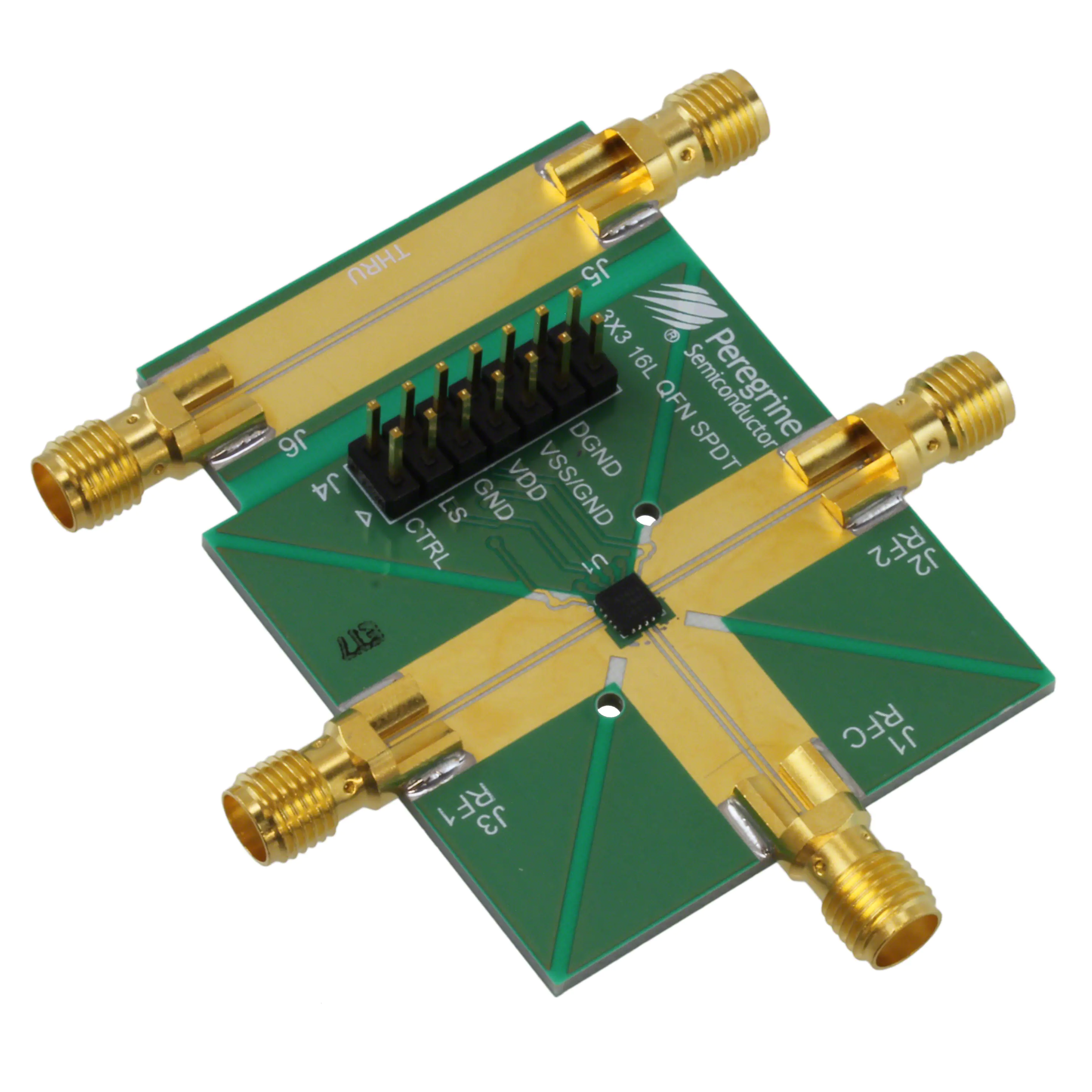
Figure 15. Evaluation Kit Layout
The SPDT switch evaluation board was designed
to ease customer evaluation of PSemi’s
PE42423. The RF common port is connected
through a 50│ transmission line via the SMA
connector, J1. RF1 and RF2 ports are connected
through 50│ transmission lines via SMA
connectors J2 and J3, respectively. A 50│
through transmission line is available via SMA
connectors J5 and J6, which can be used to
de-embed the loss of the PCB. J4 provides DC
and digital inputs to the device.
For the true performance of the PE42423 to be
realized, the PCB should be designed in such a
way that RF transmission lines and sensitive DC
I/O traces are heavily isolated from one another.
PRT-30186
©2017, 2019 pSemi Corp. All rights reserved.
Page 8 of 11
Document No. DOC-85742-2 │ UltraCMOS® RFIC Solutions
�PE42423
Product Specification
Figure 16. Evaluation Board Schematic
DOC-11027
Notes: 1. Use PRT-30186-2 PCB
2. CAUTION: Contains parts and assemblies susceptible to damage
by electrostatic discharge (ESD)
Document No. DOC-85742-2 │ www.psemi.com
©2017, 2019 pSemi Corp. All rights reserved.
Page 9 of 11
�PE42423
Product Specification
Figure 17. Package Drawing
16-lead 3x3 mm QFN
DOC-58196
Figure 18. Top Marking Specifications
42423
YYWW
ZZZZZ
= Pin 1 designator
YYWW = Date code
ZZZZZ = Last five digits of lot number
17-0009
©2017, 2019 pSemi Corp. All rights reserved.
Page 10 of 11
Document No. DOC-85742-2 │ UltraCMOS® RFIC Solutions
�PE42423
Product Specification
Figure 19. Tape and Reel Specifications
Notes: 1. 10 sprocket hole pitch cumulative tolerance ±0.2
2. Camber in compliance with EIA 481
3. Pocket position relative to sprocket hole measured
as true position of pocket, not pocket hole
Ao = 3.30
Bo = 3.30
Ko = 1.10
Pin 1
Top of
Device
Device Orientation in Tape
Table 6. Ordering Information
Order Code
Description
Package
Shipping Method
PE42423B-Z
PE42423 SPDT RF switch
Green 16-lead 3x3 mm QFN
3000 units/T&R
EK42423-03
PE42423 Evaluation kit
Evaluation kit
1/Box
Sales Contact and Information
For sales and contact information please visit www.psemi.com.
Document No. DOC-85742-2 │ www.psemi.com
©2017, 2019 pSemi Corp. All rights reserved.
Page 11 of 11
�