0
登录后你可以
  • 下载海量资料
  • 学习在线课程
  • 观看技术视频
  • 写文章/发帖/加入社区
会员中心
创作中心
发布
  • 发文章

  • 发资料

  • 发帖

  • 提问

  • 发视频

创作活动
FNDDR1133

FNDDR1133

  • 厂商:

    PERICOM

  • 封装:

  • 描述:

    FNDDR1133 - 3.3V CMOS Low-Jitter 133.330 MHz DDR XO - Pericom Semiconductor Corporation

  • 详情介绍
  • 数据手册
  • 价格&库存
FNDDR1133 数据手册
TM Application Specific Crystal Oscillator 7.0 x 5.0mm 3.3V CMOS Low-Jitter 133.330 MHz DDR XO FNDDR1133 7.0 x 5.0mm Ceramic SMD ASSP XO™ for Networking Package: Product Features • Very low Pk to Pk jitter - 30ps Max • Low output current - 20mA Max • Low power standby mode • RoHS Compliant Recommended Land Pattern: Product Description This is an enhanced high frequency 3.3V, 133.33MHz crystal clock oscillator with superb jitter and low operating current for DDR cache memory applications in Serial Attached SCSI RAID controller/Host Bus Adapter. Pin Functions: Pin Function Applications • Serial Attached SCSI 3G/6G RAID Controller • Serial Attached SCSI 3G/6G Host Bus Adapter 1 2 3 4 OE Function Ground Clock Output V DD *Extended high frequency power decoupling is recommended (see test circuit for minimum recommendation). To ensure optimal performance, do not route RF traces beneath the package. Part Ordering Information: FNDDR1133 SaRonix-eCera™ is a Pericom® Semiconductor company • US: +1-408-435-0800 TW: +886-3-4518888 10-0020 • www.pericom.com A ll specifications are subject to change without notice. FNDDR1133 Rev C 04/13/10 1 3.3V CMOS Low-Jitter 133.330 MHz DDR XO FNDDR1133 TM Application Specific Crystal Oscillator 7.0 x 5.0mm Electrical Performance Parameter Min. Typ. Max. Units Notes Output Frequency Supply Voltage V DD Supply Current, Output Enabled Supply Current, Output Disabled Frequency Stability Operating Temperature Range Output Logic 0, VOL Output Logic 1, VOH Output Load Duty Cycle Rise and Fall Time Jitter, pk-pk 45 90% V DD -20 2.97 133.330 3.3 3.63 20 10 ±50 +70 10% V DD 15 55 2 30 MHz V mA µA ppm °C V V pF % ns ps Measured 50% V DD Measured 20/80% of waveform 100.000 random periods See Note 1 below Notes: 1. Stability includes all combinations of operating temperature, load changes, rated input (supply) voltage changes, initial calibration tolerance (25°C), aging (1 year at 25°C average effective ambient temperature), shock and vibration. 2. For specifications othere than those listed, please contact sales. Output Enable / Disable Function Parameter Min. Typ. Max. Units Notes Input Voltage (pin 1), Output Enable Input Voltage (pin 1), Output Disable (low power standby) Internal Pullup Resistance Output Disable Delay Output Enable Delay 0.7 V DD 0.3 V DD 30 200 2 V V kΩ ns ms or open Output is Hi-Z Absolute Maximum Ratings Parameter Min. Typ. Max. Units Notes Storage Temperature -55 +125 °C For the latest product information visit: http://www.pericom.com/products/timing/oscillators/FNDDR1133/ For test circuit go to: http://www.pericom.com/pdf/sre/tc_hcmos.pdf For soldering reflow profile and reliability test ratings go to: http://www.pericom.com/pdf/sre/reflow.pdf For tape and reel information go to: http://www.pericom.com/pdf/sre/tr_7050.pdf SaRonix-eCera™ is a Pericom® Semiconductor company • US: +1-408-435-0800 TW: +886-3-4518888 10-0020 • www.pericom.com A ll specifications are subject to change without notice. FNDDR1133 Rev C 04/13/10 2
FNDDR1133
1. 物料型号: - 型号:FNDDR1133

2. 器件简介: - 该器件是一个3.3V CMOS低抖动133.330 MHz DDR晶振,具有超低抖动和低工作电流,适用于串行连接SCSI RAID控制器/主机总线适配器中的DDR缓存内存应用。

3. 引脚分配: - 引脚1:OE功能(输出使能) - 引脚2:地(GND) - 引脚3:时钟输出(Clock Output) - 引脚4:电源电压(VDD)

4. 参数特性: - 输出频率:133.330 MHz - 供电电压(VDD):2.97V至3.63V - 输出使能时供电电流:最大20 mA - 输出禁用时供电电流:10 µA - 频率稳定性:±50 ppm - 工作温度范围:-20°C至+70°C - 输出逻辑0(VOL):10% VDD - 输出逻辑1(VOH):90% VDD - 输出负载:15 pF - 占空比:45%至55%(在50% VDD下测量) - 上升和下降时间:2 ns(在20%至80%波形下测量) - 抖动,峰峰值:30 ps(在100,000个随机周期下测量)

5. 功能详解: - 该晶振具有非常低的峰峰抖动(最大30ps),低输出电流(最大20mA),并且有低功耗待机模式。它符合RoHS标准。

6. 应用信息: - 适用于串行连接SCSI 3G/6G RAID控制器和主机总线适配器。
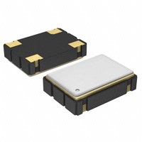
7. 封装信息: - 封装类型为7.0 x 5.0mm的陶瓷表面贴装(SMD)。
FNDDR1133 价格&库存

很抱歉,暂时无法提供与“FNDDR1133”相匹配的价格&库存,您可以联系我们找货

免费人工找货