IB ST (ZF) 24 DO 32/2
Digital Output Module With 32 Channels
5 0 1 7 C 0 0 0
Data Sheet 5017C
Terminal Assignment
8 8
8 9
9 2
9 3
9 6
6 5
6 8
6 9
7 2
7 3
7 6
7 7
8 0
B
F
F
F
F
U s 1
IB S T M E 2 4 D O
U S
E 1
U s 2
E 2
E
T E R
U S
E
IN
U S
E
E
U S
Terminals
U s 3
E 3
1 0
1 1
1 2
4 2
4 3
4 4
3 2 /2 , O rd . N o .: 2 7 5 4 3 7 0
U s 4
E 4
1 3
1 4
1 5
1 6
4 5
4 6
4 7
4 8
U L
1
2
3
4
5
6
7
8
9
3 3
3 4
3 5
3 6
3 7
3 8
3 9
4 0
4 1
0 0 0 1 0 2 0 3 0 4 0 5 0 6 0 7 0 8 0 9 1 0
1
2
3
4
5
6
7
8
9
1 0
1 1
1 2
1 3
1 4
1 5
1 6
1 7
1 8
1 9
2 0
2 1
2 2
2 3
2 4
2 5
2 6
2 7
2 8
2 9
3 0
3 1
3 2
3 3
3 4
3 5
3 6
3 7
3 8
3 9
4 0
4 1
4 2
4 9
5 0
5 4
5 5
5 6
5 2
5 3
5 7
5 8
4 4
4 5
4 6
4 7
4 8
5 9
6 0
6 1
6 2
6 3
6 4
17 through 32 Ground contacts for actuators
and
49 through 64
65, 69, 73
and 77
Supply voltages for the
module (Us1 through Us4)
81, 85, 89
and 93
Ground contacts for the
module (Us1 through Us4)
Local Diagnostic and Status Indicators
5 0 1 7 C 0 0 1
in
ec
Figure1
5 1
4 3
1 through 16 Digital signal outputs
and
33 through 48
ne
3 2 d ig ita l O u tp u t, 2 4 V D C , M o d u le Id e n t.: 1 8 9
po
B A
om
C C
Assignment
co
8 5
s.
8 4
nt
8 1
U S
m
03/2000
Des. Color
UL
Green Supply voltage for the module
electronics
CC
Green Cable check
BA
Green Bus active
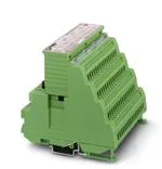
IB ST 24 DO 32/2 module
on
l
This data sheet is intended to be used
in conjunction with the
IBS SYS PRO UM E I/O
Systems Manual.
Ground the mounting rail. The module
is grounded by snapping it onto the
mounting rail.
Meaning
Usn Green 24 V I/O supply voltage, group n
En
xx
Red
Error in group n
Yellow Output status (for the channel
on terminal xx)
The numbering of the yellow status
indicators corresponds to the screw or
spring-clamp terminal. It does not
apply to the channel bit mapping.
5017C
1
�IB ST (ZF) 24 DO 32/2
Internal Circuit Diagram
8 4
8 1
8 5
8 8
9 2
8 9
9 3
9 6
6 5
6 8
S T lo c a l b u s
6 9
7 2 7 3
7 6
7 7
8 0
S T lo c a l b u s
S U P I 3
5 V
O U T
m
IN
4 9
1 9
3 4
3 5
O U T O U T
5 0
5 1
2 0
2 1
3 6
3 7
O U T
O U T
5 2
5 3
8
9
O U T O U T
6
7
O U T
O U T
2 2
2 4
2 3
1 0
3 8
3 9
O U T O U T
5 4
1 5
2 6
2 7
3 1
4 2
4 3
O U T O U T
2 5
4 0
4 1
O U T
O U T
5 5
1 1
1 2
5 6
5 7
s.
5
O U T
O U T O U T
5 8
5 9
1 3
O U T O U T
ne
1 8
4
O U T
nt
3 3
O U T
3
po
1 7
2
O U T O U T
om
1
O U T
co
5 V
9 V /5 V
2 8
2 9
4 4
4 5
1 4
1 6
O U T O U T
O U T
3 0
3 2
4 6
4 7
4 8
O U T O U T
O U T O U T
O U T
6 0
6 2
6 4
6 1
6 3
5 0 1 7 D 0 0 4
Internal wiring of the module terminals
in
ec
Figure 2
F
F
F
F
E
U S
E
U S
E
U S
E
U S
on
l
The limit values of the
electromagnetic noise emission
according to EN 55011, Class A are
only kept by the modules if they are
installed in a grounded, metal control
cabinet.
2
5017C
�IB ST (ZF) 24 DO 32/2
Electrical Isolation of the Individual Function Areas
IN T E R B U S
S T lo c a l b u s
(IN )
IN T E R B U S
S T lo c a l b u s
(O U T )
B u s in te r fa c e
(m ic r o p r o c e s s o r a n d S U P I)
8 d ig ita l
o u tp u ts e a c h
A
I/O
d e v ic e
in te r fa c e
I/O
d e v ic e
in te r fa c e
B
I/O
d e v ic e
in te r fa c e
E le c tr ic a l is o la tio n b e tw e e n
a re a s A a n d B
m
I/O
d e v ic e
in te r fa c e
s.
co
2 4 V D C
s u p p ly
nt
P E p o te n tia l
Electrical isolation of the single function areas
ne
Figure 3
5 0 1 7 C 0 0 5
po
Connection Examples
F
F
7 3
7 6
IB S T M E 2 4 D O
E 2
on
l
U S 2
U S 3
E 3
7 7
8 0
3 2 /2 , O rd . N o .: 2 7 5 4 3 7 0
U S 4
E 4
8 8
8 9
9 2
U S
F
9 3
9 6
U S
F
U S
F
8 5
6 5
IN
6 8
T E R
U S 1
B
6 9
7 2
E 1
7 3
7 6
IB S T M E 2 4 D O
U S
U S 2
E 2
U S 3
E 3
7 7
8 0
3 2 /2 , O rd . N o .: 2 7 5 4 3 7 0
U S 4
E 4
5 0 1 7 C 0 0 6
Connection of the supply voltage and potential jumpering
Potential jumpering:
Between terminals 65, 69, 73 and 77
(Us1 through Us4) and 81, 85, 89 and
93 (^), an external jumper is required
on the screw terminal module in order
to supply all isolated groups from the
same voltage source or to connect
5017C
8 4
U S
E
7 2
8 1
E
E 1
6 9
9 6
U S
E
U S
9 3
E
B
9 2
C u r r e n t c a r r y in g c a p a c ity : 1 0 A m a x im u m
E
Figure 4
U S
E
U S 1
8 9
E
E
6 8
T E R
8 8
U S
6 5
IN
8 5
In te r n a l ju m p e r
_
F
8 4
U S
F
8 1
+
F
_
in
ec
+
om
Connection of the Supply Voltage and Potential Jumpering
additional modules.
However, for the spring-clamp terminal module,
external jumpers are required between terminals
68 and 69, 72 and 73 and 76 and 77 for Us1
through Us4 and 84 and 85, 88 and 89 and 92
and 93 for ground (^).
3
�IB ST (ZF) 24 DO 32/2
Typical Connection of the Supply and Actuators
U s 2
E 2
U s 3
E 3
2
3
4
5
6
7
8
9
3 3
3 4
3 5
3 6
3 7
3 8
3 9
4 0
4 1
0 0 0 1 0 2 0 3 0 4 0 5 0 6 0 7 0 8 0 9 1 0
1 0
1 1
2
3
4
1 8
1 9
3 3
3 4
3 5
a .9
Figure 5
O U T
O U T
on
l
4 9
5 0
5 1
6
a .6
7
8
a .5
a .4
2 0
2 1
2 2
2 3
2 4
3 6
3 7
3 8
3 9
4 0
5 4
5 5
5 6
a .8
in
ec
a .1 1 a .1 0
5
a .7
om
1 7
5 2
a .3
5 3
a .2
a .1
U s 4
4 3
E 4
1 2
1 3
4 4
4 5
1 4
1 5
1 6
4 6
4 7
4 8
9
a .0
1 0
1 1
1 2
b .1 5 b .1 4 b .1 3 b .1 2
1 3
1 4
1 5
1 6
b .7
b .6
b .5
b .4
2 5
2 6
2 7
2 8
2 9
3 0
3 1
3 2
4 1
4 2
4 3
4 4
4 5
4 6
4 7
4 8
5 9
6 0
6 1
6 2
6 3
6 4
b .1 1 b .1 0
5 7
5 8
b .9
b .8
b .3
b .2
b .1
b .0
W ir e e x te r n a lly
C o n n e c te d in te r n a lly
5 0 1 7 C 0 0 2
Typical digital actuator connections
Do not supply an external voltage to
an output. Otherwise, the module may
be damaged.
4
4 2
3 2 /2 , O rd . N o .: 2 7 5 4 3 7 0
3 2 d ig ita l O u tp u t, 2 4 V D C , M o d u le Id e n t.: 1 8 9
po
1
a .1 5 a .1 4 a .1 3 a .1 2
8 0
U S
nt
1
ne
B A
7 7
IB S T M E 2 4 D O
U S
E 1
U L
C C
7 6
9 6
O U T
B
F
F
U s 1
U S
9 3
E
T E R
7 3
9 2
E
IN
7 2
E
U S
8 9
O U T
6 9
8 8
m
6 8
E
U S
8 5
co
6 5
8 4
_
+
s.
8 1
_
+
F
_
+
F
_
+
The module terminals are assigned to
the two process data words. The label
a.xx/b.xx refers to the process data
word. The numbering refers to the bit
of the process data words.
5017C
�IB ST (ZF) 24 DO 32/2
Increasing the Current Carrying Capacity
M o d u le
te r m in a ls
4 A per group. All channels connected in parallel
must have the same reference ground. Changes
to the status of the parallel connected channels
(set or reset) must always be simultaneous
because staggered changes in status could lead
to an overload on the outputs.
m
To increase the current carrying capacity for
ohmic or lamp load, two or more channels can
be connected in parallel. Connect each of the
channels with a serial diode (see Figure 6).
When selecting the diodes, ensure a sufficient
current carrying capacity (minimum 500 mA)
and do not exceed the maximum total current of
s.
co
E x te rn a l
d io d e s
Figure 6
5 0 1 7 C 0 0 7
om
po
ne
nt
A c tu a to r
c o n n e c tio n
Parallel connection of outputs via external protective diodes
in
ec
Installation Check With External Voltage
on
l
If an external voltage is connected to
the actuators during the installation
check, the module electronics must
be removed from the terminal block.
Otherwise, the module may be
damaged.
5017C
5
�IB ST (ZF) 24 DO 32/2
Programming Data
BDhex (189dec)
Length code
02hex
Input address area
0 bytes
Output address area
4 bytes
Parameter channel
(PCP)
0 bytes
Register length (bus)
4 bytes
co
m
ID code
Assignment of the Module Terminals to the INTERBUS Reference
Word x
15 14 13 12 11 10 9
Byte
6
5
4
Terminal (signal) 1
2
3
4
Terminal point
(ground)
Word
Bit
Terminal
7
Terminal (signal) 9
on
l
Terminal point
(ground)
6
1
0
5
4
3
2
1
0
2
1
0
Byte 1
7
6
5
4
3
33 34 35 36 5
6
7
8
37 38 39 40
Word x + 1
15 14 13 12 11 10 9
Byte
Bit
2
6
17 18 19 20 49 50 51 52 21 22 23 24 53 54 55 56
in
ec
INTERBUS
reference
3
7
po
Terminal
7
om
Bit
Byte 0
8
nt
Bit
s.
Word
ne
INTERBUS
reference
8
7
6
5
Byte 0
6
5
4
3
4
3
2
1
0
2
1
0
Byte 1
2
1
0
7
6
5
4
3
10 11 12 41 42 43 44 13 14 15 16 45 46 47 48
25 26 27 28 57 58 59 60 29 30 31 32 61 62 63 64
5017C
�IB ST (ZF) 24 DO 32/2
Technical Data
General
118 mm x 116 mm x 117 mm
(4.646 in. x 4.567 in. x 4.606 in.)
Weight
790 g, typical
Connection type of the actuators
2-wire technology
Operating mode
Process data operation with 2 words
Total power consumption
See Table "Power Consumption" on page 8
Permissible operating temperature
0°C to 55°C (32°F to 131°F)
Permissible storage temperature
-20°C to 70°C (-4°F to 158°F)
Humidity
75% on average; 85% occasionally,
no condensation
Air pressure (operation)
From 86 kPa to 108 kPa, 1500 m (4921.260 ft.)
above sea level
ne
nt
s.
co
m
Housing dimensions (width x height x depth)
Bus/output groups
Test voltage
po
Electrical isolation (via optocoupler)
500 V AC, 1 min, 50 Hz
500 V AC, 1 min, 50 Hz
Output group/output group
500 V AC, 1 min, 50 Hz
Degree of protection
Class of protection
om
Output groups/protective conductor
IP 20, IEC 60529
Class 3, VDE 0106; IEC 60536
Via DIN rail
Preferred installation position
Panel mounting
Interface
in
ec
Protective ground connection
on
l
INTERBUS ST interface
5017C
ST cable (supplied with the module)
7
�IB ST (ZF) 24 DO 32/2
Logic voltage
9 V DC
Current consumption from the local bus
100 mA, maximum
Power consumption from the local bus
1 W, maximum
I/O supply voltage US
24 V DC
Current consumption of US
200 mA, typical
co
Supply of the Module Electronics Through the Bus Terminal Module
9V
Current consumption
100 mA, maximum
Power consumption
1.0 W, maximum
nt
s.
Logic voltage
I/O Supply Voltage (Us)
24 V DC
ne
Nominal value
Permissible voltage range
20 V DC to 30 V DC, ripple included
3.6 Vpp within the permissible voltage range
po
Permissible ripple
Electrical isolation to the bus
Test voltage
4
om
Number of isolated groups
in
ec
Protection against polarity reversal
Surge voltage protection
Number
on
l
Digital Outputs
m
Power Consumption
Through optocouplers
500 V AC (50 Hz for 1 min.)
Through diode and fuse connected in series
Fuses in the terminal block base
IBS TR5 5 AT
32 (8 for each group)
Minimum output voltage at nominal current
US minus 1 V
Short-circuit protection
Electronic, for each channel
Nominal current per channel
0.5 A, maximum
Short-circuit current protection
0.75 A, minimum
Minimum output current
1 mA
Output current per group
4 A for four channels, maximum
Output current per module
8 A, maximum
Short-circuit protection
Electronic, for each channel
8
5017C
�IB ST (ZF) 24 DO 32/2
(Continued)
Coincidence factor
50% at 24 V DC
Permissible load per output
Ohmic load 12 W
Lamp load 12 W
Inductive load (1.2 H; 48 Ohm) 12 VA
Permissible inductive breaking energy
200 mJ maximum
Limitation of the demagnetization voltage
induced on circuit interruption
USminus 45 V minimum
Behavior on overload
Autorestart
Behavior when ground connection interrupted
Disconnection of outputs
Permissible switching frequency
On ohmic load (48 Ohm), maximum 300 Hz
On inductive load (1.2 H; 48 Ohm),
maximum 0.5 Hz
I [A ]
ne
Derating curve for total output current (maximum
4 A per group)
nt
s.
co
m
Digital Outputs
6
4
2
in
ec
om
po
8
1 0
2 0
3 0
4 0
5 0
6 0
T [° C ]
5 0 1 7 C 0 0 3
on
l
Module Error Messages
Failure of the I/O supply voltage
No
Breakdown of the fuse for the I/O supply voltage No
Overtemperature of the output driver
Yes
Short circuit/overload of an output
Yes
5017C
9
�IB ST (ZF) 24 DO 32/2
Ordering Data
Description
Order Designation
Order No.
27 54 32 5
Digital output module (spring-clamp terminals) IB ST ZF 24 DO 32/2
27 50 63 3
Module electronics
IB STME 24 DO 32/2
27 54 37 0
Replacement terminal block (screw-clamp
terminals)
IB STTB 24 DO 32/2
27 53 03 8
Replacement terminal block (spring-clamp
terminals)
IB STTB ZF 24 DO 32/2
m
Digital output module (screw-clamp terminals) IB ST 24 DO 32/2
on
l
in
ec
om
po
ne
nt
s.
co
27 50 52 3
10
5017C
�on
l
in
ec
om
po
ne
nt
s.
co
m
IB ST (ZF) 24 DO 32/2
5017C
11
�12
© Phoenix Contact 03/2000 TNR 92 65 69 7
s.
nt
ne
po
om
in
ec
on
l
co
m
IB ST (ZF) 24 DO 32/2
5017C
�