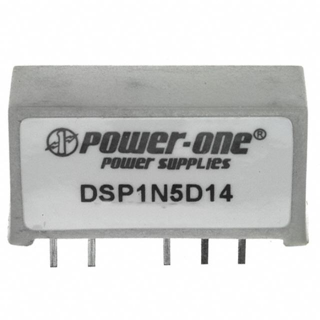
The DSP1D Series is specifically designed to convert a nominal 5 volt
input into two isolated output voltages.
The dual semi-regulated output voltages were designed to allow
analog circuits and three-terminal regulators to operate within their
most efficient input voltage range.
This series achieves high power densities through the use of 350 kHz
fixed-frequency switching converters.
RoHS lead solder exemption compliant
Up to 1 Watt unregulated output power
Single-In-Line package
Four-terminal operation
Efficiencies to 70%
Output Voltages: 5V, 7V, 12V, 14V, 15V, 17V
700 V isolation
-40 °C to +85 °C operation
�DSP1D Series
2
INPUT RANGE [VDC]
OUTPUT
MODEL
MIN
MAX
[VDC]
[mA]
POWER [W]
xxxx Model numbers highlighted in yellow are not recommended for new designs.
PARAMETER
CONDITIONS / DESCRIPTION
MIN
TYP
MAX
UNITS
Isolation
Isolation Voltage
Capacitance
VDC
500
Input to Output
10
pF
40
kΩ
Output Trim Function
Input Resistance
Programming Range
+5, -34
%
Environmental
Case Operating Range (TC)2
-40
85
°C
Storage Range
-55
105
°C
Line Regulation
Load Regulation
20% to 100% Load
1
%
5
%
700,000
hrs
0.1/28
oz/g
General
MTBF
Calculated
Weight
Case Material
Non Conductive Plastic
NOTES
1
2
All parameters measured at Tc = 25 °C, nominal input voltage and full rated load unless otherwise noted.
Derate output power linearly to 0.6 watts from 70 °C to 85 °C.
tech.support@psbel.com
�DSP1D Series
3
EXTERNAL CAPACITANCE REQUIREMENTS
Output filtering is required for operation. A minimum of 10 F is specified for optimal performance. Output capacitance may be
increased for additional filtering, and should not exceed 400 μF. To meet the reflected ripple requirements of the converter, an input
impedance of less than 0.5 Ohms from DC to 350 kHz is required. If a capacitive input source is farther than 2” from the converter,
it is recommended to use a 10 μF, 25 V solid tantalum capacitor.
REGULATION
This converter uses a semi-regulated design. The output will vary as the load is changed, with output decreasing with increasing
load. Additionally, output voltage will change in proportion to a change in input voltage. The typical output voltage will change 1%
for each 1% change in input voltage.
Figure 1. Typical Performance (Tc = 25°C)
DSP1 SERIES BLOCK DIAGRAM
+ INPUT 1
OSCILLATOR
DRIVER
5
+ OUTPUT
4
CMN
3
– OUTPUT
– INPUT 2
Figure 2. Block Diagram
Europe, Middle East
+353 61 225 977
North America
+1 408 785 5200
© 2016 Bel Power Solutions & Protection
BCD.00866_AA
Asia-Pacific
+86 755 298 85888
�DSP1D Series
4
PIN
1
FRONT VIEW
2
0.40
(10.16)
3
0.02
(0.51)
RT
4
SIDE
5
FUNCTION
+INPUT
-INPUT
- OUT
COMMON
+OUT
VIEW
Mechanical tolerances unless otherwise
noted:
0.000
1
2
3
4
5
X.XX dimensions: ±0.020 inches
X.XXX dimensions: ±0.010 inches
PINS: 0.02 (0.51) x 0.01 (0.25)
LENGTH (TYPICAL): 0.15 (3.81)
Figure 3. Mechanical Dimensions
NUCLEAR AND MEDICAL APPLICATIONS - Products are not designed or intended for use as critical components in life support systems,
equipment used in hazardous environments, or nuclear control systems.
TECHNICAL REVISIONS - The appearance of products, including safety agency certifications pictured on labels, may change depending on
the date manufactured. Specifications are subject to change without notice.
tech.support@psbel.com
�
很抱歉,暂时无法提供与“DSP1N5D14”相匹配的价格&库存,您可以联系我们找货
免费人工找货