CM100DY-24A
Powerex, Inc., 200 E. Hillis Street, Youngwood, Pennsylvania 15697-1800 (724) 925-7272
Dual IGBTMOD™ A-Series Module
100 Amperes /1200 Volts
A F E F E
G2 E2
G J H G
B
N
C2E1 E2 C1 E1 G1
K L (2 PLACES) P
K D
K M NUTS (3 PLACES)
Q
P
Q
P
T THICK U WIDTH
S C V LABEL R
G2 E2
Description: Powerex IGBTMOD™ Modules are designed for use in switching applications. Each module consists of two IGBT Transistors in a half-bridge configuration with each transistor having a reverseconnected super-fast recovery free-wheel diode. All components and interconnects are isolated from the heat sinking baseplate, offering simplified system assembly and thermal management. Features: £ Low Drive Power £ Low VCE(sat) £ Discrete Super-Fast Recovery Free-Wheel Diode £ Isolated Baseplate for Easy Heat Sinking Applications: £ AC Motor Control £ UPS £ Battery Powered Supplies Ordering Information: Example: Select the complete part module number you desire from the table below -i.e. CM100DY-24A is a 1200V (VCES), 100 Ampere Dual IGBTMOD™ Power Module.
Type CM Current Rating Amperes 100 VCES Volts (x 50) 24
C2E1
E2
C1
E1 G1
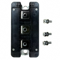
Outline Drawing and Circuit Diagram Dimensions A B C D E F G H J K Inches 3.70 1.89 3.15±0.01 0.67 0.91 0.16 0.71 0.51 0.47 Millimeters 94.0 48.0 80.0±0.25 17.0 23.0 4.0 18.0 13.0 12.0 Dimensions L M N P Q R S T U V Inches 0.26 Dia. M5 Metric 0.79 0.63 0.28 0.83 0.30 0.02 0.110 0.16 Millimeters Dia. 6.5 M5 20.0 16.0 7.0 21.2 7.5 0.5 2.8 4.0
1.14+0.004/-0.02 29.0+0.1/-0.5
1
�Powerex, Inc., 200 E. Hillis Street, Youngwood, Pennsylvania 15697-1800 (724) 925-7272 CM100DY-24A Dual IGBTMOD™ A-Series Module 100 Amperes /1200 Volts
Absolute Maximum Ratings, Tj = 25°C unless otherwise specified
Ratings Junction Temperature Storage Temperature Collector-Emitter Voltage (G-E Short) Gate-Emitter Voltage (C-E Short) Collector Current (DC, TC = 84°C*) Peak Collector Current Emitter Current*** (TC = 25°C) Peak Emitter Current*** Maximum Collector Dissipation (TC = 25°C*, Tj ≤ 150°C) Mounting Torque, M5 Main Terminal Mounting Torque, M6 Mounting Weight Isolation Voltage (Main Terminal to Baseplate, AC 1 min.) Symbol Tj Tstg VCES VGES IC ICM IE IEM PC — — — VISO CM100DY-24A –40 to 150 –40 to 125 1200 ±20 100 200** 100 200** 672 30 40 310 2500 Units °C °C Volts Volts Amperes Amperes Amperes Amperes Watts in-lb in-lb Grams Volts
Static Electrical Characteristics, Tj = 25°C unless otherwise specified
Characteristics Collector-Cutoff Current Gate Leakage Current Gate-Emitter Threshold Voltage Collector-Emitter Saturation Voltage Total Gate Charge Emitter-Collector Voltage** Symbol ICES IGES VGE(th) VCE(sat) QG VEC Test Conditions VCE = VCES, VGE = 0V VGE = VGES, VCE = 0V IC = 10mA, VCE = 10V IC = 100A, VGE = 15V, Tj = 25°C IC = 100A, VGE = 15V, Tj = 125°C VCC = 600V, IC = 100A, VGE = 15V IE = 100A, VGE = 0V Min. — — 6.0 — — — — Typ. — — 7.0 2.1 2.4 500 — Max. 1.0 0.5 8.0 3.0 — — 3.8 Units mA µA Volts Volts Volts nC Volts
Dynamic Electrical Characteristics, Tj = 25°C unless otherwise specified
Characteristics Input Capacitance Output Capacitance Reverse Transfer Capacitance Inductive Load Switch Time Turn-on Delay Time Rise Time Turn-off Delay Time Fall Time Symbol Cies Coes Cres td(on) tr td(off) tf trr Qrr VCC = 600V, IC = 100A, VGE1 = VGE2 = 15V, RG = 3.1Ω, Inductive Load Switching Operation, IE = 100A VCE = 10V, VGE = 0V Test Conditions Min. — — — — — — — — — Typ. — — — — — — — — 5.0 Max. 17.5 1.5 0.34 100 70 400 350 150 — Units nf nf nf ns ns ns ns ns µC
Diode Reverse Recovery Time*** Diode Reverse Recovery Charge***
*TC, Tf measured point is just under the chips. **Pulse width and repetition rate should be such that device junction temperature (Tj) does not exceed Tj(max) rating. ***Represents characteristics of the anti-parallel, emitter-to-collector free-wheel diode (FWDi).
2
�Powerex, Inc., 200 E. Hillis Street, Youngwood, Pennsylvania 15697-1800 (724) 925-7272 CM100DY-24A Dual IGBTMOD™ A-Series Module 100 Amperes /1200 Volts
Thermal and Mechanical Characteristics, Tj = 25°C unless otherwise specified
Characteristics Thermal Resistance, Junction to Case* Thermal Resistance, Junction to Case* Contact Thermal Resistance External Gate Resistance
*TC, Tf measured point is just under the chips.
Symbol Rth(j-c)Q Rth(j-c)D Rth(c-f) RG
Test Conditions Per IGBT 1/2 Module Per FWDi 1/2 Module Per 1/2 Module, Thermal Grease Applied
Min. — — — 3.1
Typ. — — 0.022 —
Max. 0.186 0.34 — 42
Units °C/W °C/W °C/W Ω
OUTPUT CHARACTERISTICS (TYPICAL)
COLLECTOR-EMITTER SATURATION VOLTAGE CHARACTERISTICS (TYPICAL)
COLLECTOR-EMITTER SATURATION VOLTAGE CHARACTERISTICS (TYPICAL)
200
COLLECTOR CURRENT, IC, (AMPERES)
15
COLLECTOR-EMITTER SATURATION VOLTAGE, VCE(sat), (VOLTS)
COLLECTOR-EMITTER SATURATION VOLTAGE, VCE(sat), (VOLTS)
VGE = 20V
13
Tj = 25oC
12
4
10
VGE = 15V Tj = 25°C Tj = 125°C
Tj = 25°C IC = 200A
150
3
8 6 4 2 0
IC = 40A
100
11
2
IC = 100A
50
10
1
9
0
0
2
4
6
8
10
0
0
50
100
150
200
6
8
10
12
14
16
18
20
COLLECTOR-EMITTER VOLTAGE, VCE, (VOLTS)
COLLECTOR-CURRENT, IC, (AMPERES)
GATE-EMITTER VOLTAGE, VGE, (VOLTS)
FREE-WHEEL DIODE FORWARD CHARACTERISTICS (TYPICAL)
CAPACITANCE VS. VCE (TYPICAL)
HALF-BRIDGE SWITCHING CHARACTERISTICS (TYPICAL)
103
CAPACITANCE, Cies, Coes, Cres, (nF)
EMITTER CURRENT, IE, (AMPERES)
102
VGE = 0V Cies
SWITCHING TIME, (ns)
103
tf td(off)
101
102
td(on) tr
102
100
Coes Cres
101
10-1
Tj = 25°C Tj = 125°C
101
0
1
2
3
4
5
10-2 10-1
100
101
102
100 101
VCC = 600V VGE = 15V RG = 3.1Ω Tj = 125°C Inductive Load
102
COLLECTOR CURRENT, IC, (AMPERES)
103
EMITTER-COLLECTOR VOLTAGE, VEC, (VOLTS)
COLLECTOR-EMITTER VOLTAGE, VCE, (VOLTS)
3
�Powerex, Inc., 200 E. Hillis Street, Youngwood, Pennsylvania 15697-1800 (724) 925-7272 CM100DY-24A Dual IGBTMOD™ A-Series Module 100 Amperes /1200 Volts
REVERSE RECOVERY CHARACTERISTICS (TYPICAL)
REVERSE RECOVERY CURRENT, Irr, (AMPERES)
GATE CHARGE VS. VGE IC = 100A VCC = 400V VCC = 600V
SWITCHING LOSS, ESW(on), ESW(off), (mJ/PULSE)
SWITCHING LOSS VS. COLLECTOR CURRENT (TYPICAL)
103
REVERSE RECOVERY TIME, trr, (ns)
GATE-EMITTER VOLTAGE, VGE, (VOLTS)
VCC = 600V VGE = 15V RG = 3.1Ω Tj = 25°C Inductive Load
103
20 16 12 8 4 0
102
VCC = 600V VGE = 15V RG = 3.1Ω Tj = 125°C Inductive Load C Snubber at Bus
102
102
101
Irr trr
101 101
102
EMITTER CURRENT, IE, (AMPERES)
101 103
ESW(on) ESW(off)
0
160
320
480
640
800
100 101
102
COLLECTOR CURRENT, IC, (AMPERES)
103
GATE CHARGE, QG, (nC)
SWITCHING LOSS VS. GATE RESISTANCE (TYPICAL)
SWITCHING LOSS, ESW(on), ESW(off), (mJ/PULSE)
REVERSE RECOVERY SWITCHING LOSS VS. EMITTER CURRENT (TYPICAL)
REVERSE RECOVERY SWITCHING LOSS VS. GATE RESISTANCE (TYPICAL)
102
REVERSE RECOVERY SWITCHING LOSS, Err, (mJ/PULSE)
101
VCC = 600V VGE = 15V IC = 100A Tj = 125°C Inductive Load C Snubber at Bus
101
VCC = 600V VGE = 15V RG = 3.1Ω Tj = 125°C Inductive Load C Snubber at Bus
REVERSE RECOVERY SWITCHING LOSS, Err, (mJ/PULSE)
ESW(on) ESW(off)
102
102
VCC = 600V VGE = 15V IC = 100A Tj = 125°C Inductive Load C Snubber at Bus
101
100 100
101
GATE RESISTANCE, RG, (Ω)
102
100 101
102
EMITTER CURRENT, IE, (AMPERES)
103
100 10-1
100
GATE RESISTANCE, RG, ()
101
NORMALIZED TRANSIENT THERMAL IMPEDANCE, Zth(j-c') Zth = Rth • (NORMALIZED VALUE)
100
10-3
TRANSIENT THERMAL IMPEDANCE CHARACTERISTICS (IGBT & FWDi)
10-2
10-1
100
101
10-1
10-2
Single Pulse TC = 25°C Per Unit Base = Rth(j-c) = 0.186°C/W (IGBT) Rth(j-c) = 0.34°C/W (FWDi)
10-1
10-2
10-3
10-5
TIME, (s)
10-4
10-3 10-3
4
�