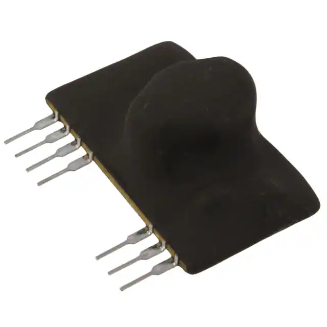
VLA106-24242
Powerex, Inc., 173 Pavilion Lane, Youngwood, Pennsylvania 15697 (724) 925-7272
www.pwrx.com
Isolated
DC/DC Converter
A
B
24242
XXXX
J
L
K
G
+VIN
8
E
H
D
1
11
G
FILTER
F
C
3 +VO1
FILTER
9
3.3kΩ
CONSTANT
VOLTAGE
CIRCUIT
2 +VO2
VZ =
8.2V
1 -VO
DRIVE
CIRCUIT
OVER-CURRENT
PROTECTION
–VIN
10
11
OPTOCOUPLER
Test Circuit Diagram
VIN
C1
+
IO
3
8
9
VLA106-24242
C2
2
10
11
C1 : 100µF 50V (low impedance)
C2 : 47µF 50V (low impedance)
Outline Drawing and Circuit Diagram
Dimensions Inches Millimeters
A
1.3
33.0
B
0.945
24.0
C
0.71
18.0
D
1.0
25.4
E
0.22
5.5
F
0.53
13.5
G
0.18
4.5
H
0.10
2.54
J
0.18±0.06 4.5±1.5
K 0.02+0.004/-0.002 0.5+0.1/-0.05
L 0.01+0.01/-0.002 0.25+0.2/-0.05
+
V
V
1
A
LOAD
Description:
VLA106-24242 is a DC-DC
converter. Its output power is
2.4W and the input is isolated
from the output. The over-current
protection circuit is built-in. This
device is used for on-board power
supplies in industrial control
equipment.
Features:
£ Input Voltage Range:
21.6 to 26.4V DC
£ Output: +24V, 100mA
(Output Power: 2.4W)
£ Thin Profile, Lightweight Design
£ Electrical Isolation Voltage
Between Input and Output:
2500 Vrms for 1 Minute
£ Built in Over-current Protection
Circuit
Application:
On-board power supplies such as
industrial equipment and control
equipment.
Note: All dimensions listed are maximums except D.
7/12 Rev. 1
1
�Powerex, Inc., 173 Pavilion Lane, Youngwood, Pennsylvania 15697 (724) 925-7272 www.pwrx.com
VLA106-24242
Isolated DC/DC Converter
Absolute Maximum Ratings, Ta = 25°C unless otherwise specified
Characteristics
Symbol VLA106-24242 Units
Input Voltage (Between Pins 8, 9, and 10, 11)
VIN
Output Current (Between Pins 3 and 1)
IO 100 mA
27 Volts
Operating Temperature (No Condensation)*
Topr
-20 ~ 70
°C
Storage Temperature (No Condensation)
Tstg
-20 to 85
°C
Input-Output Isolation Voltage (AC, 1 Minute)
VISO 2500 Vrms
*Please refer to derating characteristics.
Electrical and Mechanical Characteristics, Ta = 25°C, VIN = 24V unless otherwise specified
Characteristics
Symbol
Test Conditions
Min.
Typ.
Max.
Units
Input Voltage
VIN
Recommended Range
21.6
24.0
26.4
Volts
Output Voltage 1
VO1
Between Pins 3 and 1, IO = 0 ~ 100mA
22.8
24.0
25.2
Volts
Output Voltage 2
VO2
Between Pins 2 and 1,
7.79
8.2
8.61
Volts
—
—
50
mV
—
50
mV
Between Pins 3 and 2 : No Load
Input Regulation
Reg-I
Between Pins 3 and 1,
IO = 100mA, VIN = 21.6 ~ 26.4V
Load Regulation
Reg-L
Between Pins 3 and 1, IO = 0 ~ 100mA
—
Ripple Voltage
VP-P
Between Pins 3 and 1, IO = 100mA
—
—
150
mV
h
Between Pins 3 and 1, IO = 100mA
—
72
—
%
Efficiency
EFFICIENCY VS. OUTPUT CURRENT
CHARACTERISTICS
EFFICIENCY VS. INPUT VOLTAGE
CHARACTERISTICS
100
100
VIN = 24V
Ta = 25°C
60
40
OUTPUT VOLTAGE, VO, (VOLTS)
80
60
40
20
20
0
30
60
90
120
150
0
180
21
22
23
24
25
26
8
0 20 40 60 80 100 120 140 160 180
OUTPUT VOLTAGE VS. INPUT VOLTAGE
CHARACTERISTICS
INPUT CURRENT VS. INPUT VOLTAGE
CHARACTERISTICS
DERATING
CHARACTERISTICS
140
Io = 100mA
Ta = 25°C
INPUT CURRENT, IIN, (mA)
20
16
12
8
120
OUTPUT CURRENT, IO, (mA)
400
300
200
100
5
10
15
20
INPUT VOLTAGE, VIN, (VOLTS)
25
30
0
100
80
60
40
20
4
2
12
0
27
500
0
16
OUTPUT CURRENT, IO, (mA)
24
0
20
4
Io = 100mA
Ta = 25°C
20
24
INPUT VOLTAGE, VIN, (VOLTS)
Io = 100mA
Ta = 25°C
28
VIN = 24V
Ta = 25°C
OUTPUT CURRENT, IO, (mA)
32
OUTPUT VOLTAGE, VO, (VOLTS)
32
28
EFFICIENCY, h, (%)
EFFICIENCY, h, (%)
80
0
OUTPUT VOLTAGE VS. OUTPUT CURRENT
CHARACTERISTICS
0
5
10
15
20
INPUT VOLTAGE, VIN, (VOLTS)
25
30
0
-10
10
30
50
70
90
110
AMBIENT TEMPERATURE, (°C)
7/12 Rev. 1
�
