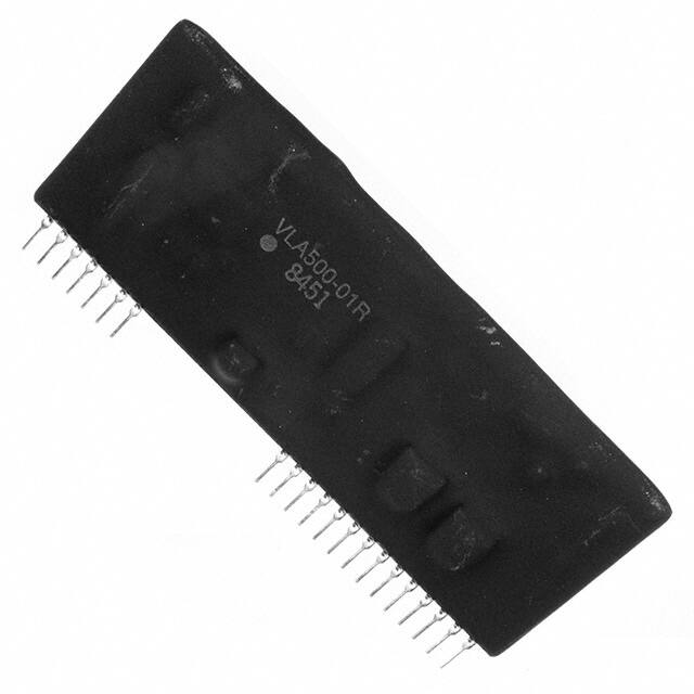
VLA500-01
Powerex, Inc., 200 E. Hillis Street, Youngwood, Pennsylvania 15697-1800 (724) 925-7272
A
Hybrid IC
IGBT Gate Driver +
DC/DC Converter
C
B
D
E
F
D
G
30
1
REGULATOR
16.4 VDC
1
+
19 VCC
2
DC-DC
CONVERTER
Viso =
2500VRMS
VD
15V
–
20 GND
27 SHUTDOWN
SPEED ADJUST
FAULT
LATCH
AND TIMER
3
4
28 FAULT
VGE
DETECTOR
29 ttrip ADJUST
30 VCE DETECT
25
+
CONTROL
INPUT
5V
–
26
6
INTERFACE
BUFFER
7
180Ω
23
24 VO
21
OPTO COUPLER
22 VEE
Outline Drawing and Circuit Diagram
Dimensions
A
B
C
D
E
F
G
Inches
3.27
1.3
0.61
0.2
0.1
0.45
0.18
Millimeters
83.0
33.0
15.5
5.0
2.54
11.5
4.5
Description:
VLA500-01 is a hybrid integrated
circuit designed for driving IGBT
modules. This device is a fully
isolated gate drive circuit consisting of an optimally isolated gate
drive amplifier and an isolated
DC-to-DC converter. The gate
driver provides an over-current
protection function based on
desaturation detection.
Features:
£ Built-in Isolated DC-to-DC
Converter for Gate Drive
£ SIP Outline Allows More Space
on Mounting Area
£ Built-in Short-Circuit Protection
(With Fault Output)
£ Variable Fall Time on Short Circuit Protection
£ Electrical Isolation Voltage
Between Input and Output
(2500 Vrms for 1 Minute)
£ TTL Compatible Input
Application:
To drive IGBT modules for inverter
or AC servo systems applications
Recommended IGBT Modules:
600V module up to 600A
1200V module up to 1400A
Note: All dimensions listed are maximums except E.
Rev. 2/08
1
�Powerex, Inc., 200 E. Hillis Street, Youngwood, Pennsylvania 15697-1800 (724) 925-7272
VLA500-01
Hybrid IC IGBT Gate Driver +
DC/DC Converter
Absolute Maximum Ratings, Ta = 25°C unless otherwise specified
Characteristics
Symbol
VLA500-01
Units
VD
-1 ~ 16.5
Volts
Input Signal Voltage (Applied between Pin 6 - 7, 50% Duty Cycle, Pulse Width 1ms)
Vi
-1 ~ 7
Volts
Output Voltage (When the Output Voltage is "H")
VO
VCC
Volts
Output Current
IOHP
-12
Amperes
(Pulse Width 2µs)
IOLP
12
Amperes
Isolation Voltage (Sine Wave Voltage 60HZ, for 1 Minute)
VISO
2500
Vrms
Case Temperature1 (Surface Temperature Opto-coupler Location)***
TC1
85
°C
Supply Voltage, DC
Case Temperature2 (Surface Temperature Except Opto-coupler Location)
TC2
100
°C
Operating Temperature (No Condensation Allowable)
Topr
-20 to 60
°C
Storage Temperature (No Condensation Allowable)
Tstg
-25 to 100*
°C
Fault Output Current (Applied Pin 28)
IFO
20
mA
Input Voltage to Pin 30 (Applied Pin 30)
VR30
50
Volts
Gate Drive Current (Average)
Idrive
210**
mA
*Differs from temperature cycle condition.
**Refer to Idrive VS. Ta CHARACTERISTICS (TYPICAL) graph. (Needs Derating)
***TC1 Measurement Point (opto-coupler location)
MARKING SIDE
TC1 MEASUREMENT POINT
(OPTO-COUPLER LOCATION)
Electrical and Mechanical Characteristics, Ta = 25°C unless otherwise specified, VD = 15V, RG = 2.2 W)
Characteristics
Symbol
Test Conditions
Min.
Typ.
Max.
Units
Supply Voltage
VD
Recommended Range
14.2
15
15.8
Volts
Pull-up Voltage on Input Side
VIN
Recommended Range
4.75
5
5.25
Volts
"H" Input Current
IIH
Recommended Range
15.2
16
19
mA
f
Recommended Range
—
—
20
kHz
Gate Resistance
RG
Recommended Range
1
—
—
W
"H" Input Current
IIH
VIN = 5V
—
16
—
mA
Switching Frequency
Gate Positive Supply Voltage
VCC
—
15.2
—
17.5
Volts
Gate Negative Supply Voltage
VEE
—
-6
—
-11.5
Volts
Gate Supply Efficiency
Eta
Load Current = 210mA
60
75
—
%
Eta = (VCC + |VEE|) x 0.21 / (15 x ID) x 100
"H" Output Voltage
VOH
10kW Connected Between Pin 23-20
14
15.3
16.5
Volts
"L" Output Voltage
VOL
10kW Connected Between Pin 23-20
-5.5
—
-11
Volts
"L-H" Propagation Time
tPLH
IIH = 16mA
0.3
0.6
1
µs
tr
IIH = 16mA
—
0.3
1
µs
tPHL
IIH = 16mA
0.6
1
1.3
µs
tf
IIH = 16mA
—
0.3
1
µs
"L-H" Rise Time
"H-L" Propagation Time
"H-L" Fall Time
2
Rev. 2/08
�Powerex, Inc., 200 E. Hillis Street, Youngwood, Pennsylvania 15697-1800 (724) 925-7272
VLA500-01
Hybrid IC IGBT Gate Driver +
DC/DC Converter
Electrical and Mechanical Characteristics, Ta = 25°C unless otherwise specified, VD = 15V, RG = 2.2 W)
Characteristics
Symbol
Timer
ttimer
Test Conditions
Min.
Typ.
Max.
Units
1
—
2
ms
Between Start and Cancel
(Under Input Sign "L")
Fault Output Current
IFO
Applied Pin 28, R = 4.7kW
—
5
—
mA
Controlled Time Detect Short-Circuit 1
ttrip1
Pin 30 : 15V and More, Pin 29 : Open
—
2.8
—
µs
Controlled Time Detect Short-Circuit 2*
ttrip2
Pin 30 : 15V and More, Pin 29-21, 22 : 10pF
—
3.2
—
µs
15
—
—
Volts
(Connective Capacitance)
SC Detect Voltage
VSC
Collector Voltage of Module
*Length of wiring from Ctrip to Pins 21, 22, and 29 must be less than 5cm.
24
VD = 15V
Ta = 25C
45
40
20
35
30
t2
25
20
15
VCC
14
t1
12
0
|VEE|
8
6
-20
100 200 300 400 500 600 700 800
0
CONNECTIVE CAPACITANCE, Ctrip, (pF) (Pin: 27 – 21)
1.2
VD = 15V
RG = 2.2 W
VIN = 5.0V
Load: CM1400DU-24NF
1.0
tPHL
0.8
0.6
tPLH
0.4
0.2
0
-20
0
20
40
60
AMBIENT TEMPERATURE, T a, (°C)
Rev. 2/08
80
60
8
4
80
1.4
1.2
5.5
tPHL
0.8
0.6
tPLH
0.4
0.2
0
3.5
Ta = 25°C
DC Load
0
0.05
0.10
0.15
0.20
0.25
ttrip VS. T a CHARACTERISTICS
(TYPICAL)
6.0
VD = 15V
RG = 2.2 W
Ta = 25°C
Load: CM1400DU-24NF
1.0
VD =
15V
VD = 14.2V
LOAD CURRENT, IO, (AMPERES) (Pin: 19 – 21, 22)
tPLH, tPHL VS. V I CHARACTERISTICS
(TYPICAL)
1.6
PROPAGATION DELAY TIME “L-H”, t PLH, (µs)
PROPAGATION DELAY TIME “H-L”, t PHL, (µs)
PROPAGATION DELAY TIME “L-H”, t PLH, (µs)
PROPAGATION DELAY TIME “H-L”, t PHL, (µs)
1.4
40
VD = 15.8V
10
AMBIENT TEMPERATURE, T a, (°C)
tPLH, tPHL VS. T a CHARACTERISTICS
(TYPICAL)
1.6
20
12
6
CONTROLLED TIME DETECT
SHORT-CIRCUIT, ttrip1, ttrip2, (µs)
5
VD =
15V
VD = 14.2V
14
10
10
0
VD = 15.8V
16
18
16
VCC, |VEE| VS. IO CHARACTERISTICS
(TYPICAL)
18
VD = 15V
RG = 2.2 W
Load: CM1400DU-24NF
f = 10KHz D.F. = 50%
22
VCC, |VEE|, (VOLTS)
FALL TIME ON ACTIVITY OF
SHORT-CIRCUIT PROTECTION, t1, t2, (µs)
50
VCC, |VEE| VS. T a CHARACTERISTICS
(TYPICAL)
VCC, |VEE|, (VOLTS)
t1, t2 VS. Cs CHARACTERISTICS
(TYPICAL)
5.0
VD = 15V
RG = 2.2 W
Load: CM1400DU-24NF
4.5
4.0
3.5
ttrip2 (Ctrip = 10pF)
3.0
ttrip1 (Ctrip = 0pF)
2.5
2.0
1.5
4.0
4.5
5.0
5.5
INPUT SIGNAL VOLTAGE, V I, (VOLTS)
6.0
1.0
-20
0
20
40
60
80
AMBIENT TEMPERATURE, T a, (°C)
3
�Powerex, Inc., 200 E. Hillis Street, Youngwood, Pennsylvania 15697-1800 (724) 925-7272
VLA500-01
Hybrid IC IGBT Gate Driver +
DC/DC Converter
VD = 15V
Ta = 25°C
INPUT CURRENT, ID, (AMPERES)
7
6
5
4
3
2
1
0
0
25
50
75
100
0.3
0.2
0.1
CONNECTIVE CAPACITANCE, Ctrip, (pF) (Pin: 29 – 21)
20
VD = 15V
Ta = 25°C
70
18
VCC, |VEE|, (VOLTS)
EFFICIENCY, Eta, (%)
50
40
30
20
EFFICIENCY, Eta, (%)
0.20
0
0.05
0.10
0.15
0.20
0.25
VOH
14
12
10
|VOL|
8
6
Ta = 25°C
VCC
14
12
10
|VEE|
8
6
0
14.0 14.5 15.0 15.5 16.0 16.5 17.0
SUPPLY VOLTAGE, VD, (VOLTS)
0
20
40
60
80
AMBIENT TEMPERATURE, Ta, (°C)
VCC, |VEE| VS. VD CHARACTERISTICS
(TYPICAL)
Eta, VS. VD CHARACTERISTICS
(TYPICAL)
IO = 0.1A
Ta = 25°C
16
4
-20
0.25
2
GATE DRIVE CURRENT, Idrive, (AMPERES)
70
0.15
4
10
75
0.10
16
60
0
0.05
18
LOAD CURRENT, IO, (AMPERES) (Pin: 19 – 21, 22)
Eta VS. Idrive CHARACTERISTICS
(TYPICAL)
80
0
VD = 15V
RG = 2.2 W
Load: CM1400DU-24NF
20
0.4
0
125
VD = 15V
Ta = 25°C
0.5
VOH, |VOL| VS. Ta CHARACTERISTICS
(TYPICAL)
22
Ta VS. Idrive CHARACTERISTICS
(TYPICAL)
0.25
GATE DRIVE CURRENT, Idrive, (AMPERES)
CONTROLLED TIME DETECT
SHORT-CIRCUIT, ttrip, (µs)
8
ID VS. IO CHARACTERISTICS
(TYPICAL)
0.6
“H” OUTPUT VOLTAGE, VOH, (VOLTS)
“L” OUTPUT VOLTAGE, |VOL|, (VOLTS)
ttrip VS. Ctrip CHARACTERISTICS
(TYPICAL)
9
0.20
VD =
15V
VD = 16.5V
0.15
0.10
0.05
RG = 1.1 W
Load: CM1400DU-24NF
0
0
20
40
60
80
AMBIENT TEMPERATURE, Ta, (°C)
SWITCHING TIME DEFINITIONS
VIN
(PIN 6 TO 7)
65
tr
tf
60
90%
55
50%
50
VO
45
10%
(PIN 23 TO 22)
40
14.0 14.5 15.0 15.5 16.0
tPLH
tPHL
16.5 17.0
SUPPLY VOLTAGE, VD, (VOLTS)
4
Rev. 2/08
�Powerex, Inc., 200 E. Hillis Street, Youngwood, Pennsylvania 15697-1800 (724) 925-7272
VLA500-01
Hybrid IC IGBT Gate Driver +
DC/DC Converter
Application Circuit
VLA500-01
1
2
3
4
5
6
7
17 18 19 20 21 22 23 24 25 26 27 28 29 30
D1
R2
+15V
OP1
R4
+5V
Fault
CS
C1
Common
Control
DZ1
+
C4
B1
R3
R1
+
C2
+
C3
Ctrip
RG
G
DZ2
DZ3
E
IGBT MODULE
Component Selection:
Design
D1
DZ1
DZ2, DZ3
C1
C2, C3
C4
CS
Ctrip
R1
R2
R3
R4
OP1
B1
Typical Value
0.5A
30V, 0.5W
18V, 1.0W
150µF, 35V
100-1000µF, 35V
0.01µF
0-1000pF
0-200pF
4.7kΩ, 0.25W
3.3kΩ, 0.25W
1kΩ, 0.25W
4.7kΩ, 0.25W
NEC PS2501
CMOS Buffer
Description
VCE detection diode – fast recovery, Vrrm > VCES of IGBT being used (Note 1)
Detect input pin surge voltage protection (Note 2)
Gate surge voltage protection
VD supply decoupling – Electrolytic, long life, low Impedance, 105°C (Note 3)
DC/DC output filter – Electrolytic, long life, low Impedance, 105°C (Note 3,4)
Fault feedback signal noise filter
Adjust soft shutdown – Multilayer ceramic or film (see application note)
Adjust trip time – Multilayer ceramic or film (see application note)
Fault sink current limiting resistor
Fault signal noise suppression resistor
Fault feedback signal noise filter
Fault feedback signal pull-up
Opto-coupler for fault feedback signal isolation
74HC04 or similar – Must actively pull high to maintain noise immunity
Notes:
(1) The VCE detection diode should have a blocking voltage rating equal to or greater than the VCES of the IGBT
being driven. Recovery time should be less than 200ns to prevent application of high voltage to Pin 30.
(2) DZ1 is necessary to protect Pin 30 of the driver from voltage surges during the recovery of D1.
(3) Power supply input and output decoupling capacitors should be connected as close as possible to the pins of the gate driver.
(4) DC-to-DC converter output decoupling capacitors must be sized to have appropriate ESR and ripple current
capability for the IGBT being driven.
Rev. 2/08
5
�Powerex, Inc., 200 E. Hillis Street, Youngwood, Pennsylvania 15697-1800 (724) 925-7272
VLA500-01
Hybrid IC IGBT Gate Driver +
DC/DC Converter
General Description
The VLA500-01 is a hybrid integrated circuit designed to
provide gate drive for high power IGBT modules. This
circuit has been optimized for use with Powerex NFSeries and A-Series IGBT modules. However, the
output characteristics are compatible with most MOS
gated power devices. The VLA500-01 features a compact single-in-line package design. The upright mounting minimizes required printed circuit board space to
allow efficient and flexible layout. The VLA500-01
converts logic level control signals into fully isolated
+15V/-8V gate drive with up to12A of peak drive current.
Isolated drive power is provided by a built in DC-to-DC
converter and control signal isolation is provided by an
integrated high speed opto-coupler. Short circuit protection is provided by means of destauration detection.
Short Circuit Protection
Figure 1 shows a block diagram of a typical desaturation detector. In this circuit, a high voltage fast recovery
diode (D1) is connected to the IGBT’s collector to monitor the collector to emitter voltage. When the IGBT is in
the off state, VCE is high and D1 is reverse biased. With
D1 off the (+) input of the comparator is pulled up to
the positive gate drive power supply (V+) which is normally +15V. When the IGBT turns on, the comparators
(+) input is pulled down by D1 to the IGBT’s VCE(sat).
The (-) input of the comparator is supplied with a fixed
voltage (Vtrip). During a normal on-state condition the
comparator’s (+) input will be less than Vtrip and it’s output will be low. During a normal off-state condition the
comparator’s (+) input will be larger than Vtrip and it’s output will be high. If the IGBT turns on into a short circuit,
the high current will cause the IGBT’s collector-emitter
voltage to rise above Vtrip even though the gate of the
IGBT is being driven on. This abnormal presence of
high VCE when the IGBT is supposed to be on is often
called desaturation. Desaturation can be detected by
a logical AND of the driver’s input signal and the comparator output. When the output of the AND goes high
a short circuit is indicated. The output of the AND can
be used to command the IGBT to shut down in order
to protect it from the short circuit. A delay (ttrip) must be
provided after the comparator output to allow for the normal turn on time of the IGBT. The ttrip delay is set so
that the IGBT's VCE has enough time to fall below Vtrip
during normal turn on switching. If ttrip is set too short,
erroneous desaturation detection will occur. The maxi-
6
mum allowable ttrip delay is limited by the IGBT’s short
circuit withstanding capability. In typical applications
using Powerex IGBT modules the recommended limit is
10µs.
Operation of the VLA500-01 Desaturation Detector
The Powerex VLA500-01 incorporates short circuit
protection using desaturation detection as described
above. A flow chart for the logical operation of the shortcircuit protection is shown in Figure 2. When a desaturation is detected the hybrid gate driver performs a soft
shutdown of the IGBT and starts a timed (ttimer) 1.5ms
lock out. The soft turn-off helps to limit the transient
voltage that may be generated while interrupting the
large short circuit current flowing in the IGBT. During the
lock out the driver pulls Pin 28 low to indicate the fault
status. Normal operation of the driver will resume after
the lock-out time has expired and the control input signal
returns to its off state.
Adjustment of Trip Time
The VLA500-01 has a default short-circuit detection
time delay (ttrip) of approximately 3µs. This will prevent
erroneous detection of short-circuit conditions as long
as the series gate resistance (RG) is near the minimum recommended value for the module being used.
The 3µs delay is appropriate for most applications so
adjustment will not be necessary. However, in some low
frequency applications it may be desirable to use a
larger series gate resistor to slow the switching of
the IGBT, reduce noise, and limit turn-off transient
V+
D1
+
DELAY
ttrip
COMPARE
Vtrip
C
AND
IGBT
MODULE
SHUTDOWN
INPUT
GATE
DRIVE
RG
G
E
E
Figure 1. Desaturation Detector
Rev. 2/08
�Powerex, Inc., 200 E. Hillis Street, Youngwood, Pennsylvania 15697-1800 (724) 925-7272
VLA500-01
Hybrid IC IGBT Gate Driver +
DC/DC Converter
START
IS
VCE > VSC
NO
YES
IS
INPUT
SIGNAL
ON
NO
YES
DELAY
ttrip
voltages. When RG is increased, the switching delay
time of the IGBT will also increase. If the delay becomes long enough so that the voltage on the detect Pin
30 is greater than VSC at the end of the ttrip delay the
driver will erroneously indicate that a short circuit has
occurred. To avoid this condition the VLA500-01 has
provisions for extending the ttrip delay by connecting a
capacitor (Ctrip) between Pin 29 and VEE (Pins 21 and
22). A curve showing the effect of adding Ctrip on time
is given in the characteristic data section of this data
sheet. The waveform defining trip time (ttrip) is shown
in Figure 3. If ttrip is extended care must be exercised
not to exceed the short-circuit withstanding capability
of the IGBT module. Normally this will be satisfied for
Powerex NF and A-Series IGBT modules as long as the
total shut-down time does not exceed 10µs.
Adjustment of Soft Shutdown Speed
YES
IS
VCE > VSC
NO
YES
SLOW SHUTDOWN
DISABLE OUTPUT
SET FAULT SIGNAL
WAIT ttimer
YES
IS
INPUT
SIGNAL
OFF
NO
As noted above the VLA500-01 provides a soft turn-off
when a short circuit is detected in order to help limit the
transient voltage surge that occurs when large short
circuit currents are interrupted. The default shutdown
speed will work for most applications so adjustment is
usually not necessary. In this case CS can be omitted.
In some applications using large modules or parallel
connected devices it may be helpful to make the shutdown even softer. This can be accomplished by
connecting a capacitor (CS) at Pin 27. A curve showing
the effect of CS on short circuit fall time (t1, t2) is given
in the characteristic data section of this data sheet. The
waveform defining the fall time characteristics is shown
in Figure 3.
ttimer
FAULT SIGNAL
(PIN 28)
10V
10V
ttrip
YES
CLEAR FAULT
SIGNAL
ENABLE OUTPUT
SHORT CIRCUIT
PROTECTION
TIMING
DIAGRAM
(PIN 30 OPEN)
t1
t2
90%
50%
-5V
Figure 2. VLA500-01 Desaturation Detector
VO
(PIN 23)
10%
Figure 3. Adjustment of ttrip and Slow Shutdown Speed
Rev. 2/08
7
�


 工商网监
湘ICP备2023018690号
工商网监
湘ICP备2023018690号