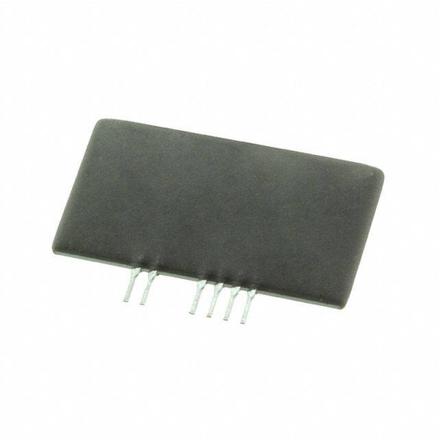
VLA513-01
Powerex, Inc., 200 E. Hillis Street, Youngwood, Pennsylvania 15697-1800 (724) 925-7272
A
Hybrid IC
IGBT Gate Driver
C
B
L
J
K
G
E
D
H
1
D
F
8
6
VCC
2
INTERFACE
1
7
VO
8
VEE
180Ω
OPTO COUPLER
5 PIN: NC
Outline Drawing and Circuit Diagram
Dimensions
A
B
C
D
E
F
G
H
J
K
L
Rev. 04/07
Inches
1.85 Max.
1.063 Max.
0.28 Max.
0.59 Max.
0.10
0.216 Max.
0.08 Max.
0.70
0.18±0.06
0.03
0.02
Millimeters
47.0 Max.
27.0 Max.
7.0 Max.
15.0 Max.
2.54
5.5 Max.
2.0 Max.
17.78
4.5±1.5
0.75
0.5
Description:
VLA513-01 is a hybrid integrated
circuit designed for driving IGBT
modules. This device operates as
an isolation amplifier for these
modules and provides the required
electrical isolation between the
input and output with an optocoupler.
Features:
£ Propagation Delay time:
0.2 µs (Typical)
£ Output is ±5A maximum
£ Two Supply Drive
(VCC: 15 Volts, VEE: -10 Volts)
£ SIP Outline Allows More Space
on Mounting Area
£ Electrical Isolation Voltage
Between Input and Output
(2500 Vrms for 1 Minute)
£ TTL Compatible Input
Application:
To drive IGBT modules for welding,
induction heating, or inverters.
Recommended IGBT Modules:
NFH Series IGBTs –
VCES = 600V & 1200V up to
200A class (f: up to 60kHz),
400A class (f: up to 30kHz)
NF Series IGBTs –
VCES = 600V up to 600A
VCES = 1200V up to 400A
�
�Powerex, Inc., 200 E. Hillis Street, Youngwood, Pennsylvania 15697-1800 (724) 925-7272
VLA513-01
Hybrid IC IGBT Gate Driver
Absolute Maximum Ratings, Ta = 25°C unless otherwise specified
Characteristics
Symbol
VLA513-01
Units
Supply Voltage, DC
VCC
18
Volts
VEE
-12
Volts
VI
-1 ~ 7
Volts
VO
VCC
Volts
IOHP
-5
Amperes
Input Signal Voltage (Applied between Pin 1 - 2, 50% Duty Cycle, Pulse Width 1ms)
Output Voltage (When the Output Voltage is "H")
Output Current
(Pulse Width 2µs, f ≤ 20kHz)
IOLP
5
Amperes
Isolation Voltage (Sine Wave Voltage 60HZ, for 1 Minute)
VISO
2500
Vrms
Case Temperature1 (Surface Temperature Opto-coupler Location)***
TC1
85
°C
Operating Temperature (No Condensation Allowable)
Topr
-20 to 70
°C
Storage Temperature (No Condensation Allowable)
Tstg
-25 to 100*
°C
*Differs from temperature cycle condition.
Electrical and Mechanical Characteristics, Ta = 25°C unless otherwise specified, VCC = 15V, VEE = -10V
Characteristics
Symbol
Supply Voltage
VCC
Recommended Range
Min.
Typ.
Max.
Units
14
15
—
Volts
VEE
Pull-up Voltage on Input Side
VIN
Recommended Range
-5
-8
-12
Volts
Recommended Range
4.75
5
5.25
Volts
"H" Input Current
IIH
Recommended Range
9.5
10.0
14.0
mA
f
Recommended Range
—
—
60
kHz
Gate Resistance
RG
Recommended Range
"H" Input Current
IIH
Switching Frequency
VIN = 5V
—
—
W
10
—
mA
VOH
—
13
14
—
Volts
"L" Output Voltage
VOL
—
-8
-9
—
Volts
"L-H" Propagation Time
tPLH
IIH = 16mA
0.1
0.2
0.5
µs
tr
IIH = 16mA
—
0.3
1
µs
tPHL
IIH = 16mA
0.05
0.2
0.5
µs
tf
IIH = 16mA
—
0.3
1
µs
"H-L" Propagation Time
"H-L" Fall Time
2
—
"H" Output Voltage
"L-H" Rise Time
�
Test Conditions
Rev. 04/07
�Powerex, Inc., 200 E. Hillis Street, Youngwood, Pennsylvania 15697-1800 (724) 925-7272
VLA513-01
Hybrid IC IGBT Gate Driver
0.5
PROPAGATION DELAY TIME “L-H”, tPLH, (µs)
PROPAGATION DELAY TIME “H-L”, tPHL, (µs)
PROPAGATION DELAY TIME “L-H”, tPLH, (µs)
PROPAGATION DELAY TIME “H-L”, tPHL, (µs)
VCC = 15V
VEE = -10V
RG = 3W
VIN = 5V
Load: CM400DU-24NFH
0.6
0.4
0.3
tPLH
0.2
tPHL
0.1
0
0
20
40
60
tPLH, tPHL VS. VI CHARACTERISTICS
(TYPICAL)
0.7
80
VCC = 15V
VEE = -10V
RG = 3W
Ta = 25°C
Load: CM400DU-24NFH
0.6
0.5
0.4
0.3
tPLH
0.2
tPHL
0.1
0
3
AMBIENT TEMPERATURE, Ta, (°C)
18
5
6
7
INPUT SIGNAL VOLTAGE, VI, (VOLTS)
RG = 2W OR MORE*
4
3
2
1
0
0
20
40
60
80
100
AMBIENT TEMPERATURE, Ta, (°C)
ICC VS. (VCC + |VEE|) CHARACTERISTICS
(TYPICAL)
* The following numberical expression must be satisfied
PT > (VCC + IVEEI) * {(Q1 + IQ2I) * f + ICC}
Q1: Gate Charge on plus bias
Q2: Gate Charge on minus bias
f: Switching frequency
ICC: Constant dissipation current of driver
Ta = 25°C
DISSIPATION CURRENT, ICC, (mA)
4
PT VS. Ta
(MAXIMUM RATING)
5
TOTAL POWER DISSIPATION, PT, (WATTS)
tPLH, tPHL VS. Ta CHARACTERISTICS
(TYPICAL)
0.7
15
12
Refer to “ICC VS. (VCC + IVEEI) Characteristics”
9
6
3
0
0
5
10
15
20
25
30
35
SUPPLY VOLTAGE, (VCC + IVEEI), (VOLTS)
Application Circuit
Switching Time Definitions
SWITCHING TIME DEFINITIONS
VI
VLA513-01
VIN
5V
1
2
5
6
7
VO
8
+
tr
tf
90%
CM200DU-24NFH
220µF
RG
+
220µF
VCC
VCC = 15V
VEE = -10V
RG = 3Ω
50%
10%
VEE
Notes:
tPLH
tPHL
(1) Power supply decoupling capacitors should be connected as close as possible
to the pins of the gate driver.
(2) Power supply decoupling capacitors should be good quality, low ESR types.
(3) Printed circuit layout should minimize wiring lengths and utilize shielding layers
to suppress noise.
Rev. 04/07
�
�
