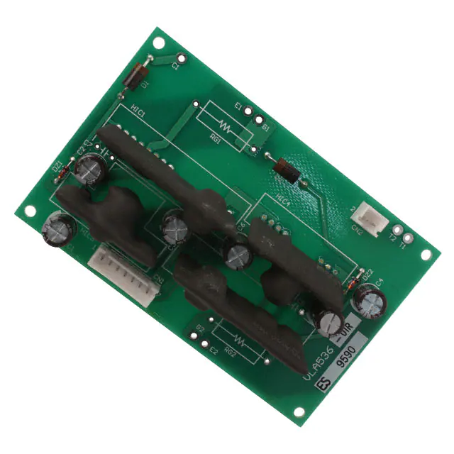
VLA536-01R
Powerex, Inc., 173 Pavilion Lane, Youngwood, Pennsylvania 15697 (724) 925-7272
www.pwrx.com
NX-Series Dual IGBT
Gate Driver
Interface Board
A
D
CONNECTOR
Pin
1
2
3
4
5
6
7
C B
E
CN1
VD
GND
NC
Alarm
IN1
IN2
VIN
CN2
T1
T2
F (4 PLACES)
E
G
J H
Description:
VLA536-01R is a completely
populated gate driver board
designed specifically for
driving NX package style
Powerex IGBT modules rated
up to 600A at 1200V.
BLOCK DIAGRAM
VD
HIC3
+
CONTROL
CIRCUIT
GND
CONSTANT
VOLTAGE
CIRCUIT
+
8.2V
HIC1
Features:
£ Mounts Directly to Dual
NX IGBT Modules
£ Built-in Isolated DC-DC
Converter for Gate Drive
£ Built-in Short Circuit
Protection
£ Electrical Isolation Voltage is
2500 Vrms (for 1 minute)
£ Provides Isolated Control
Power and Gate Drive
£ CMOS Compatible Input
Interface
C1
DETECT
VIN
LATCH
IN1
240 Ω
G1
AMP
TIMER
Alarm
SHUTDOWN FO
E1
HIC4
+
CONTROL
CIRCUIT
CONSTANT
VOLTAGE
CIRCUIT
+
8.2V
HIC2
DETECT
LATCH
IN2
240 Ω
G2
AMP
TIMER
SHUTDOWN FO
E2
T1
T1
T2
T2
Recommended IGBT
Modules:
NX-Series Dual IGBT Modules
600V – Up to 400A
(Example: CM400DX-12A)
Outline Drawing and Circuit Diagram
Dimensions
A
Inches
Dimensions
Inches
Millimeters
3.97±0.04
Millimeters
101.0±1.0
F
0.12 Dia.
3.0 Dia.
B
2.52±0.02
64.0±0.5
G
1.14 Max.
29.0 Max.
C
2.26
57.5
H
0.06
1.6
D
3.75
94.5
J
0.12 Max.
3.0 Max.
E
0.13
04/16 Rev. 2
3.25
1200V – Up to 600A
(Example: CM600DX-24S1)
Application:
To drive IGBT modules for
inverter or AC servo systems
applications
1
�Powerex, Inc., 173 Pavilion Lane, Youngwood, Pennsylvania 15697 (724) 925-7272 www.pwrx.com
VLA536-01R
NX-Series Dual IGBT
Gate Driver Interface Board
Absolute Maximum Ratings, Ta = 25°C unless otherwise specified
Characteristics
Symbol VLA536-01R Units
Supply Voltage (DC)
VD 18 Volts
Input Signal Voltage (Applied between VIN - IN1, IN2, 50% Duty Cycle, Pulse Width 1ms)
VI
-1 ~ +7
Volts
Gate Peak Current
IOHP -5 A
(Pulse Width 2µs)
IOLP 5 A
Operating Temperature (No Condensation)
Topr
-20 ~ +70
°C
Storage Temperature (No Condensation)
Tstg
-25 ~ +85
°C
Alarm Pin Output Sink Current
Ialm 10 mA
Alarm Pin Voltage
Valm 50 Volts
Gate Drive Current (Gate Averge Current Per One Circuit)
Idrive 83 mA
Isolation Voltage (Sine Wave Voltage, 60Hz, 1 Minute)
VISO 2500 Vrms
Electrical and Mechanical Characteristics, Ta = 25°C, VD = 15V unless otherwise noted
Characteristics
Symbol
Test Conditions
Min.
Typ.
Max.
Units
Supply Voltage
VD
Recommended Range
12
15
18
Volts
Input Voltage
VIN
Recommended Range
4.75
5.0
5.25
Volts
Input Signal Current
IIH
Recommended Range
10
13
16
mA
Switching Frequency
f
Recommended Range
–
–
20
kHz
Gate Resistance
RG
Recommended Range
2 –
–
Ω
Alarm Output Current
Ialm
Recommended Range
– –
5
mA
Plus Bias Voltage
VOH
14.5 16
17.5
Volts
Minus Bias Voltage
VOL
-9 -8
-7
Volts
"L-H" Propagation Time
tPLH
IIH = 13mA
0.2
0.45
0.8
µs
"H-L" Propagation time
tPHL
IIH = 13mA
0.2
0.4
0.7
µs
Between Start and Clear
1.0
1.4
2.0
ms
–
6.5
10.0
µs
–
–
Volts
(Pull-up Voltage on Input Side)
Timer
t_timer
(Under Input Signal "OFF")
2
Alarm Delay Time
tdalm
Ialm = 2.5mA
SC Detect Threshold Voltage
VSC
IGBT Collector Voltage
–
04/16 Rev. 2
�Powerex, Inc., 173 Pavilion Lane, Youngwood, Pennsylvania 15697 (724) 925-7272 www.pwrx.com
VLA536-01R
NX-Series Dual IGBT
Gate Driver Interface Board
Inner Circuit
CN1
3
8
9
VD
C3
+
HIC3
GND
10
11
NC
Alarm
4
1
HIC1
16
15
14
13
2
+
1
C2
C1
DZ1
5
+
C1
2
D1
G1
RG1
E1
6
IN1
IN2
3
8
9
+
HIC4
C6
10
11
4
+
C5
D2
SanKen
Low Impedance
TDK FK28 Type
RG1, RG2
CN1
CN2
JST
JST
3W Class
B7B-XH-A
B2B-XH-A
ISAHAYA
ISAHAYA
NOTE:
Gate Resistor is not included. Please install selected resistor.
DZ2
5
+
C4
2
1
1
HIC2
16
15
14
13
2
VIN
Parts List (Reference)
HIC1, HIC2
VLA520-01R
HIC3, HIC4
VLA106-15252
DZ1, DZ2
30V, 500mW
D1, D2
RP1H
C1 ~ 6
100μF, 50V
C7, C8
10pF ~ 50pF, 50V
C7, C8 is not installed at the time of shipment. Please solder in
selected capacitor if needed. (Rough Guide 10 ~ 50pF, 50V, Ceramic)
G2
RG2
E2
6
CN2
T1
T1
T2
T2
Application Example
VLA536-01R
IGBT Module
CN1
5V
15V
4.7kΩ
C3
+
10
11
NC
FO
HIC3
GND
3
8
9
VD
4
1
HIC1
16
15
14
13
2
+
1
C2
C1
DZ1
G1
5
+
C1
2
D1
RG1
E1
6
IN1
INPUT
SIGNAL
RC
FILTER
~10µs
IN2
HC04
ETC.
CN2
T1
T2
+
10
11
HIC4
C6
04/16 Rev. 2
3
8
9
4
+
C4
2
+
1
C5
1
HIC2
16
15
14
13
2
VIN
D2
DZ2
G2
5
RG2
6
E2
T1
T2
3
�Powerex, Inc., 173 Pavilion Lane, Youngwood, Pennsylvania 15697 (724) 925-7272 www.pwrx.com
VLA536-01R
NX-Series Dual IGBT
Gate Driver Interface Board
Short Circuit Detection Flow Diagram
START
DETECTION OF
SHORT CIRCUIT
GATE SHUTDOWN TIMER
START OUTPUT ALARM
1 ~ 2ms
END OF TIMER
NOTE:
If the gate voltage is “H” and the
collector voltage is high, the gate driver
will recognize the circuit as a short
circuit and immediately reduces the gate
voltage (slow shutdown). It will also give
an alarm signal showing that the SC
protection circuit is operating.
The protection circuit resets if input
signal is OFF when the predetermined
time (1 ~ 2ms) has passed. (An OFF
period of more than 40µm is required.)
INPUT SIGNAL
IS OFF
CLEAR ALARM
ENABLE OUTPUT
PCB Installation
SOLDER C / G / E / T PINS
4
04/16 Rev. 2
�
很抱歉,暂时无法提供与“VLA536-01R”相匹配的价格&库存,您可以联系我们找货
免费人工找货