VLA567-01R
Powerex, Inc., 173 Pavilion Lane, Youngwood, Pennsylvania 15697 (724) 925-7272
www.pwrx.com
Hybrid IC
IGBT Gate Driver +
DC/DC Converter
Description:
VLA567-01R is a hybrid
integrated circuit designed for
driving n-channel IGBT modules.
This device includes the isolated
DC-DC converter required for gate
drive.
A
44
23
B
1
D
The built-in short circuit protection
provides gate lockout to maintain
reverse bias for a predetermined
time after the detection of the short
circuit.
E
22
F
H
Features:
£ Low Height, DIP Structure
£ Built-in Isolated DC-DC
Converter for Gate Drive
£ Output Peak Current is
±8A Max.
£ Built-in Short Circuit Protection
£ Electrical Isolation Voltage is
2500 Vrms (for 1 Minute)
£ CMOS Compatible Input
Interface
£ Adjustable Fall Time for Short
Circuit Protection
Recommended IGBT Modules:
VCES = 600V up to 600A
VCES = 1200V up to 600A
G
C
J
25 VCC1
TIMER &
RESET
LATCH
DETECT
VI+1 40
INTERFACE
1kΩ
VI-1 41
28 E1
29 FO1
GATE
SHUTDOWN
TEST2 42
UVL
DC-AC CONVERTER
Gi 43
24 Ctrip1
26 VO1
240Ω
PC
VD 44
23 DETECT 1
30 CS1
27 VEE1
VCC1
31 NC
VEE1
UVL
VCC2
14 NC
VEE2
TEST1 1
20 VCC2
TIMER &
RESET
LATCH
DETECT
VI+2 4
INTERFACE
1kΩ
VI-2 5
22 DETECT 2
21 Ctrip2
19 VO2
17 E2
240Ω
PC
VI-2 2
16 FO2
GATE
SHUTDOWN
15 CS2
18 VEE2
NC 3
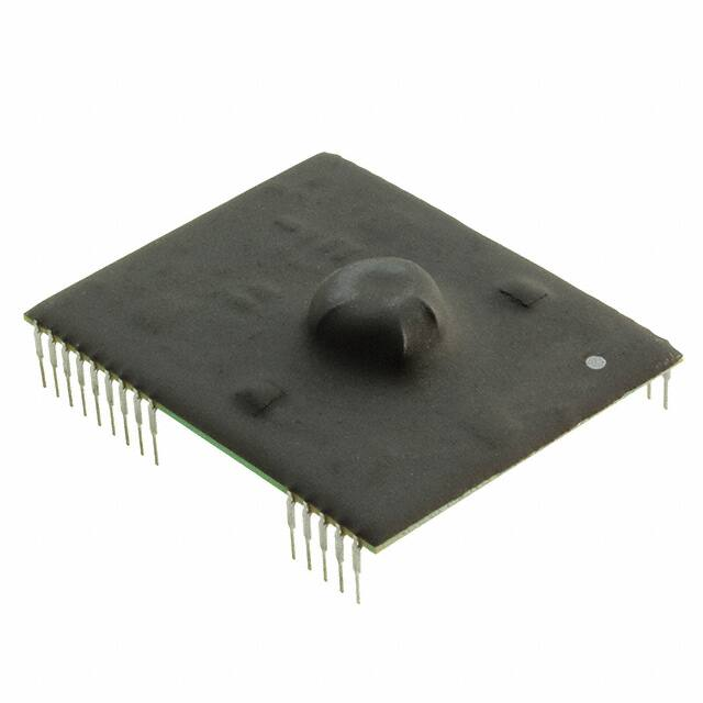
Outline Drawing and Circuit Diagram
Dimensions
Inches
Millimeters
A
2.44 Max.
62.0 Max.
B
1.89 Max.
48.0 Max.
C
0.02±0.0039
0.5±0.1
H
0.14
3.5
D
1.8
45.72
J
0.1
2.54
E
Dimensions
Inches
Millimeters
F
0.67 Max.
17.0 Max.
G
0.177±0.06
4.5±1.5
0.01+0.0067/-0.0039 0.27+0.17/-0.1
05/16 Rev. 2
1
�Powerex, Inc., 173 Pavilion Lane, Youngwood, Pennsylvania 15697 (724) 925-7272 www.pwrx.com
VLA567-01R
Hybrid IC IGBT Gate Driver
+ DC/DC Converter
Absolute Maximum Ratings, Ta = 25°C unless otherwise specified
Characteristics
Symbol Rating Units
Supply Voltage (DC)
VD 16.5 Volts
Input Signal Voltage (Applied Between Vl+ - Vl-, 50% Duty Cycle, Pulse Width 1ms)
Output Peak Current (Pulse Width 2μs)
VI
-1 ~ +7
Volts
IOHP +8 Amperes
IOLP -8 Amperes
Operating Temperature (No Condensation Allowable)
Storage Temperature (No Condensation
Topr
Allowable)*1 T
Fault Output Current (Applied FO-Pin)
Input Voltage at DETECT-pin (Applied DETECT-Pin)
stg
-20 ~ 70
°C
-40 ~ 90
°C
IFO 20 mA
VR-DET 50 Volts
Gate Drive Current (Gate Average Current Per One Circuit)
Idrive 100 mA
Isolation Voltage Between Input and Output (Sine Wave Voltage, 60Hz for 1 Minute)
Viso1 2500 Vrms
Isolation Voltage Between Each Onput (Sine Wave Voltage, 60Hz for 1 Minute)
Viso2 2500 Vrms
*1 Differs from H/C condtion.
2
05/16 Rev. 2
�Powerex, Inc., 173 Pavilion Lane, Youngwood, Pennsylvania 15697 (724) 925-7272 www.pwrx.com
VLA567-01R
Hybrid IC IGBT Gate Driver
+ DC/DC Converter
Electrical Characteristics, Ta = 25°C, VD = 15V, RG = 2Ω unless otherwise specified
Characteristics
Symbol
Test Conditions
Min.
Typ.
Max.
Units
Supply Voltage
VD
Recommended Range
14.2
15.0
15.8
Volts
Pull-up Voltage on Input Side
VIN
Recommended Range, (When VIN = 15V, "H"
4.75
5.00
5.25
Volts
"H" Input Signal Current*3
IIH
Recommended Range
10
13
16
mA
Input Current Must Stay in Recommended Range)
Switching Frequency
f
Recommended Range
—
—
20
kHz
Gate Resistance
RG
Recommended Range
2
—
—
Ω
Gate Positive Supply Voltage
VCC
—
16.8
—
Volts
Gate Negative Supply Voltage
VEE
—
-8.5
—
Volts
η
VD = 15V, Load Current = 100mA x 2
70
79
—
%
VOH
RG = 2Ω, f = 10kHz, Load Current = 0.22μF
13.5
15.5
16.5
Volts
"L" Output Voltage*3
VOL
RG = 2Ω, f = 10kHz, Load Current = 0.22μF
—
-8.0
—
Volts
"L-H" Propagation Time*3
tPLH
IIH = 13mA
0.2
0.4
1
μs
tr
IIH = 13mA
—
0.4
1
μs
tPHL
IIH = 13mA
0.2
0.4
1
μs
Gate Supply Efficiency
"H" Output Voltage*3
"L-H" Rise
Time*3
"H-L" Propagation Time*3
"H-L" Fall
Time*3
tf
IIH = 13mA
—
0.3
1
μs
ttimer
Between Start and Cancel (Under Input Sign "L")
1
—
2
ms
Fault Output Current
IFO
Applied Pin 16, 29*4
—
5
—
mA
Controlled Time Detect Short Circuit 1
ttrip1
Pin 22, 23 : 15V or More, Pin 21, 24 : Open
—
2.4
—
μs
ttrip2
Pin 22, 23 : 15V and More,
—
3.2
—
μs
Timer
Controlled Time Detect Short Circuit
2*2
Pin 17-21, 24-28 : 47pF
SC Detect Voltage
Under Voltage Lock Out
VSC
Collector Voltage of Module
15
—
—
Volts
UVLO_VCC
Voltage of VCC
—
11.5
—
Volts
*2 Length of wiring of condenser controlled time detect short-circuit is within 5cm from Pin 17 and 21 (24 and 28) coming and going.
*3 When LED of PC is ON (luminescence), VO is high.
*4 With pull-up 4.7k ohm.
05/16 Rev. 2
3
�Powerex, Inc., 173 Pavilion Lane, Youngwood, Pennsylvania 15697 (724) 925-7272 www.pwrx.com
VLA567-01R
Hybrid IC IGBT Gate Driver
+ DC/DC Converter
Definition of Characteristics
OPERATION OF SHORT CIRCUIT PROTECTION
SWITCHING OPERATION
VI
VI 0V
tr
VO
tf
VO 0V
90%
-5V
ttrip 1, 2
50%
FO
10%
tPLH
tPHL
ttimer
10V
10V
0V
Application Example
PC1
4.7kΩ
29
P
4.7kΩ
23
GATE SIGNAL 1
40
26
41
25
GND
28
42
44
DZ2,
DZ3
+
C1
HC04 ETC.
D1
RG1
+
C2
IGBT MODULE
VIN : 5V
DZ1
27
VD : 15V
24
Ctrip1
CS1
30
43
1
VLA567-01R
D2
22
RG2
19
4
GATE SIGNAL 2
20
5
HC04 ETC.
17
GND
+
DZ5,
DZ6
C3
+
C4
DZ4
18
Ctrip2
21
4.7kΩ
15
16
N
CS2
4.7kΩ
PC2
NOTE:
1. Low impedance capacitors (C1~C4) should be connected as close as possible to the hybrid IC.
2. D1 requires approximately the same blocking voltage as the power modules.
3. If the reverse recovery time of D1 or D2 is long, Pin 22 or Pin 23 can end up with high voltage. For
additional protection, insert a zener diode between Pin 18 and Pin 22 as well as between Pin 23
and Pin 27 as shown in the application example circuit.
4. If using an external Ctrip capacitor at Pin 21 or Pin 24, the Ctrip must be wired as close as possible
to the IC’s pins (less than 5cm total).
5. The wiring length from the driver’s output to the IGBT’s gate should be kept as short as possible,
as should the signal connections from the controller to the driver’s inputs in order to avoid errors
caused by circuit noise.
6. A 4.7kΩ resistor can be connected between Pins 17 and 22 as well as between Pins 23 and 28 if
short-circuit protection is not desired. In this case D1, D2, DZ1 and DZ4 should be left out and
Pins 16 and 29 should be left unconnected.
7. Pins 1 and 42 are for manufacturing test purposes, and should be left unconnected.
4
VD = 15V ±5%
VIN = 5V ±5%
C1 ~ 4 = 100μF, 50V (Low Impedance)
Ctrip1, Ctrip2 : Depended on RG1, RG2
(Aim : 0 ~ 47pF, 40V, Ceramic)
CS1, CS2 : Depends on Serge Voltage
Z1, Z4 : 30V
DZ2, DZ3, DZ5, DZ6 : 18V
D1, D2 : Fast Recovery Diode (trr : 0.2µs max.) RP1H(Sanken) etc.
PC1, PC2 : TLP781(Toshiba), PS2501 (NEC) etc.
05/16 Rev. 2
�Powerex, Inc., 173 Pavilion Lane, Youngwood, Pennsylvania 15697 (724) 925-7272 www.pwrx.com
VLA567-01R
Hybrid IC IGBT Gate Driver
+ DC/DC Converter
Operation of Protection Circuit
Adjustment of Output Fall Time
1. When an “ON” input signal is applied for a period longer than Ttrip
and the collector voltage is high, the hybrid IC will recognize the
condition as a short-circuit and immediately reduce the gate voltage.
It will also produce a low voltage fault signal at the respective Pin 29
or Pin 16 alerting that the protection circuit is in operation.
2. The protection circuit will reset if an “OFF” input signal is applied and
the minimum 1~2ms shutdown time has passed. “OFF” signal must
be 10μs or more.
3. The controlled time to detect a short-circuit (Ttrip) should be set so
that the IGBT can be fully turned “ON” before a short-circuit condition
can be detected. It is possible to adjust Ttrip by connecting a capacitor (Ctrip) between Pins 17 and 21, as well as Pins 28 and 24.
4. When the short-circuit protection is activated, the soft gate shutdown
circuit reduces the collector surge voltage on the IGBT. The gate shut
down speed can be slowed even more by adding a capacitor to the
CS terminal (between Pins 15 and 18; Pins 27 and 30).
ts
13V
0V
VO
Operation Flow on Detecting Short Circuit
START
ts- CS CHARACTERISTICS
(TYPICAL)
DETECTION OF
SHORT CIRCUIT
GATE SHUTDOWN
CIRCUIT OPERATE
TIMER START
OUTPUT FAULT SIGN
END OF TIMER
1 ~ 2ms
NO
YES
INPUT SIGN
IS “OFF”
FALL TIME ON ACTIVITY OF
SHORT CIRCUIT PROTECTION, ts, (µs)
70
60
50
40
30
20
10
NO
YES
RESET
0
0
100
200 300 400 500 600
CONNECTIVE CAPACITANCE, CS, (pF)
PIN: 15-18 (27 – 30)
NOTE: “L” output voltage (VOL) with protection
circuit operating is about VEE + 2V
05/16 Rev. 2
5
�Powerex, Inc., 173 Pavilion Lane, Youngwood, Pennsylvania 15697 (724) 925-7272 www.pwrx.com
VLA567-01R
Hybrid IC IGBT Gate Driver
+ DC/DC Converter
20
18
18
16
16
14
14
12
10
8
6
2
0
-20
1.0
PROPAGATION DELAY TIME “L-H”, tPLH, (μs)
PROPAGATION DELAY TIME “H-L”, tPHL, (μs)
VCC, | VEE|, (VOLTS)
20
4
0.8
VD = 15V
RG = 2Ω
LOAD : C = 0.22μF
f = 10kHz
0
20
40
60
12
10
8
6
DC LOAD
VD = 15.8V
VD = 15V
VD = 14.2V
4
VCC
| VEE |
2
0
80
0
20
40
60
80
AMBIENT TEMPERATURE, Ta, (°C)
LOAD CURRENT, IO, (AMPERES)
PIN: 18-20 (27-25)
tPLH, tPHL-Ta CHARACTERISTICS
(TYPICAL)
tPLH, tPHL-VI CHARACTERISTICS
(TYPICAL)
0.6
VD = 15V
RG = 2Ω
LOAD : C = 0.22μF
tPLH
tPHL
0.6
0.4
0.2
0
-20
0
20
40
60
AMBIENT TEMPERATURE, Ta, (°C)
6
VCC, | VEE | -IO CHARACTERISTICS
(TYPICAL)
PROPAGATION DELAY TIME “L-H”, tPLH, (μs)
PROPAGATION DELAY TIME “H-L”, tPHL, (μs)
VCC, | VEE|, (VOLTS)
VCC, | VEE | CHARACTERISTICS
(TYPICAL)
80
100
0.5
0.4
0.3
0.2
0.1
0
3.5
VD = 15V
LOAD : C = 0.22μF
tPLH
tPHL
4.0
4.5
5.0
5.5
6.0
INPUT SIGNAL VOLTAGE, VI, (VOLTS)
05/16 Rev. 2
�Powerex, Inc., 173 Pavilion Lane, Youngwood, Pennsylvania 15697 (724) 925-7272 www.pwrx.com
VLA567-01R
Hybrid IC IGBT Gate Driver
+ DC/DC Converter
ttrip-Ta CHARACTERISTICS
(TYPICAL)
5.0
8
VD = 15V
RG = 2Ω
LOAD : C = 0.22μF
4.0
3.5
3.0
2.5
2.0
1.5
1.0
ttrip1 (Ctrip = 0pF)
ttrip2 (Ctrip = 47pF)
0.5
0
-20
0
20
40
60
4
3
2
0
100 150 200 250 300
CONNECTIVE CAPACITANCE, Ctrip, (pF)
PIN: 17-21 (24-28)
ID-IO CHARACTERISTICS
(TYPICAL)
VOH, | VOL | -Ta CHARACTERISTICS
(TYPICAL)
20
0.4
0.3
0.2
0.1
0
50
AMBIENT TEMPERATURE, Ta, (°C)
“H” OUTPUT VOLTAGE, VOH, (VOLTS)
“L” OUTPUT VOLTAGE, | VOL |, (VOLTS)
INPUT CURRENT, ID, (AMPERES)
5
0
80
VD = 15V
DRIVING DOUBLE CIRCUIT
0.5
0.02
0.04
0.06
0.08
LOAD CURRENT, IO, (AMPERES)
PIN: 44, 18-20 (27-25)
05/16 Rev. 2
6
1
0.6
0
VD = 15V
RG = 2Ω
LOAD : C = 0.22μF
7
CONTROLLED TIME DETECT
SHORT CIRCUIT, ttrip, (μs)
4.5
CONTROLLED TIME DETECT
SHORT CIRCUIT, ttrip1, ttrip2, (μs)
ttrip-Ctrip CHARACTERISTICS
(TYPICAL)
0.10
18
16
14
12
10
8
6
4
2
0
-20
VD = 15V
RG = 2Ω
LOAD : C = 0.22μF
f = 10kHz
0
20
VOH
| VOL |
40
60
80
AMBIENT TEMPERATURE, Ta, (°C)
7
�Powerex, Inc., 173 Pavilion Lane, Youngwood, Pennsylvania 15697 (724) 925-7272 www.pwrx.com
VLA567-01R
Hybrid IC IGBT Gate Driver
+ DC/DC Converter
90
20
80
18
70
16
VCC, | VEE |, (VOLTS)
EFFICIENCY, η, (%)
η-Idrive CHARACTERISTICS
(TYPICAL)
60
50
40
30
20
VD = 15V
DRIVING DOUBLE CIRCUIT
0
0.02
0.04
0.06
0.08
10
8
6
0
14.0
0.10
IO = 0.1A
VCC
| VEE |
14.5
15.0
15.5
GATE DRIVE CURRENT, Idrive, (AMPERES)
SUPPLY VOLTAGE, VD, (VOLTS)
DERATING CHARACTERISTICS
(TYPICAL)
η-VD CHARACTERISTICS
(TYPICAL)
90
16.0
0.10
85
0.08
EFFICIENCY, η, (%)
GATE DRIVE CURRENT, Idrive, (AMPERES)
12
2
0.12
0.06
0.04
0.02
0
-20
LOAD : C = 0.22μF
DRIVING DOUBLE CIRCUIT
0
20
80
75
VIN = 15.8V
VIN = 15V
VIN = 14.2V
IO = 0.1A
DRIVING DOUBLE CIRCUIT
40
60
AMBIENT TEMPERATURE, Ta, (°C)
8
14
4
10
0
VCC, | VEE | -VD CHARACTERISTICS
(TYPICAL)
80
70
14.0
14.5
15.0
15.5
16.0
SUPPLY VOLTAGE, VD, (VOLTS)
05/16 Rev. 2
�