1SP0635x2xx-12
1SP0635x2xx-12
Preliminary Data Sheet
Compact, high-performance, plug-and-play single-channel IGBT driver based
on SCALE™-2 technology for individual and parallel-connected modules in
2-level, 3-level and multilevel converter topologies
Abstract
The SCALE™-2 plug-and-play driver 1SP0635x2xx-12 is a compact single-channel intelligent gate driver
designed for 1200V 130x140mm and 190x140mm IGBT modules. The master driver 1SP0635x2Mx-12 features
a fiber-optic interface with a built-in isolated DC/DC power supply. It can be used as stand-alone driver or in
conjunction with up to three 1SP0635D2Sx-12 slaves to drive up to four parallel-connected IGBT modules.
The turn-on and turn-off gate resistors as well as the auxiliary gate capacitor are not assembled
in order to provide maximum flexibility. They must be assembled by the user before start of
operation. Please refer to the paragraph on “Gate Resistor Assembly” for the recommended values.
For drivers adapted to other types of high-power and high-voltage IGBT modules, refer to:
www.IGBT-Driver.com/go/plug-and-play
Features
Applications
Plug-and-play solution
Allows parallel connection of IGBT modules
For 2-level, 3-level and multilevel topologies
Built-in isolated DC/DC power supply (master)
Fiber-optic links (master)
Built-in interface to 1SP0635D2Sx (slave)
Duty cycle 0...100%
Dynamic Advanced Active Clamping DA C
Dynamic IGBT short-circuit protection
Monitoring of supply voltage
Monitoring of gate voltage
Extremely reliable; long service life
Shortens application development time
Suitable for 1200V 130x140mm
2
Traction
Railroad power supplies
Light rail vehicles
HVDC
Flexible AC transmission systems (FACTS)
Medium-voltage converters
Industrial drives
Wind-power converters
Medical applications
Research
And many others
and 190x140mm IGBT modules
www.IGBT-Driver.com
Page 1
�1SP0635x2xx-12
Preliminary Data Sheet
Safety Notice!
The data contained in this data sheet is intended exclusively for technically trained staff. Handling all highvoltage equipment involves risk to life. Strict compliance with the respective safety regulations is mandatory!
Any handling of electronic devices is subject to the general specifications for protecting electrostatic-sensitive
devices according to international standard IEC 60747-1, Chapter IX or European standard EN 100015 (i.e. the
workplace, tools, etc. must comply with these standards). Otherwise, this product may be damaged.
Important Product Documentation
This data sheet contains only product-specific data. For a detailed description, must-read application notes and
common data that apply to the whole series, please refer to the “Description & Application Manual for
1SP0635 SCALE-2 IGBT Drivers” on www.IGBT-Driver.com/go/1SP0635.
The gate resistors as well as the auxiliary gate capacitor on this gate driver are not assembled in order to
provide maximum flexibility. For the values required for specific IGBT modules, refer to the paragraph on
“Gate Resistor Assembly”. Use of gate resistors and gate auxiliary capacitors other than those specified may
result in failure.
Mechanical Dimensions
Dimensions: See the relevant “Description and Application Manual”
Mounting principle: Connected to IGBT module with screws
Fiber-Optic Interfaces (1SP0635x2Mx)
Interface
Remarks
Part type #
Drive signal input
Drive signal input
Status output
Status output
1SP0635V, fiber-optic receiver (Notes 1, 2)
1SP0635S, fiber-optic receiver (Notes 1, 2)
1SP0635V, fiber-optic transmitter (Notes 1, 3)
1SP0635S, fiber-optic transmitter (Notes 1, 3)
HFBR-2522Z
HFBR-2412Z
HFBR-1522Z
HFBR-1412Z
Interface
Remarks
Part type #
Power supply connector X1
Bus connectors X2 and X3
1SP0635x2Mx, on-board connector (Note 4)
On-board connectors (Note 5)
Electrical Connectors
www.IGBT-Driver.com
214012
214013
Page 2
�1SP0635x2xx-12
Preliminary Data Sheet
Absolute Maximum Ratings
Parameter
Remarks
Supply voltage V DC
Average supply current I DC
Average supply current I DC
Gate output power
VDC to GND (1SP0635x2Mx)
1SP0635x2Mx only (Note 6)
1SP0635x2Mx with three 1SP0635D2Sx (Note 6)
1SP0635x2Mx, Ta < 70°C (Note 7)
1SP0635x2Mx, Ta = 85°C (Note 7)
1SP0635D2Sx, Ta < 70°C (Note 8)
1SP0635D2Sx, Ta = 85°C (Note 8)
1SP0635x2Mx, Ta < 70°C (Note 31)
1SP0635x2Mx, Ta = 85°C (Note 31)
1SP0635D2Sx, Ta < 70°C (Note 31)
1SP0635D2Sx, Ta = 85°C (Note 31)
Note 9
1SP0635x2Mx, primary to secondary (Note 10)
Switching operation (Note 11)
Off state (Note 12)
Primary to secondary side
Between parallel connected drivers (Note 13)
Between parallel connected drivers (Note 14)
X2 and X3, total RMS value (Note 15)
X2 and X3, total peak value (Note 15)
Gate output power
Switching frequency F
Switching frequency F
Gate peak current I out
Test voltage (50Hz/1min.)
DC-link voltage
Operating voltage
Max. emitter-emitter voltage
|dV/dt|
Max. interface current
Min
Operating temperature
Storage temperature
0
Max
Unit
-40
-40
16
V
400
mA
1130
mA
3
W
2.2
W
2.6
W
2
W
n.d.
kHz
n.d.
kHz
n.d.
kHz
n.d.
kHz
+35
A
4000 V AC(eff)
800
V
950
V
1200 V peak
200 V peak
50 kV/μs
4
A rms
20
A peak
+85
°C
+90
°C
-35
Recommended Operating Conditions
Power Supply
Remarks
Min
Typ
Max
Unit
Supply voltage V DC
To GND
14.5
15
15.5
V
www.IGBT-Driver.com
Page 3
�1SP0635x2xx-12
Preliminary Data Sheet
Electrical Characteristics
All data refer to +25°C and V DC = 15V unless otherwise specified
Power Supply
Remarks
Supply current I DC
Coupling capacitance C io
Without load, only 1SP0635x2Mx
Without load, per additional 1SP0635D2Sx
1SP0635x2Mx, DC/DC converter
Power Supply Monitoring
Remarks
Supply threshold V iso -V ee
Monitoring hysteresis
Secondary
Secondary
Secondary
Secondary
Secondary
Secondary
Bus to 1SP0635D2Sx
Remarks
Supply voltage
Turn-off command
Turn-on command
Without load
With three slaves, full load
To COM
To COM
Gate Monitoring
Remarks
Turn-on threshold V GE,on,min
Turn-off threshold V GE,off,max
Filter delay
G mean to E, set fault (Note 17)
G mean to E, set fault (Note 17)
Note 17
Short-circuit Protection
Remarks
Static Vce-monitoring threshold
Response time
Delay to IGBT turn-off
Between auxiliary terminals (Note 18)
DC-link voltage = 800V (Note 19)
DC-link voltage = 600V (Note 19)
DC-link voltage = 400V (Note 19)
DC-link voltage = 300V (Note 19)
After the response time (Note 20)
Timing Characteristics
Remarks
Turn-on delay t d(on)
Turn-off delay t d(off)
Note 21
Note 21
Monitoring hysteresis
Supply threshold V ee -V COM
www.IGBT-Driver.com
Min
side,
side,
side,
side,
side,
side,
clear fault
set fault (Note 16)
set/clear fault
clear fault
set fault (Note 16)
set/clear fault
Typ
Max
120
35
15
Unit
mA
mA
pF
Min
Typ
Max
Unit
12.1
11.5
0.35
5
4.7
0.15
12.6
12.0
13.1
12.5
5.15
4.85
5.3
5
V
V
V
V
V
V
Typ
Max
Min
25
24
0
15
Min
Typ
V
V
V
V
Max
12.9
-7.6
28
Min
Typ
Typ
190
185
Unit
V
V
μs
Max
10.2
7.5
7.6
8.4
9.9
0.3
Min
Unit
Unit
V
μs
μs
μs
μs
μs
Max
Unit
ns
ns
Page 4
�1SP0635x2xx-12
Preliminary Data Sheet
Timing Characteristics
Remarks
Min
Typ
Max
Output rise time t r(out)
Output fall time t f(out)
G to E (Note 22)
G to E (Note 22)
Timing Characteristics
Remarks
Transmission delay of fault state
Delay to clear fault state
Note 23
After IGBT short circuit (Note 24)
After gate-monitoring fault (Notes 24, 30)
90
9
1
ns
μs
μs
Acknowledge delay time
Acknowledge pulse width
Note 25
On host side
400
250
700
1050
ns
ns
Gate Output
Remarks
Min
Typ
Max
Unit
Turn-on gate resistor R g(on)
Turn-off gate resistor R g(off)
Auxiliary gate capacitor C ge
Gate voltage at turn-on
Gate-voltage at turn-off
Note 26
Note 26
Note 26
Note 27
Without load (Note 27)
P DC/DC = 3W (Note 27)
P DC/DC = 6W (Note 27)
P DC/DC = 12W (Note 27)
Electrical Isolation
Remarks
Min
Typ
Max
Test voltage (50Hz/1s)
Primary to secondary side (Note 10)
4000
4050
4100 V AC(eff)
Partial discharge extinction volt.
Primary to secondary side (Note 28)
1320
V peak
Creepage distance
Primary to secondary side (Note 29)
21
mm
Primary to IGBT main emitter terminal
20
mm
Clearance distance
Primary to secondary side (Note 29)
21
mm
Primary to IGBT main emitter terminal
13
mm
9
30
Min
Typ
Unit
ns
ns
Max
not assembled
not assembled
not assembled
15
-10.1
-9.8
-9.5
-9
Unit
Ω
Ω
nF
V
V
V
V
V
Unit
Footnotes to the Key Data
1)
2)
3)
4)
5)
The transceivers required on the host controller side are not supplied with the gate driver. It is
recommended to use the same types as used in the gate driver. For product information refer
to www.IGBT-Driver.com/go/fiberoptics
The recommended transmitter current at the host controller is 20mA. A higher current may increase
jitter or delay at turn-off.
The typical transmitter current at the gate driver is 18mA. In case of supply undervoltage, the
minimum transmitter current at the gate driver is 12mA: this is suitable for adequate plastic optical
fibers with a length of more than 10 meters.
This refers to the manufacturer ordering number, see www.igbt-driver.com/go/ext_erni. The
customer-side connector as well as cables with different lengths can be supplied by CONCEPT. Refer
to the “Description & Application Manual for 1SP0635 SCALE-2 IGBT Drivers” for more information.
This refers to the manufacturer ordering number, see www.igbt-driver.com/go/ext_erni. These
connectors are to be used to connect 1SP0635x2Mx (master) or 1SP0635D2Sx (slave) to
1SP0635D2Sx (slave) if parallel connection of IGBT modules is required. Cables with different lengths
www.IGBT-Driver.com
Page 5
�1SP0635x2xx-12
Preliminary Data Sheet
6)
7)
8)
9)
10)
11)
12)
13)
14)
15)
16)
17)
18)
19)
20)
21)
22)
can be supplied by CONCEPT. Refer to the “Description & Application Manual for 1SP0635 SCALE-2
IGBT Drivers” for more information.
If the specified value is exceeded, this indicates a driver overload. It should be noted that the driver is
not protected against overload.
The given power can only be fully exploited without slaves 1SP0635D2Sx (no parallel connection of
IGBT modules). If the specified value is exceeded, this indicates a driver overload. It should be noted
that the driver is not protected against overload. From 70°C to 85°C, the maximum permissible output
power can be linearly interpolated from the given data.
The given power can be fully exploited with slaves 1SP0635D2Sx (parallel connection of IGBT
modules). If the specified value is exceeded, this indicates a driver overload. It should be noted that
the driver is not protected against overload. From 70°C to 85°C, the maximum permissible output
power can be linearly interpolated from the given data. Note that the DC/DC converter on the master
1SP0635x2Mx is dimensioned to supply the master as well as three connected slaves 1SP0635D2Sx at
full load.
The gate current is limited by the gate resistors located on the driver.
HiPot testing (= dielectric testing) must generally be restricted to suitable components. This gate
driver is suited for HiPot testing. Nevertheless, it is strongly recommended to limit the testing time to
1s slots. Excessive HiPot testing may lead to insulation degradation.
This limit is due to active clamping under switching conditions. Refer to the “Description & Application
Manual for 1SP0635 SCALE-2 IGBT Drivers”.
Due to the Dynamic Active Advanced Clamping Function (DA2C) implemented on the driver, the DClink voltage can be increased in the off-state condition (e.g. after emergency shut-down). This value is
only valid when the IGBTs are in the off state (not switching). The time during which the voltage can
be applied should be limited to short periods (< 60 seconds). Refer to the “Description & Application
Manual for 1SP0635 SCALE-2 IGBT Drivers”.
The maximum dynamic voltage between auxiliary emitters of parallel-connected drivers due to
asymmetrical operation at turn-on and turn-off must be limited to the given value.
Maximum allowed rate of change of auxiliary emitter voltage of parallel connected drivers. This
specification guarantees that the drive information will be transferred reliably even with high rate of
change of auxiliary emitter voltages (asymmetrical operation).
Dynamic voltages between auxiliary emitters of parallel connected drivers at turn-on and turn-off lead
to equalizing currents over the X2 or X3 bus. The peak and RMS values of the resulting current must
be limited to the given value.
Undervoltage monitoring of the secondary-side supply voltage (Viso to Vee and Vee to COM which
correspond with the approximate turn-on and turn-off gate-emitter voltages). If the corresponding
voltage drops below this limit on 1SP0635x2Mx (masters), all paralleled IGBTs (master and slaves) are
switched off and a fault is transmitted to the status output. If the corresponding voltage drops below
this limit on 1SP0635D2Sx (slaves), the corresponding IGBT is switched off. A fault will be generated
by the gate-monitoring function on the master which will turn off all paralleled IGBTs after the
corresponding delay.
The mean value V GE,mean of all gate voltages (master and all slaves) is filtered and compared to the
given values at turn-on and turn-off. If the specified values are exceeded (V GE,mean V GE,off,max at turn-off) after the given filter delay, the driver turns off all parallelconnected IGBTs and a fault is transmitted to the status output.
A dynamic Vce protection is implemented on the driver. The maximum allowed Vce voltage at turn-on
is dynamically adjusted in order to better fit the IGBT characteristics at turn-on. At the end of the
turn-on process, the given static value applies.
The resulting pulse width of the direct output of the gate drive unit for short-circuit type I (excluding
the delay of the gate resistors) is the sum of the response time plus the delay to IGBT turn-off.
The turn-off event of the IGBT is delayed by the specified time after the response time.
Including the delay of the external fiber-optic links (cable length: 1m). Measured from the transition
of the turn-on or turn-off command at the optical transmitter on the host controller side to the direct
output of the gate drive unit (excluding the delay of the gate resistors).
Output rise and fall times are measured between 10% and 90% of the nominal output swing. The
values are given for the driver side of the gate resistors with 2Ω/1uF load. The time constant of the
www.IGBT-Driver.com
Page 6
�1SP0635x2xx-12
Preliminary Data Sheet
23)
24)
25)
26)
27)
28)
29)
30)
31)
output load in conjunction with the present gate resistors leads to an additional delay at their load
side.
Delay of external fiber-optic links. Measured from the driver secondary side (ASIC output) to the
optical receiver on the host controller.
Measured on the host side. The fault status on the secondary side is automatically reset after the
specified time.
Including the delay of the external fiber-optic links. Measured from the transition of the turn-on or
turn-off command at the optical transmitter on the host controller side to the transition of the
acknowledge signal at the optical receiver on the host controller side.
The gate resistors and the auxiliary gate capacitor are not assembled on this IGBT gate driver. They
must be assembled by the user according to the paragraph on “Gate Resistor Assembly”.
The driver secondary side voltage is split into two distinct voltages on the driver. The first one is the
turn-on voltage which is regulated at about 15V. The difference between the total secondary side
voltage and the turn-on voltage is the turn-off voltage which is not regulated and mainly dependent
on the driver input voltage VDC and the DC/DC converter power.
Partial discharge measurement is performed in accordance with IEC 60270.
Clearance and creepage distances are designed according to IEC 60077-1. Refer to the “Description &
Application Manual for 1SP0635 SCALE-2 IGBT Drivers” for more information.
The fault status is set as long as the gate monitoring fault is present. The given value applies if the
driver goes from the “off state” to the “on state” and the gate-emitter voltage of one or more parallel
connected drivers does not turn on. If the driver goes from the “on state” to the “off state” and the
gate-emitter voltage of one or more parallel connected drivers does not turn off, the fault status is
applied as long as the gate monitoring fault is present.
The maximum switching frequency is not defined, as it depends on the IGBT module used. Please
consult the corresponding driver data sheet for more information.
Gate Resistor and Auxiliary Gate Capacitor Assembly
The turn-on and turn-off gate resistors as well as the auxiliary gate capacitor of 1SP0635x2xx drivers are
adapted to their respective IGBT modules.
Recommended gate resistors (R168, R169, R178 and R179): PR02 / 2W / 5% from Vishay.
Recommended auxiliary gate capacitor (C105): 1206 / X7R / 25V / 5%
The following versions exist:
1200V IGBT Type
R178/
R179
R168/
R169
Resulting
Rg,on
Resulting
Rg,off
C105
FZ1200R12HP4
3.3Ω
2.4Ω
1.65Ω
1.2Ω
not assembled
1MBI1600VC-120P
6.2Ω
1Ω
3.1Ω
0.5Ω
not assembled
FZ2400R12HP4
3.3Ω
2.4Ω
1.65Ω
1.2Ω
not assembled
FZ3600R12HP4
2.7Ω
2.4Ω
1.35Ω
1.2Ω
not assembled
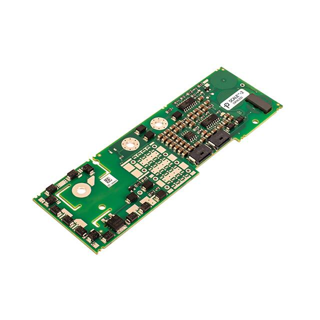
For the component position, refer to Figs. 1 and 2.
www.IGBT-Driver.com
Page 7
�1SP0635x2xx-12
Preliminary Data Sheet
Assembly Drawing
Fig. 1: Assembly drawing of 1SP0635x2Mx with highlighted gate resistors
Fig. 2: Assembly drawing of 1SP0635D2Sx with highlighted gate resistors
Note that the wires of the gate resistors should not project more than 1.6mm after soldering (excess length at
bottom side). Furthermore, a minimum distance of 1mm must be maintained between the gate resistor body
and the PCB.
Legal Disclaimer
This data sheet specifies devices but cannot promise to deliver any specific characteristics. No warranty or
guarantee is given – either expressly or implicitly – regarding delivery, performance or suitability.
CT-Concept Technologie GmbH reserves the right to make modifications to its technical data and product
specifications at any time without prior notice. The general terms and conditions of delivery of CT-Concept
Technologie GmbH apply.
www.IGBT-Driver.com
Page 8
�1SP0635x2xx-12
Preliminary Data Sheet
Ordering Information
The general terms and conditions of delivery of CT-Concept Technologie GmbH apply.
Interface
Master, Fiber-Optic Interface
Master, Fiber-Optic Interface
Slave, Electrical Interface
1)
2)
1)
2)
CONCEPT Driver Type #
Related IGBT
1SP0635V2M1-12
1SP0635S2M1-12
1SP0635D2S1-12
1200V IGBT modules
1200V IGBT modules
1200V IGBT modules
Fiber-optic interface with versatile link (HFBR-2522Z and HFBR-1522Z)
Fiber-optic interface with ST (HFBR-2412Z and HFBR-1412Z)
See “Description & Application Manual for 1SP0635 SCALE-2 IGBT Drivers”
Product home page: www.IGBT-Driver.com/go/1SP0635
Refer to www.IGBT-Driver.com/go/nomenclature for information on driver nomenclature
Information about Other Products
For other drivers, evaluation systems, product documentation and application support
Please click onto: www.IGBT-Driver.com
Manufacturer
CT-Concept Technologie GmbH
A Power Integrations Company
Johann-Renfer-Strasse 15
2504 Biel-Bienne
Switzerland
Phone
Fax
+41 - 32 - 344 47 47
+41 - 32 - 344 47 40
E-mail
Internet
Info@IGBT-Driver.com
www.IGBT-Driver.com
© 2010…2013 CT-Concept Technologie GmbH - Switzerland.
We reserve the right to make any technical modifications without prior notice.
www.IGBT-Driver.com
All rights reserved.
Version 2.1 from 2016-05-20
Page 9
�