SCALE™-2 2SP0115T2A0-12
2SP0115T2A0-12
Preliminary Data Sheet
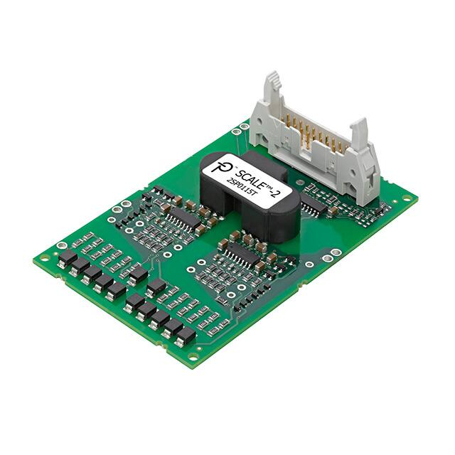
Compact, high-performance, plug-and-play dual-channel IGBT driver based on
SCALE™-2 technology for individual and parallel-connected modules
Abstract
The SCALE™-2 plug-and-play driver 2SP0115T2A0-12 is a compact dual-channel intelligent gate driver
designed for 1200V 17mm dual IGBT modules. The driver features an electrical interface with a built-in DC/DC
power supply.
The turn-on and turn-off gate resistors of both channels are not assembled in order to provide
maximum flexibility. They must be assembled by the user before start of operation. Please refer to
the paragraph on “Gate Resistor Assembly” for the recommended gate resistors.
For drivers adapted to other types of high-power and high-voltage IGBT modules, refer to
www.power.com/igbt-driver/go/plug-and-play
Features
Applications
Plug-and-play solution
Allows parallel connection of IGBT modules
Shortens application development time
Extremely reliable; long service life
Built-in DC/DC power supply
20-pin flat cable interface
Duty cycle 0... 100%
Active clamping of V at turn-off
IGBT short-circuit protection
Monitoring of supply voltage
Safe isolation to EN 50178
UL compliant
Suitable for 1200V 17mm dual IGBT modules
Gate resistors not assembled
ce
www.power.com/igbt-driver
Wind-power converters
Industrial drives
UPS
Power-factor correctors
Traction
Railroad power supplies
Welding
SMPS
Radiology and laser technology
Research
and many others
Page 1
�SCALE™-2 2SP0115T2A0-12
Preliminary Data Sheet
Safety Notice!
The data contained in this data sheet is intended exclusively for technically trained staff. Handling all highvoltage equipment involves risk to life. Strict compliance with the respective safety regulations is mandatory!
Any handling of electronic devices is subject to the general specifications for protecting electrostatic-sensitive
devices according to international standard IEC 60747-1, Chapter IX or European standard EN 100015 (i.e. the
workplace, tools, etc. must comply with these standards). Otherwise, this product may be damaged.
Important Product Documentation
This data sheet contains only product-specific data. For a detailed description, must-read application notes and
common data that apply to the whole series, please refer to “Description & Application Manual for 2SP0115T
SCALE-2 IGBT Drivers” on www.power.com/igbt-driver/go/2SP0115T.
The gate resistors on this gate driver are not assembled in order to provide maximum flexibility. For the gate
resistors required for specific IGBT modules, refer to the paragraph on “Gate Resistor Assembly”. Use of gate
resistors other than those specified may result in failure.
Mechanical Dimensions
Dimensions: Refer to “Description & Application Manual for 2SP0115T SCALE-2 IGBT Drivers”
Mounting principle: Soldered onto 17mm dual IGBT module
Absolute Maximum Ratings
Parameter
Remarks
Min
Supply voltage VCC
Logic input and output voltages
SOx current
Gate peak current Iout
Average supply current ICC
Output power per gate
Turn-on gate resistance
Turn-off gate resistance
Switching frequency f
Test voltage (50Hz/1min.)
VCC to GND
To GND
Fault condition, total current
Note 1
Note 2
Ambient temperature ≤70°C (Note 3)
Ambient temperature ≤85°C (Note 3)
Note 15
Note 15
Note 20
Primary to secondary (Note 16)
0
16
V
-0.5 VCC+0.5 V
20
mA
-8
+15
A
290
mA
1.2
W
1
W
1.3
Ω
1.8
Ω
n.d.
kHz
3800 VAC(eff)
DC-link voltage
|dV/dt|
Secondary to secondary (Note 16)
Note 4
Rate of change of input to output voltage
www.power.com/igbt-driver
Max
Unit
3800 VAC(eff)
800
V
50 kV/μs
Page 2
�SCALE™-2 2SP0115T2A0-12
Preliminary Data Sheet
Parameter
Remarks
Operating voltage
Operating temperature
Storage temperature
Primary/secondary, secondary/secondary
Note 19
Min
Max
Unit
-20
-40
1200
+85
+90
Vpeak
°C
°C
Recommended Operating Conditions
Parameter
Remarks
Min
Typ
Max
Unit
Supply voltage VCC
Resistance from TB to GND
SOx current
To GND
Blocking time≠0, ext. value
Fault condition, 3.3V logic
14.5
128
15
15.5
∞
4
V
kΩ
mA
Min
Typ
Max
Unit
Electrical Characteristics
Power Supply
Remarks
Supply current ICC
Efficiency η
Coupling capacitance Cio
Without load
Internal DC/DC converter
Primary side to secondary side, total, per channel
Power Supply Monitoring
Remarks
Min
Typ
Max
Unit
Supply threshold VCC
11.9
11.3
0.35
12.1
11.5
0.35
5
4.7
0.15
12.6
12.0
13.3
12.7
12.6
12.0
13.1
12.5
5.15
4.85
5.3
5
Monitoring hysteresis
Primary side, clear fault
Primary side, set fault (Note 5)
Primary side, set/clear fault
Secondary side, clear fault
Secondary side, set fault (Note 6)
Secondary side, set/clear fault
Secondary side, clear fault
Secondary side, set fault (Note 6)
Secondary side, set/clear fault
V
V
V
V
V
V
V
V
V
Logic Inputs and Outputs
Remarks
Min
Typ
Max
Unit
Input impedance
Turn-on threshold
Turn-off threshold
SOx output voltage
V(INx)>3V (Note 7)
V(INx) (Note 8)
V(INx) (Note 8)
Fault condition, I(SOx)550V (Note 9)
After the response time (Note 10)
After fault (Note 11)
Timing Characteristics
Remarks
Turn-on delay td(on)
Turn-off delay td(off)
Jitter of turn-on delay
Jitter of turn-off delay
Output rise time tr(out)
Output fall time tf(out)
Dead time between outputs
Jitter of dead time
Transmission delay of fault state
Note 12
Note 12
Note 18
Note 18
Gx to Ex (Note 13)
Gx to Ex (Note 13)
Half-bridge mode (Note 21)
Half-bridge mode
Note 14
Outputs
Remarks
Turn-on gate resistor Rg(on)
Turn-off gate resistor Rg(off)
Gate voltage at turn-on
Gate-voltage at turn-off
Note 15
Note 15
P=0W
P=1.2W
Gate resistance to COMx
Min
Typ
Max
10.2
5.4
1.4
90
Min
Typ
V
μs
μs
ms
Max
75
65
±2
±4
5
10
3
±50
400
Min
Typ
Unit
Unit
ns
ns
ns
ns
ns
ns
μs
ns
ns
Max
not assembled
not assembled
15
-9.2
-7.1
4.7
Unit
Ω
Ω
V
V
V
kΩ
Electrical Isolation
Remarks
Min
Typ
Max
Unit
Test voltage (50Hz/1s)
Primary to secondary side (Note 16)
3800
3850
3900
Veff
Secondary to secondary side (Note 16)
3800
3850
3900
Partial discharge extinction volt.
Primary to secondary side (Note 17)
Secondary to secondary side (Note 17)
Primary to secondary side
1220
1200
12.6
Vpeak
Vpeak
mm
Secondary to secondary side
6.6
mm
Primary to NTC
6.5
mm
Primary to secondary side
Secondary to secondary side
Primary to NTC
12.3
6.6
6.5
mm
mm
mm
Creepage distance
Clearance distance
Veff
All data refer to +25°C and VCC=15V unless otherwise specified
www.power.com/igbt-driver
Page 4
�SCALE™-2 2SP0115T2A0-12
Preliminary Data Sheet
Footnotes to the Key Data
1)
2)
3)
4)
5)
6)
7)
8)
9)
10)
11)
12)
13)
14)
15)
16)
17)
18)
19)
20)
21)
The gate current is limited by the gate resistors located on the driver.
If the specified value is exceeded, this indicates a driver overload. It should be noted that the driver is
not protected against overload.
If the specified value is exceeded, this indicates a driver overload. It should be noted that the driver is
not protected against overload. From 70°C to 85°C, the maximum permissible output power can be
linearly interpolated from the given data.
This limit is due to active clamping. Refer to the “Description & Application Manual for 2SP0115T
SCALE-2 IGBT Drivers”.
Undervoltage monitoring of the primary-side supply voltage (VCC to GND). If the voltage drops below
this limit, a fault is transmitted to the corresponding outputs and the IGBTs are switched off.
Undervoltage monitoring of the secondary-side supply voltage (Visox to Veex and Veex to COMx
which correspond with the approximate turn-on and turn-off gate-emitter voltages). If the
corresponding voltage drops below this limit, the IGBT is switched off and a fault is transmitted to the
corresponding output.
The input impedance can be modified to values
很抱歉,暂时无法提供与“2SP0115T2A0-12”相匹配的价格&库存,您可以联系我们找货
免费人工找货