2SP0320x2Ax-12
2SP0320x2Ax-12
Preliminary Data Sheet
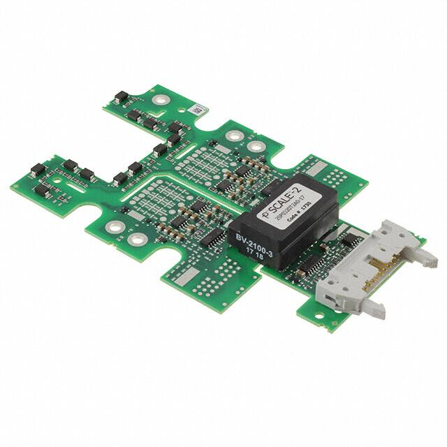
Compact, high-performance, plug-and-play dual-channel IGBT driver based on
SCALE™-2 technology for individual and parallel-connected modules in 2-level,
3-level and multilevel converter topologies
Abstract
The SCALE™-2 plug-and-play driver 2SP0320x2Ax-12 is a compact dual-channel intelligent gate driver
designed for 1200V IGBT modules from Danfoss, Fuji or Infineon. The driver features an electrical interface
(2SP0320T) or a fiber-optic interface (2SP0320V and 2SP0320S) with a built-in DC/DC power supply.
The turn-on and turn-off gate resistors of both channels are not assembled in order to provide
maximum flexibility. They must be assembled by the user before start of operation. Please refer to
the paragraph on “Gate Resistor Assembly” for the recommended gate resistors.
For drivers adapted to other types of high-power and high-voltage IGBT modules, refer to
www.IGBT-Driver.com/go/plug-and-play
Features
Applications
Plug-and-play solution
Allows parallel connection of IGBT modules
For 2-level, 3-level and multilevel topologies
Shortens application development time
Extremely reliable; long service life
Built-in DC/DC power supply
20-pin flat cable interface (2SP0320T)
Fiber-optic links (2SP0320V & 2SP0320S)
Duty cycle 0... 100%
Active clamping of V at turn-off
IGBT short-circuit protection
Monitoring of supply voltage
Safe isolation to EN 50178
UL compliant
Suitable for 1200V IGBT modules
Gate resistors not assembled
ce
www.IGBT-Driver.com
Wind-power converters
Industrial drives
UPS
Power-factor correctors
Traction
Railroad power supplies
Welding
SMPS
Radiology and laser technology
Research
and many others
Page 1
�2SP0320x2Ax-12
Preliminary Data Sheet
Safety Notice!
The data contained in this data sheet is intended exclusively for technically trained staff. Handling all highvoltage equipment involves risk to life. Strict compliance with the respective safety regulations is mandatory!
Any handling of electronic devices is subject to the general specifications for protecting electrostatic-sensitive
devices according to international standard IEC 60747-1, Chapter IX or European standard EN 100015 (i.e. the
workplace, tools, etc. must comply with these standards). Otherwise, this product may be damaged.
Important Product Documentation
This data sheet contains only product-specific data. For a detailed description, must-read application notes and
common data that apply to the whole series, please refer to “Description & Application Manual for 2SP0320T
SCALE-2 IGBT Drivers” (electrical interface) or “Description & Application Manual for 2SP0320V and 2SP0320S
SCALE-2 IGBT Drivers” (fiber-optic interface) on www.IGBT-Driver.com/go/2SP0320.
The gate resistors on this gate driver are not assembled in order to provide maximum flexibility. For the gate
resistors required for specific IGBT modules, refer to the paragraph on “Gate Resistor Assembly”. Use of gate
resistors other than those specified may result in failure.
Mechanical Dimensions
Dimensions: See the relevant “Description and Application Manual”
Mounting principle: Connected to IGBT module with screws
Fiber-Optic Interfaces
Interface
Remarks
Part type #
Drive signal input
Drive signal input
Status output
Status output
2SP0320V, fiber-optic receiver (Notes 21, 22)
2SP0320S, fiber-optic receiver (Notes 21, 22)
2SP0320V, fiber-optic transmitter (Notes 21, 23)
2SP0320S, fiber-optic transmitter (Notes 21, 23)
HFBR-2522Z
HFBR-2412Z
HFBR-1522Z
HFBR-1412Z
www.IGBT-Driver.com
Page 2
�2SP0320x2Ax-12
Preliminary Data Sheet
Absolute Maximum Ratings
Parameter
Remarks
Min
Supply voltage V DC
Supply voltage V CC
Logic input and output voltages
SO x current
Gate peak current I out
Average supply current I DC
Average supply current I DC
Output power per gate
VDC to GND
VCC to GND (Note 1)
To GND
Fault condition, total current
Note 2
2SP0320T (Note 24)
2SP0320V and 2SP0320S (Note 24)
Ambient temperature 3V (Note 6)
2SP0320T, V(INx) (Note 7)
2SP0320T, V(INx) (Note 7)
Fault condition, I(SOx) 550V (Note 8)
After the response time (Note 9)
2SP0320T, after fault (Note 10)
Efficiency η
Supply current I CC
Coupling capacitance C io
Monitoring hysteresis
Supply threshold V isox -V eex
Monitoring hysteresis
Supply threshold V eex -V COMx
www.IGBT-Driver.com
Min
Typ
Typ
10.2
6.9
1.4
90
Max
Unit
V
μs
μs
ms
Page 4
�2SP0320x2Ax-12
Preliminary Data Sheet
Timing Characteristics
Remarks
Min
Turn-on delay t d(on)
Turn-off delay t d(off)
Jitter of turn-on delay
Jitter of turn-off delay
Turn-on delay t d(on)
Turn-off delay t d(off)
2SP0320T
2SP0320T
2SP0320T
2SP0320T
2SP0320V
2SP0320V
Output rise time t r(out)
Output fall time t f(out)
G x to E x (Note 13)
G x to E x (Note 13)
Dead time between outputs
Jitter of dead time
2SP0320T, half-bridge mode
2SP0320T, half-bridge mode
Transmission delay of fault state
Transmission delay of fault state
Delay to clear fault state
(Note 11)
(Note 11)
(Note 28)
(Note 28)
and 2SP0320S (Note 12)
and 2SP0320S (Note 12)
Typ
Max
Unit
90
90
±2
±2
120
100
ns
ns
ns
ns
ns
ns
7
25
ns
ns
3
±100
μs
ns
2SP0320T (Note 14)
2SP0320V and 2SP0320S (Note 25)
2SP0320V and 2SP0320S (Note 15)
450
90
11
ns
ns
μs
Acknowledge delay time
Acknowledge pulse width
2SP0320V and 2SP0320S (Note 16)
2SP0320V and 2SP0320S (on host side)
220
700
1050
ns
ns
Outputs
Remarks
Typ
Max
Unit
Turn-on gate resistor R g(on)
Turn-off gate resistor R g(off)
Gate voltage at turn-on
Gate-voltage at turn-off
Note 17
Note 17
Min
not assembled
not assembled
15
Ω
Ω
V
-10.4/-9.9
-10.2/-9.8
-9.7/-9.5
-9.6/-9.4
4.7
V
V
V
V
kΩ
2SP0320T / (2SP0320V & 2SP0320S)
P = 0W
P = 0.3W
P = 2.1W
P = 3W
Gate resistance to COMx
dV/dt Feedback
Remarks
dV/dt feedback
Note 18
Electrical Isolation
Remarks
Min
Typ
Max
Unit
Test voltage (50Hz/1s)
Primary to secondary side (Note 19)
3800
3850
3900
V eff
Secondary to secondary side (Note 19)
3800
3850
3900
Partial discharge extinction volt.
Primary to secondary side (Note 27)
1220
V peak
Secondary to secondary side (Note 27)
1200
V peak
Primary to secondary side
20
mm
Secondary to secondary side
17
mm
Creepage distance
Implementation
No
V eff
All data refer to +25°C and V CC = V DC = 15V unless otherwise specified
www.IGBT-Driver.com
Page 5
�2SP0320x2Ax-12
Preliminary Data Sheet
Footnotes to the Key Data
1)
2)
3)
4)
5)
6)
7)
8)
9)
10)
11)
12)
13)
14)
15)
16)
17)
18)
19)
20)
21)
22)
23)
24)
Both supply voltages V DC and V CC should be applied in parallel.
The gate current is limited by the gate resistors located on the driver.
If the specified value is exceeded, this indicates a driver overload. It should be noted that the driver is
not protected against overload. From 70°C to 85°C, the maximum permissible output power can be
linearly interpolated from the given data.
This limit is due to active clamping. Refer to “Description & Application Manual for 2SP0320T SCALE-2
IGBT Drivers” (electrical interface) or “Description & Application Manual for 2SP0320V and 2SP0320S
SCALE-2 IGBT Drivers” (fiber-optic interface).
Undervoltage monitoring of the primary-side supply voltage (VCC to GND). If the voltage drops below
this limit, a fault is transmitted to the corresponding output(s) (2SP0320T/2SP0320V/2SP0320S) and
the IGBTs are switched off (only 2SP0320T).
The input impedance can be modified to values < 18 kΩ (customer-specific solution).
Turn-on and turn-off threshold values can be increased (customer-specific solution).
The resulting pulse width of the direct output of the gate drive unit for short-circuit type I (excluding
the delay of the gate resistors) is the sum of response time plus delay to IGBT turn-off.
The turn-off event of the IGBT is delayed by the specified time after the response time.
Factory set value. The blocking time can be reduced with an external resistor. Refer to “Description &
Application Manual for 2SP0320T SCALE-2 IGBT Drivers”.
Measured from the transition of the turn-on or turn-off command at the driver input to direct output
of the gate drive unit (excluding the delay of the gate resistors).
Including the delay of the external fiber-optic links. Measured from the transition of the turn-on or
turn-off command at the optical transmitter on the host controller side to the direct output of the gate
drive unit (excluding the delay of the gate resistors).
Refers to the direct output of the gate drive unit (excluding the delay of the gate resistors).
Transmission delay of the fault state from the secondary side to the primary status outputs.
Measured on the host side. The fault status on the secondary side is automatically reset after the
specified time.
Including the delay of the external fiber-optic links. Measured from the transition of the turn-on or
turn-off command at the optical transmitter on the host controller side to the transition of the
acknowledge signal at the optical receiver on the host controller side.
The gate resistors are not assembled on this IGBT gate driver. They must be assembled by the user
according to the paragraph on “Gate Resistor Assembly”.
A dV/dt feedback can optionally be implemented in order to reduce the rate of rise of the collector
emitter voltage of the IGBTs at turn-off (customer-specific solution).
HiPot testing (= dielectric testing) must generally be restricted to suitable components. This gate
driver is suited for HiPot testing. Nevertheless, it is strongly recommended to limit the testing time to
1s slots as stipulated by EN 50178. Excessive HiPot testing at voltages much higher than 850V AC(eff)
may lead to insulation degradation. No degradation has been observed over 1min. testing at
3800V AC(eff) . Every production sample shipped to customers has undergone 100% testing at the given
value or higher (
很抱歉,暂时无法提供与“2SP0320T2A0-12”相匹配的价格&库存,您可以联系我们找货
免费人工找货- 国内价格 香港价格
- 1+1614.554371+208.40708
- 10+1564.8460210+201.99071
- 40+1448.1666240+186.92970