CHY100
ChiPhy™ Family
Charger Interface Physical Layer IC
Product Highlights
VOUT
• Fully supports Quick Charge 2.0 specification
D+
• Class A: 5 V, 9 V, and 12 V output voltage
D-
• Class B: 5 V, 9 V, 12 V, and 20 V output voltage
GND
• USB battery charging specification revision 1.2 compatible
• Automatic USB DCP shorting D+ to D- line
• Default 5 V mode operation
• Supports TOPSwitch and TinySwitch
BP
• Very low power consumption
V3
• Below 1 mW at 5 V output
• Fail safe operation
• Adjacent pin-to-pin short-circuit fault
V2
Feedback
Network
D+
CHY100
U1
V1
DR
• Open circuit pin fault
GND
Typical Applications
• Battery chargers for smart phones, tablets, netbooks, digital
cameras, and bluetooth accessories
• USB power output ports
PI-6988-071713
Figure 1. Typical Application Schematic.
Description
CHY100 is a low-cost USB high-voltage dedicated charging port
(HVDCP) interface IC for the Quick Charge 2.0 specification. It
incorporates all necessary functions to add Quick Charge 2.0 capability
to Power Integrations’ switcher ICs such as TOPSwitch or TinySwitch and
other solutions employing traditional feedback schemes.
CHY100 supports the full output voltage range of either Class A or
Class B. Optionally Class B can be inhibited for protecting the battery
charger from accidental damage.
CHY100 automatically detects whether a connected Powered Device
(PD) is Quick Charge 2.0 capable before enabling output voltage
adjustment. If a PD not compliant to Quick Charge 2.0 is detected the
CHY100 disables output voltage adjustment to ensure safe operation
with legacy 5 V only USB PDs.
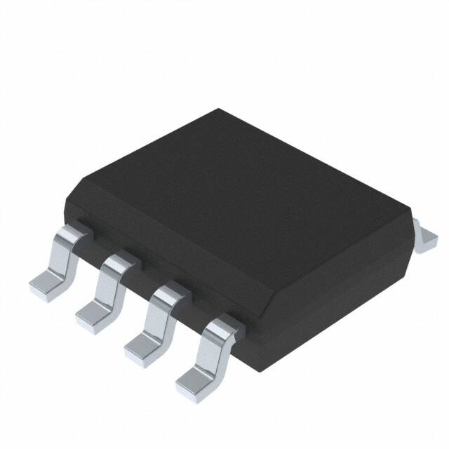
SO-8 (D Package)
Figure 2. Package Option.
www.power.com
August 2016
This Product is Covered by Patents and/or Pending Patent Applications.
�CHY100
BYPASS
(BP)
REFERENCE
(R)
BANDGAP
+
3.9 V
6V
+
2V
GND
+
0.325 V
OUTPUT
INHIBIT
V3
N3
V2
D+
CONTROL
LOGIC
S
(LOOKUP
TABLE)
R
SET
Q
N5
CLR
D-
Q
+
V1
0.325 V
N2
19.58 kΩ
+
2V
N1
GROUND
(GND)
N4
PI-7009-071513
Figure 3. Functional Block Diagram.
Pin Functional Description
GROUND (GND) Pin
Ground.
V1 Pin
Open Drain input of output voltage adjustment switch.
Active for 9 V, 12 V, and 20 V output setting.
V2 Pin
Open Drain input of output voltage adjustment switch.
Active for 12 V, and 20 V output setting.
V3 Pin
Open Drain input of output voltage adjustment switch.
Active for 20 V output setting.
D Package (SO-8)
GND
V1
V2
V3
1
8
2
7
3
6
4
5
BYPASS (BP) Pin
Connection point for an external bypass capacitor for the internally
generated supply voltage.
REFERENCE (R) Pin
Connected to internal band-gap reference. Provides reference
current through connected resistor.
BP
R
D+
D-
PI-6987-071213
Figure 4. Pin Configuration.
DATA LINE D+ Pin
USB D+ data line input.
DATA LINE D- Pin
USB D- data line input.
2
Rev. E 08/18
www.power.com
�CHY100
Functional Description
CHY100 is a low-cost USB high-voltage dedicated charging port
(HVDCP) interface IC for the Quick Charge 2.0 specification. It
incorporates all necessary functions to add Quick Charge 2.0
capability to Power Integrations’ integrated switcher ICs such as
TOPSwitch or TinySwitch.
CHY100 also supports other solutions with traditional feedback
schemes like optocoupler and secondary reference regulator TL431 as
depicted in Figure 5.
VOUT
D1
C1
R6
D+
R1
D-
RDAT_LKG
RBP
GND
CBP
U3
BP
C6
R5 V3
R4 V2
U1
TL431
R3 V1
R2
D+
CHY100
U2
DR
GND
RREF
PI-7008-071613
Figure 5. CHY100 with Traditional Output Regulation (CV Only).
CHY100 supports the full output voltage range of Quick Charge 2.0
Class A (5 V, 9 V, or 12 V) or Class B (5 V, 9 V, 12 V, or 20 V). It
automatically detects either Quick Charge 2.0 capable powered devices
(PD) or legacy PDs compliant with the USB Battery Charging
Specification revision 1.2 and only enables output voltage adjustment
accordingly.
Shunt Regulator
The internal shunt regulator clamps the BYPASS pin at 6 V when
current is provided through an external resistor (RBP in Figure 5). This
facilitates powering of CHY100 externally over the wide power supply
output voltage range of 5 V to 20 V. Recommended values are RBP =
4.53 kΩ and CBP = 220 nF.
Quick Charge 2.0 Interface
At power-up CHY100 turns on switch N5 (see Figure 3) in 20 ms or
less after the BYPASS pin voltage has reached 4 V. Switch N4 and
output switches N1 to N3 remain off. This sets the default 5 V output
voltage level. With D+ and D- short-circuited the normal handshake
between the AC-DC adapter (DCP) and powered devices (PD) as
described in the USB Battery Charging Specification 1.2 can commence. After switch N5 has been turned on CHY100 starts monitoring the voltage level at D+. If it continuously stays above VDAT(REF)
(typ. 0.325 V) and below VSEL(REF) (typ. 2 V) for at least 1.25 seconds
CHY100 will enter Quick Charge 2.0 operation mode. If the voltage at
D+ drops any time below 0.325 V CHY100 resets the 1.25 seconds
timer and stays in USB Battery Charging Specification 1.2 compatibility
mode with a default output voltage of 5 V.
Once CHY100 has entered Quick Charge 2.0 operation mode switch
N5 will be turned off. Additionally switch N4 is turned on connecting
a 19.53 kΩ pull-down resistor to D-. As soon as the voltage at D- has
dropped low ( ±2000 V on all pins
Machine Model ESD
JESD22-A115C
> ±200 V on all pins
> ±100 mA or > 1.5 V (max) on all pins
Part Ordering Information
• ChiPhy Product Family
• 100 Series Number
• Package Identifier
CHY 100
D
D
SO-8
7
www.power.com
Rev. E 08/16
�Revision Notes
Date
A
Initial Release.
07/13
B
Extended Ambient Temperature to -40 °C.
01/14
C
Added Note for Class A Charger on page 3.
03/14
D
Updated with new Brand Style.
06/15
E
Added Package Marking, MSL Table, ESD and Latch-Up Table.
08/16
For the latest updates, visit our website: www.power.com
Power Integrations reserves the right to make changes to its products at any time to improve reliability or manufacturability. Power Integrations
does not assume any liability arising from the use of any device or circuit described herein. POWER INTEGRATIONS MAKES NO WARRANTY
HEREIN AND SPECIFICALLY DISCLAIMS ALL WARRANTIES INCLUDING, WITHOUT LIMITATION, THE IMPLIED WARRANTIES OF MERCHANTABILITY,
FITNESS FOR A PARTICULAR PURPOSE, AND NON-INFRINGEMENT OF THIRD PARTY RIGHTS.
Patent Information
The products and applications illustrated herein (including transformer construction and circuits external to the products) may be covered by one
or more U.S. and foreign patents, or potentially by pending U.S. and foreign patent applications assigned to Power Integrations. A complete list of
Power Integrations patents may be found at www.power.com. Power Integrations grants its customers a license under certain patent rights as set
forth at http://www.power.com/ip.htm.
Life Support Policy
POWER INTEGRATIONS PRODUCTS ARE NOT AUTHORIZED FOR USE AS CRITICAL COMPONENTS IN LIFE SUPPORT DEVICES OR SYSTEMS
WITHOUT THE EXPRESS WRITTEN APPROVAL OF THE PRESIDENT OF POWER INTEGRATIONS. As used herein:
1. A Life support device or system is one which, (i) is intended for surgical implant into the body, or (ii) supports or sustains life, and (iii) whose
failure to perform, when properly used in accordance with instructions for use, can be reasonably expected to result in significant injury or
death to the user.
2. A critical component is any component of a life support device or system whose failure to perform can be reasonably expected to cause the
failure of the life support device or system, or to affect its safety or effectiveness.
The PI logo, TOPSwitch, TinySwitch, SENZero, SCALE-iDriver, Qspeed, PeakSwitch, LYTSwitch, LinkZero, LinkSwitch, InnoSwitch, HiperTFS,
HiperPFS, HiperLCS, DPA-Switch, CAPZero, Clampless, EcoSmart, E-Shield, Filterfuse, FluxLink, StakFET, PI Expert and PI FACTS are trademarks of
Power Integrations, Inc. Other trademarks are property of their respective companies. ©2016, Power Integrations, Inc.
Power Integrations Worldwide Sales Support Locations
World Headquarters
5245 Hellyer Avenue
San Jose, CA 95138, USA.
Main: +1-408-414-9200
Customer Service:
Phone: +1-408-414-9665
Fax: +1-408-414-9765
e-mail: usasales@power.com
China (Shanghai)
Rm 2410, Charity Plaza, No. 88
North Caoxi Road
Shanghai, PRC 200030
Phone: +86-21-6354-6323
Fax: +86-21-6354-6325
e-mail: chinasales@power.com
Germany
Lindwurmstrasse 114
80337 Munich
Germany
Phone: +49-895-527-39110
Fax: +49-895-527-39200
e-mail: eurosales@power.com
Germany
HellwegForum 1
59469 Ense
Germany
Tel: +49-2938-64-39990
e-mail: igbt-driver.sales@
power.com
India
China (Shenzhen)
#1, 14th Main Road
17/F, Hivac Building, No. 2, Keji Nan Vasanthanagar
8th Road, Nanshan District,
Bangalore-560052 India
Shenzhen, China, 518057
Phone: +91-80-4113-8020
Phone: +86-755-8672-8689
Fax: +91-80-4113-8023
Fax: +86-755-8672-8690
e-mail: indiasales@power.com
e-mail: chinasales@power.com
Italy
Via Milanese 20, 3rd. Fl.
20099 Sesto San Giovanni (MI) Italy
Phone: +39-024-550-8701
Fax: +39-028-928-6009
e-mail: eurosales@power.com
Japan
Kosei Dai-3 Bldg.
2-12-11, Shin-Yokohama,
Kohoku-ku
Yokohama-shi, Kanagawa
222-0033 Japan
Phone: +81-45-471-1021
Fax: +81-45-471-3717
e-mail: japansales@power.com
Korea
RM 602, 6FL
Korea City Air Terminal B/D, 159-6
Samsung-Dong, Kangnam-Gu,
Seoul, 135-728, Korea
Phone: +82-2-2016-6610
Fax: +82-2-2016-6630
e-mail: koreasales@power.com
Singapore
51 Newton Road
#19-01/05 Goldhill Plaza
Singapore, 308900
Phone: +65-6358-2160
Fax: +65-6358-2015
e-mail: singaporesales@power.com
Taiwan
5F, No. 318, Nei Hu Rd., Sec. 1
Nei Hu Dist.
Taipei 11493, Taiwan R.O.C.
Phone: +886-2-2659-4570
Fax: +886-2-2659-4550
e-mail: taiwansales@power.com
UK
Cambridge Semiconductor,
a Power Integrations company
Westbrook Centre, Block 5, 2nd Floor
Milton Road
Cambridge CB4 1YG
Phone: +44 (0) 1223-446483
e-mail: eurosales@power.com
�