LNK454/456-458/460 LinkSwitch-PL Family
®
LED Driver IC with TRIAC Dimming, Single-Stage PFC and Constant Current Control for Non-Isolated Applications
Product Highlights
Dramatically Simplifies Off-line LED Drivers • Single stage power factor correction and accurate constant current (CC) output • Flicker-free phase-controlled TRIAC dimming • Very low component count with small non-electrolytic bulk capacitor, for compact replacement lamp designs • Compact SO8 package • Completely eliminates control loop compensation Advanced Performance Features • Optimized for non-isolated flyback designs • Frequency jitter greatly reduces EMI filter size and costs • Low dissipation direct sensing of LED current
PR EL IM IN AR Y
D CONTROL S FB
AC IN
LinkSwitch-PL
BP
PI-5835-060710
Advanced Protection and Safety Features • 725 V integrated MOSFET allows small bulk capacitance and maximizes power capability • Latching shutdown protection for short-circuit / open feedback and output overvoltage • Auto-restart for overload condition • Hysteretic thermal shutdown • Meets high-voltage creepage between DRAIN and all other pins both on PCB and at package EcoSmart ® - Energy Efficient • High power factor optimizes system lumen per watt by reducing input VA • Control algorithm balances switching and conduction losses over line and load to maintain optimum efficiency • Cycle skipping regulation for abnormally low output power to clamp peak output current delivered
Figure 1.
Basic Application Schematic.
Output Power Table
Product 2
LNK454D LNK456D LNK457D/V LNK458V LNK460V
85-265 VAC Minimum Output Maximum Output Power1 Power1 1.5 W 3W 3W 6W 4W 8W 6W 11.5 W 8W 16 W
Table 1. Output Power Table. Notes: 1. Maximum practical continuous power in an open frame design with adequate heat sinking, measured at +50 °C ambient (see Key Applications Considerations for more information). 2. Packages: D: SO-8C, V: eDIP-12.
Description
Output Current
700 mA LNK454 LNK456 LNK457 LNK458 LNK460 LNK460 1000 mA LNK456 LNK457 LNK458 LNK460
The LinkSwitch-PL family enables a very small and low cost single-stage power factor corrected constant current driver for solid state lighting. Optimized for direct LED current sensing, the LinkSwitch-PL operates over a wide input voltage range delivering an output power of up to 16 W. The LinkSwitch-PL control algorithm provides flicker-free TRIAC dimming with minimal external components.
Each device incorporates a 725 V rated power MOSFET, a novel discontinuous mode variable frequency variable on-time controller, frequency jitter, cycle by cycle current limit and hysteretic thermal shutdown in a monolithic 4-pin IC, available in SO-8C and eDIP-12 packages.
Number of Serial LEDs 1 2 3 4 5 6 7 8 9 10 11 12
350 mA
500 mA
LNK454 LNK454 LNK456 LNK456 LNK457 LNK457 LNK458 LNK458 LNK458 LNK460 LNK460 LNK460
LNK454 LNK456 LNK456 LNK457 LNK458 LNK458 LNK460 LNK460 LNK460
Figure 2.
Device Selection based on Length of Output LED Series String and Current. A Typical Voltage Drop of 3.5 V per LED is Assumed.
www.powerint.com
This document contains information on a new product. Specifications and information herein are subject to change without notice.
PRELIMINARY
June 2010
�LNK454/456-458/460
BYPASS (BP) UV 4.9 V ILIM
REGULATOR 5.85 V
DRAIN (D)
ILIM
+
V_ILIM SOA Q VFB(SK)
+
SET
S
CURRENT LIMIT SOA STATE MACHINE
Q
CLR
R
UV
VFB(LO)
+
IFB 1 µA
VREF DAC
PHASE MEASUREMENT
Zero Crossing
+
V_ZLIM
PR EL IM IN AR Y
FEEDBACK (FB)
+
FILTER
DIGITAL INTEGRATOR
AUTO-RESTART
Update CLK
INC/DEC
VARIABLE FREQUENCY/ DUTY CONTROLLER
S
SET
Q
R
CLR
Q
ON-TIME EXTENSION
PI-5893-060210
SOURCE (S)
Figure 2.
Functional Block Diagram.
Pin Functional Description
DRAIN (D) Pin: High-voltage power MOSFET drain connection. The internal start-up bias current is drawn from this pin through a switched high-voltage current source. Drain current sensing and associated controller functions are also performed using this pin. SOURCE (S) Pin: Power MOSFET source connection. Ground reference for BYPASS and FEEDBACK pins. BYPASS (BP) Pin: Connection point for the external bypass capacitor for the internally generated 5.85 V supply.
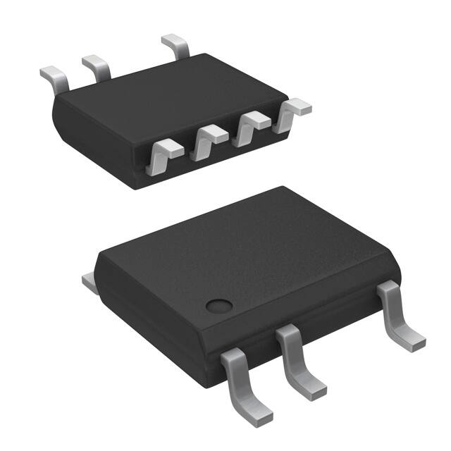
D Package (SO-8C)
8 7 6 5 S S S S
FB
1 2
BP
D
4
Exposed Pad Internally Connected to SOURCE Pin
V Package (eDIP-12)
1 NC 2 FB 3 BP 4 NC 5 NC 6D
PI-5836a-0526–10
FEEDBACK (FB) Pin: LED current sensing pin. During normal operation the 290 mV threshold determines the average value of the current flowing through the load sense resistor.
S 12 S 11
S 10 S9 S8
A second higher threshold clamps excessive output current ripple. An additional higher threshold is used to protect against output short-circuit and overvoltage conditions.
S7
Figure 3.
Pin Configuration (Top View).
2
Rev. A 06/10
This document contains information on a new product. Specifications and information herein are subject to change without notice.
PRELIMINARY
www.powerint.com
�LNK454/456-458/460
DES
DZOV
AC IN
RES
D
ROV
LinkSwitch-PL
CONTROL BP
Figure 4.
Functional Description
The LinkSwitch-PL combines a high-voltage power MOSFET switch with a power supply controller in one device. The IC provides a single stage power factor correction plus LED current control. The LinkSwitch-PL controller consists of an oscillator, feedback (sense and logic) circuit, 5.85 V regulator, hysteretic over-temperature protection, frequency jittering, cycle-by-cycle current limit, loop compensation circuitry, autorestart, switching on-time extension, power factor and constant current control. In a direct LED current sensing configuration, the average FEEDBACK pin voltage is a replica of the LED current, scaled by the sense resistor (RSENSE in Figure 4). A small low-pass filter (RF and CF in Figure 4) reduces high frequency noise at the FEEDBACK pin. Figure 5 illustrates the operating regions of the FEEDBACK pin voltage. The LinkSwitch-PL sets its operating point such that the average FEEDBACK pin voltage in steady-state operation is 290 mV. This threshold is low to minimize the sensing resistor dissipation. The internal MOSFET switching frequency and on-time are updated once every input AC half-cycle to regulate the output current and maintain high power factor.
PR EL IM IN AR Y
CF RSENSE RF
Typical Application Schematic.
S
FB
PI-5837-060710
Latching shutdown protection is triggered by a FEEDBACK pin voltage in excess of 2 V. This feature can be used to provide output overvoltage protection (via DZOV and ROV, in Figure 4), which triggers the IC to latch off. This condition is reset when the BYPASS pin voltage drops below 4.9 V, after removal of the AC input.
Latch Off
2V
Cycle Skipping Mode
If the FEEDBACK pin peak voltage exceeds 520 mV, cycle skipping mode is triggered and the power processed by the integrated MOSFET is clamped on a cycle-by-cycle basis. Switching frequency may vary during an input voltage half-cycle to reduce thermal stress on the output LEDs.
520 mV
Normal Operation
290 mV
PI-5838-041910
Figure 5.
FEEDBACK Pin Operation Voltage Thresholds.
www.powerint.com
This document contains information on a new product. Specifications and information herein are subject to change without notice.
PRELIMINARY
3
Rev. A 06/10
�LNK454/456-458/460
VFB ϕOS ϕOL ϕOL ϕOS
VFB(ϕ)
VFB(ϕ)
Phase Angle
Phase Angle 0° 180°
PR EL IM IN AR Y
0° 180° VLINE VTRIAC ϕ Phase Angle ϕ 0° Phase Angle TRIAC Conduction 0° TRIAC Conduction Phase Angle Leading Edge TRIAC Dimmers Trailing Edge TRIAC Dimmers
Feedback Voltage vs. Phase Angle Dimming Characteristics.
Phase Angle
PI-5894a-052610
Figure 6.
TRIAC (Phase-Controlled) Dimming
The LinkSwitch-PL integrates several features to improve dimming range and reduce external circuit complexity when using a phase-controlled TRIAC dimmer. The output LED current is controlled by the FEEDBACK pin voltage which changes proportionally to the TRIAC dimmer conduction angle. The conduction angle decreases, the voltage at the FEEDBACK pin decreases causing the average LED current to decrease. The FEEDBACK pin voltage adjustment is initiated at approximately 20% of the main half-cycle duration. When this (jOS) threshold is exceeded, VFB and the output LED current are reduced until a second phase angle threshold is reached. When this happens, with the TRIAC conduction angle being
very limited, the IC runs open loop (j OL region) and the integrated MOSFET processes as much power as the heavily chopped input voltage will allow creating a light output that is deeply dimmed. The 520 mV clamping feedback threshold is also linearly reduced during dimming to control LED current ripple. To help maintain the holding current of the TRIAC in the dimmer, LinkSwitch-PL extends the MOSFET on-time towards the zero crossings of the AC input voltage providing an active bleed or holding current function. This on-time extension is carefully limited to avoid deterioration of input current harmonic content and limit total harmonic distortion (THD).
4
Rev. A 06/10
This document contains information on a new product. Specifications and information herein are subject to change without notice.
PRELIMINARY
www.powerint.com
�LNK454/456-458/460
IC Supply and BYPASS Pin The internal 5.85 V regulator charges the bypass capacitor connected to the BYPASS pin to 5.85 V by drawing current from the voltage on the DRAIN pin whenever the power MOSFET is off. The BYPASS pin is the internal supply voltage node. When the power MOSFET is on, the device operates from the energy stored in the bypass capacitor. Extremely low power consumption of the internal circuitry allows LinkSwitch-PL to operate continuously from current it takes from the DRAIN pin. A bypass capacitor value of 1 µF is sufficient for both high frequency decoupling and energy storage. During phase angle dimming when the conduction angle is small the AC input voltage is present for only short periods of time. In that case the IC should not rely on the integrated high voltage current source, but instead external bias circuitry should be used to supply the IC from the output (DES and RES in Figure 4). If the output voltage is less than 7 V, external bias circuitry should be implemented, by using a bias winding on the primary of the transformer with a small signal rectifier and an electrolytic capacitor with a value based on maximum IC consumption and maximum phase dimming conduction angles. Start-up, Switching Frequency, On-time Range At start-up the controller uses an initial switching frequency fMIN and minimum on-time tON(MIN). The charging of the output capacitor together with the energy delivery to the output LEDs as soon as their anode-cathode threshold is reached determines a step-by-step increase of the operating power MOSFET switching frequency and on-time every half-cycle of the main input voltage. properly designed supply will not operate in this mode under normal load conditions. A power supply designed correctly will operate within the switching frequency range [fMIN … fMAX ], with an on-time falling between tON(MIN) and tON(MAX) when connected to a normal load. Overload Protection In case of overload, the system will increase the operating frequency and on-time each AC half-cycle until the maximum frequency and maximum on-time are reached. When this state is reached, by the next half-cycle, the controller will enter auto-restart protection, thus inhibiting the gate of the power MOSFET for approximately 1.28 s if the main line frequency is 50 Hz, 1.02 s if it is 60 Hz. After this auto-restart off-time expires, the circuit will start again, exactly as at start-up, i.e. at fMIN and tON(MIN), stepping up until regulation is achieved again. In case of a persistent overload condition, the auto-restart duty cycle DCAR will typically be as low as 33%. Auto-restart is inhibited during phase dimming when the TRIAC conduction duty cycle is less than 60%. Output Overvoltage Protection If a no-load condition is present on the output of the supply, the output overvoltage Zener (DZOV in Figure 4) will conduct once its threshold is reached. A voltage VOV in excess of VFB(LO) = 2 V will appear across the FEEDBACK pin and the IC will latch off. Normal operation will be restored once the BYPASS pin voltage drops below 4.9 V and the IC goes through a new start-up phase. Output Short-Circuit If the output of the supply (i.e. the LED load) is short-circuited, then a large amount of energy will be delivered to the sense resistor, generating a high voltage at the FEEDBACK pin. If this condition develops more than 2 V on the FEEDBACK pin, then the IC will interpret this event as an output short-circuit and will trigger latching shutdown. Normal operation will resume after cycling the AC input such that the BYPASS pin voltage drops below 4.9 V and the IC goes through a new start-up phase. Safe Operating Area (SOA) Protection If 3 consecutive cycles of the power MOSFET are prematurely terminated due to the power MOSFET current exceeding the current limit after the leading edge blanking time, SOA protection mode is triggered and the IC will trigger latching shutdown. Normal operation will resume after cycling the AC input such that the BYPASS pin voltage drops below 4.9 V and the IC goes through a new start-up phase. Hysteretic Thermal Shutdown The thermal shutdown circuitry senses the die junction temperature. The thermal shutdown threshold is set to 142 °C typical with a 75 °C hysteresis. When the die temperature rises above this threshold (142 °C) the power MOSFET is disabled and remains disabled until the die temperature falls by 75 °C, at which point the power MOSFET is re-enabled.
When the operating conditions (start-up or large transients) allow for only low energy processing (low frequency and on-time), the voltage across the input bulk capacitance will not reach zero even if the main voltage crosses zero. During these conditions the IC sets the reference voltage on the FEEDBACK pin to one half of its preset level (145 mV), to avoid overshoot of the output LED current. Once the FEEDBACK pin voltage exceeds this reduced threshold (with the zero crossing on the bulk capacitor being achieved), then the FEEDBACK pin voltage is restored to the normal 290 mV level. The steady state switching frequency and on-time is determined by the line voltage, voltage drop across the LEDs and system overall power transfer efficiency. At light load when the device reaches the minimum frequency fMIN and on-time tON(MIN), the controller regulates by skipping cycles. In this mode of operation the input current is not power factor corrected and the average output current is not guaranteed to fall within the normal range. The FEEDBACK pin cycle skipping threshold is reduced from approximately twice the normal regulation level down to just above the level required to limit output power delivery under these conditions. A
PR EL IM IN AR Y
PRELIMINARY
www.powerint.com
This document contains information on a new product. Specifications and information herein are subject to change without notice.
5
Rev. A 06/10
�LNK454/456-458/460
Absolute Maximum Ratings(1,4) DRAIN Pin Peak Current: LNK454 ................. 400 mA (750 mA) LNK456 ................850 mA (1450 mA) LNK457 ............. 1350 mA (2000 mA) LNK458 .............. 1750 mA (2650 mA) LNK460 .............. 2700 mA (5100 mA) DRAIN Pin Voltage ……………………… ............. -0.3 V to 725 V FEEDBACK Pin Voltage ……………………… ............ -0.3 to 9 V BYPASS Pin Voltage ……………………… ................. -0.3 to 9 V Lead Temperature(3) ....................................................... .........260 °C Storage Temperature …………………. .................. -65 to 150 °C Operating Junction Temperature(2).........................-40 to 150 °C Notes: 1. All voltages referenced to SOURCE, TA = 25 °C. 2. Normally limited by internal circuitry. 3. 1/16 in. from case for 5 seconds. 4. The Absolute Maximum Ratings specified may be applied, one at a time without causing permanent damage to the product. Exposure to Absolute Maximum Ratings for extended periods of time may affect product reliability.
Thermal Resistance: D (SO-8C) Package: (qJA) .................................. 100 °C/W(1), 80 °C/W(2) (qJC) ............................................... ........ 30 °C/W(3) V (eDIP) Package: (qJA) .................................... 68 °C/W(1), 58 °C/W(2) (qJC) ............................................... ...........2 °C/W(4)
PR EL IM IN AR Y
Parameter Symbol Conditions SOURCE = 0 V; TJ = -40 to +125 °C (Unless Otherwise Specified) Min Typ
fMAX TJ = 25 °C Average 110 122 6 Peak-Peak Jitter Average fMIN TJ = 25 °C 25.8 28.7 6 Peak-Peak Jitter tON(MAX) tON(MIN) tEXT TJ = 25 °C TJ = 25 °C 5.74 1.18 5.2 70 DCMAX VFB TJ = 25 °C 275 290 520 VFB(SK) VFB(LO) IFB -1.3 2000 -1.0 6
Thermal Resistance
Notes: 1. Soldered to 0.36 sq. in. (232 mm2), 2 oz. (610g/m2) copper clad, with no external heat sink attached. 2. Soldered to 1 sq. in. (645 mm2), 2 oz. (610g/m2) copper clad, with no external heat sink attached. 3. Measured on the SOURCE pin close to plastic interface. 4. Measured at the surface of exposed pad.
Max
Units
Control Functions Maximum Output Frequency Minimum Output Frequency
134
kHz %
31.6
kHz % µs µs µs %
Maximum Switch ON-Time Minimum Switch ON-Time
ON-Time Extension
Maximum Duty Cycle
FEEDBACK Pin Voltage FEEDBACK Pin Voltage Triggering Cycle Skipping Mode FEEDBACK Pin Voltage for IC Latch-OFF Feedback Pull-up Current
305
mV mV
mV -0.7 µA
Rev. A 06/10
This document contains information on a new product. Specifications and information herein are subject to change without notice.
PRELIMINARY
www.powerint.com
�LNK454/456-458/460
Parameter
Control Function (cont.)
Symbol
Conditions SOURCE = 0 V; TJ = -40 to +125 °C (Unless Otherwise Specified)
Min
Typ
Max
Units
IS1
VFB > VFB(SK) (MOSFET not switching) LNK454
450 530 585 650 730 1050 -4.2 -5.9 -8.5 -2.4 -3.7 -5.7
µA
DRAIN Supply Current IS2
VFB = 0 V (MOSFET switching at fMAX)
LNK456 LNK457 LNK458 LNK460 LNK454 LNK460 LNK454 LNK460
µA
PR EL IM IN AR Y
ICH1 VBP = 0 V, TJ = 25 °C -5.9 -8.3 -3.4 -5.2 -8.0 LNK456/457/458 -11.9 ICH2 VBP VBP = 4 V, TJ = 25 °C LNK456/457/458 5.60 5.85 di/dt = 160 mA/µs TJ = 25 °C di/dt = 325 mA/µs TJ = 25 °C di/dt = 490 mA/µs TJ = 25 °C di/dt = 650 mA/µs TJ = 25 °C di/dt = 980 mA/µs TJ = 25 °C LNK454 LNK456 LNK457 LNK458 LNK460 245 491 790 264 528 850 ILIMIT(MIN) 1023 1581 160 1100 1700 200 150 142 75 tLEB tILD TJ = 25 °C TJ = 25 °C TSD 135 TSD(H) VBP(RESET) 4.9 This document contains information on a new product. Specifications and information herein are subject to change without notice.
-2.5 -3.5 -5.1 -1.4 -2.2 -3.4 6.15 V mA mA
BYPASS Pin Charge Current
BYPASS Pin Voltage Circuit Protection
283 565 910 1177 1819 ns ns 150 °C °C V mA
Current Limit
Leading Edge Blanking Time
Current Limit Delay Thermal Shutdown Temperature Thermal Shutdown Hysteresis
BYPASS Pin Power-up Reset Threshold Voltage
PRELIMINARY
7
Rev. A 06/10
www.powerint.com
�LNK454/456-458/460
Parameter
Output
Symbol
Conditions SOURCE = 0 V; TJ = -40 to +125 °C (Unless Otherwise Specified)
Min
Typ
Max
Units
LNK454 ID = 26 mA LNK456 ID = 53 mA ON-State Resistance RDS(ON) LNK457 ID = 85 mA LNK458 ID = 110 mA LNK460 ID = 170 mA
TJ = 25 °C TJ = 100 °C TJ = 25 °C TJ = 100 °C TJ = 25 °C TJ = 100 °C TJ = 25 °C
23.1 34.4 11.7 17.5 6.9 10.4 4.4 6.7
26.6 39.8 13.5 20.2 7.9 11.9 5.1 7.6 2.6 3.9 50 µA V V s % W
OFF-State Leakage
Breakdown Voltage
DRAIN Supply Voltage
Auto-Restart OFF-Time
Auto-Restart Duty Cycle
PR EL IM IN AR Y
TJ = 100 °C TJ = 25 °C 2.2 3.3 TJ = 100 °C IDSS1 VBP = 6.2 V, VFB > VFB(SK) , VDS = 580 V, TJ = 125 °C VBP = 6.2 V, VFB > VFB(SK), TJ = 25 °C BVDSS 725 50 tAR(OFF) DCAR fMAIN = 50 Hz fMAIN = 60 Hz 1.28 1.02 33 8 This document contains information on a new product. Specifications and information herein are subject to change without notice.
PRELIMINARY
Rev. A 06/10
www.powerint.com
�LNK454/456-458/460
Typical Performance Characteristics
PI-6005-060210
DRAIN Capacitance (pF)
Power (mW)
100
Scaling Factors: LNK454 0.3 LNK456 0.6 LNK457 1.0 LNK458 1.55 LNK460 3.1
100 90 80 70 60 50 40 30 20 10
Scaling Factors: LNK454 0.3 LNK456 0.6 LNK457 1.0 LNK458 1.55 LNK460 3.1
10
PR EL IM IN AR Y
0 100 200 300 400 500 600 0
0
0
100 200 300 400 500 600 700
DRAIN Voltage (V)
DRAIN Voltage (V)
Figure 7.
Drain Capacitance vs. Drain Voltage.
Figure 8.
Power vs. Drain Voltage.
1
DRAIN Current (A)
0.8
0.6 0.4 0.2
Scaling Factors: LNK454 0.3 LNK456 0.6 LNK457 1.0 LNK458 1.55 LNK460 3.1
LNK457 TCASE = 25 °C LNK457 TCASE = 100 °C
0
0
2
4
6
8 10 12 14 16 18 20
DRAIN Voltage (V)
Figure 9.
Drain Current vs. Drain Voltage.
www.powerint.com
This document contains information on a new product. Specifications and information herein are subject to change without notice.
PRELIMINARY
PI-6006-060210
1.2
PI-6007-060210
1000
110
9
Rev. A 06/10
�LNK454/456-458/460
SO-8C (D Package)
4 B 2 4.90 (0.193) BSC A 8 4 5 GAUGE PLANE 0.10 (0.004) C A-B 2X DETAIL A
D
2 3.90 (0.154) BSC
6.00 (0.236) BSC
SEATING PLANE C 1.04 (0.041) REF 0-8
PR EL IM IN AR Y
2X Pin 1 ID 1 4 0.20 (0.008) C 0.40 (0.016) 1.27 (0.050) 1.27 (0.050) BSC 2X 7X 0.31 - 0.51 (0.012 - 0.020) 0.25 (0.010) M C A-B D 1.35 (0.053) 1.75 (0.069) 1.25 - 1.65 (0.049 - 0.065) 0.10 (0.004) 0.25 (0.010) 0.10 (0.004) C H 7X C SEATING PLANE 0.17 (0.007) 0.25 (0.010) Reference Solder Pad Dimensions 2.00 (0.079) 4.90 (0.193)
0.10 (0.004) C D
0.25 (0.010) BSC
DETAIL A
Notes: 1. JEDEC reference: MS-012. 2. Package outline exclusive of mold flash and metal burr. 3. Package outline inclusive of plating thickness. 4. Datums A and B to be determined at datum plane H. 5. Controlling dimensions are in millimeters. Inch dimensions are shown in parenthesis. Angles in degrees.
PI-4526-040110
D07C
1.27 (0.050)
0.60 (0.024)
10
Rev. A 06/10
This document contains information on a new product. Specifications and information herein are subject to change without notice.
PRELIMINARY
www.powerint.com
�LNK454/456-458/460
eDIP-12 (V Package)
0.004 [0.10] C A
2
Pin #1 I.D. (Laser Marked) 2X 0.004 [0.10] C B
2
0.316 [8.03] Ref. 1 234 5 6
Seating Plane 0.010 [0.25] Ref.
C
0.016 [0.41] 12× 0.011 [0.28] 6
7
0.400 [10.16]
A
1
0.059 [1.50] Ref, typ.
0.350 [8.89]
0.213 [5.41] Ref.
0.412 [10.46] Ref. 0.306 [7.77] Ref.
0.400 [10.16]
0.436 [11.08] 0.406 [10.32] 7
8
0.059 [1.50] Ref, typ. 12 34 0.023 [0.58] 12× 0.018 [0.46] 0.010 (0.25) M C A B BOTTOM VIEW
PR EL IM IN AR Y
B
12 11 10 9 8 TOP VIEW
7
Detail A
5 ° 4° ±
0.104 [2.65] Ref.
END VIEW
0.019 [0.48] Ref.
0.356 [9.04] Ref.
0.092 [2.34] 0.086 [2.18]
0.049 [1.23] 0.046 [1.16]
0.022 [0.56] Ref.
H
0.192 [4.87] Ref.
0.031 [0.80] 0.028 [0.72]
0.070 [1.78]
0.020 [0.51] Ref.
0.028 [0.71] Ref.
SIDE VIEW
DETAIL A (Not drawn to scale)
Notes: 1. Dimensioning and tolerancing per ASME Y14.5M-1994. 2. Dimensions noted are determined at the outermost extremes of the plastic body exclusive of mold flash, tie bar burrs, gate burrs, and interlead flash, but including any mismatch between the top and bottom of the plastic body. Maximum mold protrusion is 0.010 [0.25] per side 3. Dimensions noted are inclusive of plating thickness. 4. Does not include inter-lead flash or protrusions. 5. Controlling dimensions in inches (mm). 6. Datums A & B to be determined at Datum H. 7. Measured with the leads constrained to be perpendicular to Datum C. 8. Measured with the leads unconstrained. 9. Lead numbering per JEDEC SPP-012.
PI-5556-051010
Part Ordering Information
• LinkSwitch Product Family • PL Series Number • Package Identifier D V LNK 454 DG G SO-8C eDIP-12 GREEN: Halogen Free and RoHS Compliant
• Package Material
www.powerint.com
This document contains information on a new product. Specifications and information herein are subject to change without notice.
PRELIMINARY
11
Rev. A 06/10
�Revision A
Notes Preliminary Release
Date 06/09/10
For the latest updates, visit our website: www.powerint.com
Power Integrations reserves the right to make changes to its products at any time to improve reliability or manufacturability. Power Integrations does not assume any liability arising from the use of any device or circuit described herein. POWER INTEGRATIONS MAKES NO WARRANTY HEREIN AND SPECIFICALLY DISCLAIMS ALL WARRANTIES INCLUDING, WITHOUT LIMITATION, THE IMPLIED WARRANTIES OF MERCHANTABILITY, FITNESS FOR A PARTICULAR PURPOSE, AND NON-INFRINGEMENT OF THIRD PARTY RIGHTS. Patent Information The products and applications illustrated herein (including transformer construction and circuits external to the products) may be covered by one or more U.S. and foreign patents, or potentially by pending U.S. and foreign patent applications assigned to Power Integrations. A complete list of Power Integrations patents may be found at www.powerint.com. Power Integrations grants its customers a license under certain patent rights as set forth at http://www.powerint.com/ip.htm. Life Support Policy POWER INTEGRATIONS PRODUCTS ARE NOT AUTHORIZED FOR USE AS CRITICAL COMPONENTS IN LIFE SUPPORT DEVICES OR SYSTEMS WITHOUT THE EXPRESS WRITTEN APPROVAL OF THE PRESIDENT OF POWER INTEGRATIONS. As used herein: 1. A Life support device or system is one which, (i) is intended for surgical implant into the body, or (ii) supports or sustains life, and (iii) whose failure to perform, when properly used in accordance with instructions for use, can be reasonably expected to result in significant injury or death to the user. 2. A critical component is any component of a life support device or system whose failure to perform can be reasonably expected to cause the failure of the life support device or system, or to affect its safety or effectiveness. The PI logo, TOPSwitch, TinySwitch, LinkSwitch, DPA-Switch, PeakSwitch, EcoSmart, Clampless, E-Shield, Filterfuse, StakFET, PI Expert and PI FACTS are trademarks of Power Integrations, Inc. Other trademarks are property of their respective companies. ©2010, Power Integrations, Inc.
Power Integrations Worldwide Sales Support Locations
World Headquarters 5245 Hellyer Avenue San Jose, CA 95138, USA. Main: +1-408-414-9200 Customer Service: Phone: +1-408-414-9665 Fax: +1-408-414-9765 e-mail: usasales@powerint.com China (Shanghai) Room 1601/1610, Tower 1 Kerry Everbright City No. 218 Tianmu Road West Shanghai, P.R.C. 200070 Phone: +86-21-6354-6323 Fax: +86-21-6354-6325 e-mail: chinasales@powerint.com China (Shenzhen) Rm A, B & C 4th Floor, Block C, Electronics Science and Technology Bldg., 2070 Shennan Zhong Rd, Shenzhen, Guangdong, China, 518031 Phone: +86-755-8379-3243 Fax: +86-755-8379-5828 e-mail: chinasales@powerint.com Germany Rueckertstrasse 3 D-80336, Munich Germany Phone: +49-89-5527-3910 Fax: +49-89-5527-3920 e-mail: eurosales@powerint.com India #1, 14th Main Road Vasanthanagar Bangalore-560052 India Phone: +91-80-4113-8020 Fax: +91-80-4113-8023 e-mail: indiasales@powerint.com Italy Via De Amicis 2 20091 Bresso MI Italy Phone: +39-028-928-6000 Fax: +39-028-928-6009 e-mail: eurosales@powerint.com Japan Kosei Dai-3 Bldg. 2-12-11, Shin-Yokohama, Kohoku-ku Yokohama-shi Kanagwan 222-0033 Japan Phone: +81-45-471-1021 Fax: +81-45-471-3717 e-mail: japansales@powerint.com Korea RM 602, 6FL Korea City Air Terminal B/D, 159-6 Samsung-Dong, Kangnam-Gu, Seoul, 135-728, Korea Phone: +82-2-2016-6610 Fax: +82-2-2016-6630 e-mail: koreasales@powerint.com Taiwan 5F, No. 318, Nei Hu Rd., Sec. 1 Nei Hu Dist. Taipei, Taiwan 114, R.O.C. Phone: +886-2-2659-4570 Fax: +886-2-2659-4550 e-mail: taiwansales@powerint.com Europe HQ 1st Floor, St. James’s House East Street, Farnham Surrey GU9 7TJ United Kingdom Phone: +44 (0) 1252-730-141 Fax: +44 (0) 1252-727-689 e-mail: eurosales@powerint.com Applications Hotline World Wide +1-408-414-9660
Singapore 51 Newton Road Applications Fax #15-08/10 Goldhill Plaza World Wide +1-408-414-9760 Singapore, 308900 Phone: +65-6358-2160 Fax: +65-6358-2015 e-mail: singaporesales@powerint.com
�