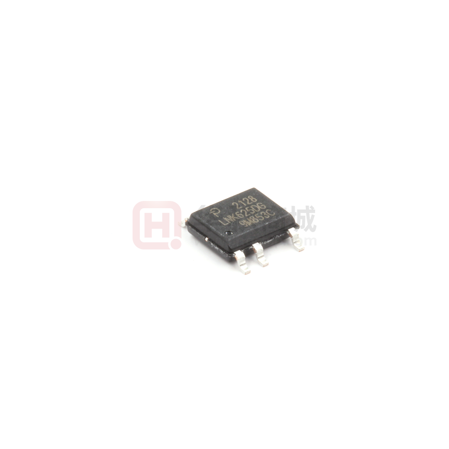
LNK623-626
LinkSwitch-CV Family
Energy-Efficient, Off-line Switcher with Accurate
Primary-side Constant-Voltage (CV) Control
Product Highlights
*
Dramatically Simplifies CV Converters
• Eliminates optocoupler and all secondary CV control circuitry
• Eliminates bias winding supply – IC is self biasing
Advanced Performance Features
• Compensates for external component temperature variations
• Very tight IC parameter tolerances using proprietary trimming
technology
• Continuous and/or discontinuous mode operation for design
flexibility
• Frequency jittering greatly reduces EMI filter cost
• Even tighter output tolerances achievable with external resistor
selection/trimming
Wide Range
High-Voltage
DC Input
output short-circuit and all control loop faults (open and shorted
components)
• Hysteretic thermal shutdown – automatic recovery reduces power
supply returns from the field
• Meets HV creepage requirements between Drain and all other pins,
both on the PCB and at the package
PI-5195-012915
(a) Typical Application Schematic
±5%
VO
70 mW with optional external bias
PI-5196-012315
• Easily meets all global energy efficiency regulations with no added
loads – ideal for mandatory EISA and ENERGY STAR 2.0 regulations
• No primary or secondary current sense resistors – maximizes
efficiency
Green Package
• Halogen free and RoHS compliant package
Applications
•
•
•
•
•
DVD/STB
Adapters
Standby and auxiliary supplies
Home appliances, white goods and consumer electronics
Industrial controls
Description
The LinkSwitchTM-CV dramatically simplifies low power, constant voltage
(CV) converter design through a revolutionary control technique which
eliminates the need for both an optocoupler and secondary CV control
circuitry while providing very tight output voltage regulation. The
combination of proprietary IC trimming and E-Shield™ transformer
construction techniques enables Clampless™ designs with the
LinkSwitch-CV LNK623/4.
LinkSwitch-CV provides excellent cross-regulation for multiple-output
flyback applications such as DVDs and STBs. A 725 V power MOSFET
and ON/OFF control state machine, self-biasing, frequency jittering,
cycle-by-cycle current limit, and hysteretic thermal shutdown circuitry
are all incorporated onto one IC.
art
st
Re
toAu
• No-load consumption 95% for
D
IO
(b) Output Characteristic
Figure 1. Typical Application Schematic (a) and Output Characteristic Envelope
(b). *Optional with LNK623-624PG/DG. (see Key Application Consider-
ations section for clamp and other external circuit design considerations).
Output Power Table
230 VAC ±15%
85-265 VAC
Adapter1
Peak or
Open
Frame2
Adapter1
Peak or
Open
Frame2
LNK623PG/DG
6.5 W
9W
5.0 W
6W
LNK624PG/DG
7W
11 W
5.5 W
6.5 W
LNK625PG/DG
8W
13.5 W
6.5 W
8W
LNK626PG/DG
10.5 W
17 W
8.5 W
10 W
Product
3
Table 1. Output Power Table. Based on 5 V Output.
Notes:
1. Minimum continuous power in a typical non-ventilated enclosed adapter
measured at +50 °C ambient.
2. Maximum practical continuous power in an open frame design with adequate
heat sinking, measured at 50 °C ambient (see Key Application Considerations
section for more information).
3. Packages: P: DIP-8C, D: SO-8C.
Figure 2. DIP-8C P and SO-8C D Packages.
www.power.com
August 2015
This Product is Covered by Patents and/or Pending Patent Applications.
�LNK623-626
REGULATOR
6V
BYPASS
(BP)
FEEDBACK
(FB)
DRAIN
(D)
+
+
VTH
D
-
Q
FB
OUT
STATE
MACHINE
Reset
-
VILIMIT
tSAMPLE-OUT
ILIM
6V
5V
Drive
DCMAX
6.5 V
FAULT
Auto-Restart
Open-Loop
FB
THERMAL
SHUTDOWN
DCMAX
tSAMPLE-OUT
SAMPLE
DELAY
OSCILLATOR
SOURCE
(S)
+
SOURCE
(S)
ILIM
-
Current Limit
Comparator
VILIMIT
LEADING
EDGE
BLANKING
PI-5197-012915
Figure 3
Functional Block Diagram.
Pin Functional Description
DRAIN (D) Pin:
This pin is the power MOSFET drain connection. It provides internal
operating current for both start-up and steady-state operation.
BYPASS (BP) Pin:
This pin is the connection point for an external bypass capacitor for
the internally generated 6 V supply.
FEEDBACK (FB) Pin:
During normal operation, switching of the power MOSFET is
controlled by this pin. This pin senses the AC voltage on the bias
winding. This control input regulates the output voltage based on the
flyback voltage of the bias winding.
P Package (DIP-8C)
FB
BP
1
2
8
7
6
D
4
5
SOURCE (S) Pin:
This pin is internally connected to the output MOSFET source for
high-voltage power and control circuit common returns.
S
S
D Package (SO-8C)
FB
BP
8
2
7
6
S
S
1
D
4
5
S
S
S
S
PI-5198-012315
Figure 4. Pin Configuration.
2
Rev. H 08/15
www.power.com
�LNK623-626
LinkSwitch-CV Functional Description
The LinkSwitch-CV combines a high-voltage power MOSFET switch
with a power supply controller in one device. Similar to the
LinkSwitch-LP and TinySwitch-III it uses ON/OFF control to regulate
the output voltage. The LinkSwitch-CV controller consists of an
oscillator, feedback (sense and logic) circuit, 6 V regulator, overtemperature protection, frequency jittering, current limit circuit,
leading-edge blanking, and ON/OFF state machine for CV control.
Constant Voltage (CV) Operation
The controller regulates the FEEDBACK pin voltage to remain at VFBth
using an ON/OFF state-machine. The FEEDBACK pin voltage is
sampled 2.5 ms after the turn-off of the high-voltage switch. At light
loads the current limit is also reduced to decrease the transformer
flux density.
Auto-Restart and Open-Loop Protection
In the event of a fault condition such as an output short or an open
loop condition the LinkSwitch-CV enters into an appropriate
protection mode as described below.
In the event the FEEDBACK pin voltage during the Flyback period falls
below VFBth-0.3 V before the FEEDBACK pin sampling delay (~2.5 ms)
for a duration in excess of 200 ms (auto-restart on-time (t AR-ON) the
converter enters into auto-restart, wherein the power MOSFET is
disabled for 2.5 seconds (~8% auto-restart duty cycle). The auto-restart
alternately enables and disables the switching of the power MOSFET
until the fault condition is removed.
In addition to the conditions for auto-restart described above, if the
sensed FEEDBACK pin current during the Forward period of the
conduction cycle (switch “on” time) falls below 120 mA, the converter
annunciates this as an open-loop condition (top resistor in potential
divider is open or missing) and reduces the auto-restart time from
200 ms to approximately 6 clock cycles (90 ms), whilst keeping the
disable period of 2.5 seconds. This effectively reduces the autorestart duty cycle to less than 0.01%.
Over-Temperature Protection
The thermal shutdown circuitry senses the die temperature. The
threshold is set at 142 °C typical with a 60 °C hysteresis. When the
die temperature rises above this threshold (142 °C) the power
MOSFET is disabled and remains disabled until the die temperature
falls by 60 °C, at which point the MOSFET is re-enabled.
Current Limit
The current limit circuit senses the current in the power MOSFET.
When this current exceeds the internal threshold (ILIMIT), the power
MOSFET is turned off for the remainder of that cycle. The leading
edge blanking circuit inhibits the current limit comparator for a short
time (tLEB) after the power MOSFET is turned on. This leading edge
blanking time has been set so that current spikes caused by
capacitance and rectifier reverse recovery time will not cause
premature termination of the MOSFET conduction.
6.0 V Regulator
The 6 V regulator charges the bypass capacitor connected to the
BYPASS pin to 6 V by drawing a current from the voltage on the
DRAIN, whenever the MOSFET is off. The BYPASS pin is the internal
supply voltage node. When the MOSFET is on, the device runs off of
the energy stored in the bypass capacitor. Extremely low power
consumption of the internal circuitry allows the LinkSwitch-CV to
operate continuously from the current drawn from the DRAIN pin.
A bypass capacitor value of 1 mF is sufficient for both high frequency
decoupling and energy storage.
3
www.power.com
Rev. H 08/15
�LNK623-626
Applications Example
L1
3.5 × 7.6 mm
Ferrite Bead
1
R1
5.1 kΩ
1/8 W
D1
FR106
D2
FR106
C3
820 pF
1 kV
VR1
1N5272B
T1
EEL19
3
D8
UF4003
6
F1
3.15 A
D7 SB540
11
R2
390 Ω
RV1
275 V
N
12
C1
22 µF
400 V
C2
22 µF
400 V
4
RT1
10 Ω
D4
1N4007
D
C8
1000 µF
10 V
C11
47 µF
50 V
D9
UF4003
C10
470 µF
10 V
R9
39 kΩ
1/8 W
5 V, 1.7 A
R7
510 Ω
1/8 W
RTN
-22 V, 15 mA
D6
1N4148
2
D3
1N4007
C13
270 pF
R10
47 Ω
R8
24 kΩ
1/8 W
L3
10 µH
5
D5
1N4007
85 - 265
VAC
C9
47 µF
25 V
7
8,9,10
L
12 V, 0.1 A
LinkSwitch-CV
U1
LNK626PG
R3
6.34 kΩ
1%
FB
BP
S
L2
680 µH
C4
1 µF
50 V
R4
6.2 kΩ
C5
680 pF
50 V
R5
47 kΩ
1/8 W
R6
4.02 kΩ
1%
C6
10 µF
50 V
PI-5205-012315
Figure 5. 7 W (10 W peak) Multiple Output Flyback Converter for DVD Applications with Primary Sensed Feedback.
Circuit Description
This circuit is configured as a three output, primary-side regulated
flyback power supply utilizing the LNK626PG. It can deliver 7 W
continuously and 10 W peak (thermally limited) from an universal
input voltage range (85 – 265 VAC). Efficiency is >67% at 115
VAC/230 VAC and no-load input power is 5 W, Clampless designs are not practical and
an external RCD or Zener clamp should be used.
4. Ensure that worst-case, high line, peak drain voltage is below the
BVDSS specification of the internal MOSFET and ideally ≤650 V to
allow margin for design variation.
VOR (Reflected Output Voltage), is the secondary output plus output
diode forward voltage drop that is reflected to the primary via the
turns ratio of the transformer during the diode conduction time. The
VOR adds to the DC bus voltage and the leakage spike to determine the
peak drain voltage.
Pulse Grouping
Pulse grouping is defined as 6 or more consecutive pulses followed by
two or more timing state changes. The effect of pulse grouping is
increased output voltage ripple. This is shown on the right of Figure
12 where pulse grouping has caused an increase in the output ripple.
To eliminate group pulsing verify that the feedback signal settles
within 2.1 ms from the turn off of the internal MOSFET. A Zener diode
in the clamp circuit may be needed to achieve the desired settling
time. If the settling time is satisfactory, then a RC network across
RLOWER (R6) of the feedback resistors is necessary.
The value of R (R5 in the Figure 13) should be an order of magnitude
greater than RLOWER and selected such that R×C = 32 ms where C is
C5 in Figure 13.
Quick Design Checklist
As with any power supply design, all LinkSwitch-CV designs should be
verified on the bench to make sure that component specifications are
not exceeded under worst-case conditions. The following minimum
set of tests is strongly recommended:
1. Maximum drain voltage – Verify that peak VDS does not exceed
680 V at highest input voltage and maximum output power.
5
D6
1N4148
4
2
D
R3
6.34 kΩ
1%
LinkSwitch-CV
U1
LNK626PG
FB
BP
S
C4
1 µF
50 V
R4
6.2 kΩ
R5
47 kΩ
R6
1/8 W
4.02 kΩ
C5
1%
680 pF
50 V
C6
10 µF
50 V
PI-5268-110608
Figure 13. RC Network Across RBOTTOM (R6) to Reduce Pulse Grouping.
Top Trace: Drain Waveform (200 V/div)
Bottom Trace: Output Ripple Voltage (50 mV/div)
Figure 12. Not Pulse Grouping (5 Consecutive Switching Cycles).
9
www.power.com
Rev. H 08/15
�LNK623-626
2. Maximum drain current – At maximum ambient temperature,
maximum input voltage and maximum output load, verify drain
current waveforms at start-up for any signs of transformer
saturation and excessive leading edge current spikes. LinkSwitch-CV
has a leading edge blanking time of 215 ns to prevent premature
termination of the ON-cycle. Verify that the leading edge current
spike is below the allowed current limit envelope for the drain
current waveform at the end of the 215 ns blanking period.
3. Thermal check – At maximum output power, both minimum and
maximum input voltage and maximum ambient temperature;
verify that temperature specifications are not exceeded for
LinkSwitch-CV, transformer, output diodes and output capacitors.
Enough thermal margin should be allowed for the part-to-part
variation of the RDS(ON) of LinkSwitch-CV, as specified in the data
sheet. It is recommended that the maximum SOURCE pin
temperature does not exceed 110 °C.
Design Tools
Up-to-date information on design tools can be found at the Power
Integrations web site: www.power.com
10
Rev. H 08/15
www.power.com
�LNK623-626
Absolute Maximum Ratings1,5
DRAIN Voltage .........................................................-0.3 V to 725 V
DRAIN Peak Current: LNK623..................................400 (600) mA4
LNK624..................................400 (600) mA4
LNK625..................................528 (790) mA4
LNK626................................ 720 (1080) mA4
Peak Negative Pulsed DRAIN Current ..................................-100 mA2
Feedback Pin Voltage ................................................... -0.3 V to 9 V
Feedback Pin Current ...........................................................100 mA
BYPASS Pin Voltage ..................................................... -0.3 V to 9 V
BYPASS Pin Current................................................................10 mA
Storage Temperature .................................................-65 °C to 150 °C
Operating Junction Temperature...............................-40 °C to 150 °C
Lead Temperature(3) ............................................................... 260 °C
Notes:
1. All voltages referenced to SOURCE, TA = 25 °C.
2. Duration not to exceed 2 msec.
3. 1/16 in. from case for 5 seconds.
4. The higher peak DRAIN current is allowed while the DRAIN
voltage is simultaneously less than 400 V.
5. Maximum ratings specified may be applied, one at a time
without causing permanent damage to the product.
Exposure to Absolute Maximum ratings for extended
periods of time may affect product reliability.
Thermal Resistance
Thermal Resistance: P Package:
(qJA) ......................................... 70 °C/W2; 60 °C/W3
(qJC)1 ....................................................... 11 °C/W
D Package:
(qJA) ......................................100 °C/W2; 80 °C/W3
(qJC)1........................................................ 30 °C/W
Parameter
Notes:
1. Measured on pin 8 (SOURCE) close to plastic interface.
2. Soldered to 0.36 sq. in. (232 mm2), 2 oz. (610 g/m2) copper clad.
3. Soldered to 1 sq. in. (645 mm2), 2 oz. (610 g/m2) copper clad.
Conditions
SOURCE = 0 V; TJ = -40 to 125 °C
(Unless Otherwise Specified)
Symbol
Min
Typ
Max
Units
93
100
106
kHz
Control Functions
Output Frequency
fOSC
TJ = 25 °C, VFB = VFBth
Frequency Jitter
LNK623/6
Peak-Peak Jitter Compared to
Average Frequency, TJ = 25 °C
±7
%
80
%
Ratio of Output
Frequency at AutoRestart
fOSC(AR)
TJ = 25 °C
Relative to fOSC , See Note C
Maximum Duty Cycle
DCMAX
TJ = 25 °C
See Notes B, C
FEEDBACK Pin Voltage
TJ = 25 °C
See Figure 15
CBP = 1 mF
See Note D
VFBth
54
%
LNK623-624P
1.815
1.840
1.865
LNK623-624D
1.855
1.880
1.905
LNK625P, LNK625D
1.835
1.860
1.885
LNK626P, LNK626D
1.775
1.800
1.825
V
FEEDBACK Pin
Voltage Temperature
Coefficient
TC VFB
-0.01
%/°C
FEEDBACK Pin Voltage
at Turn-Off Threshold
VFB(AR)
1.45
V
Power Coefficient
I2f = I2LIMIT(TYP) × fOSC(TYP)
LNK623/6P
TJ = 25 °C
0.9 × I2f
I2 f
1.17 × I2f
If=I
LNK623/6D
TJ = 25 °C
0.9 × I f
If
1.21 × I f
I2 f
2
2
LIMIT(TYP)
× fOSC(TYP)
A2Hz
2
2
2
11
www.power.com
Rev. H 08/15
�LNK623-626
Symbol
Conditions
SOURCE = 0 V; TJ = -40 to 125 °C
(Unless Otherwise Specified)
Minimum Switch
“On”-Time
tON(min)
See Note C
FEEDBACK Pin
Sampling Delay
tFB
Parameter
Min
Typ
Max
Units
Control Functions (cont.)
DRAIN Supply
Current
700
2.35
IS1
FB Voltage > VFBth
IS2
FB Voltage = VFBth -0.1,
Switch ON-Time = tON (MOSFET
Switching at fOSC)
ICH1
VBP = 0 V
BYPASS Pin
Charge Current
ICH2
VBP = 4 V
ns
2.55
2.75
280
330
LNK623/4
440
520
LNK625
480
560
LNK626
520
600
LNK623/4
-5.0
-3.4
-1.8
LNK625/6
-7.0
-4.5
-2.0
LNK623/4
-4.0
-2.3
-1.0
LNK625/6
-5.6
-3.2
-1.4
ms
mA
mA
BYPASS Pin Voltage
VBP
5.65
6.00
6.25
V
BYPASS Pin
Voltage Hysteresis
VBPH
0.70
1.00
1.20
V
VSHUNT
6.2
6.5
6.8
V
LNK623
di/dt = 50 mA/ms , TJ = 25 °C
196
210
225
LNK624
di/dt = 60 mA/ms , TJ = 25 °C
233
250
268
LNK625
di/dt = 80 mA/ms , TJ = 25 °C
307
330
353
LNK626
di/dt = 110 mA/ms , TJ = 25 °C
419
450
482
TJ = 25 °C
See Note C
170
215
135
142
BYPASS Pin
Shunt Voltage
Circuit Protection
Current Limit
ILIMIT
Leading Edge
Blanking Time
tLEB
Thermal Shutdown
Temperature
TSD
Thermal Shutdown
Hysteresis
TSDH
mA
60
ns
150
°C
°C
12
Rev. H 08/15
www.power.com
�LNK623-626
Parameter
Symbol
Conditions
SOURCE = 0 V; TJ = -40 to 125 °C
(Unless Otherwise Specified)
Min
Typ
Max
TJ = 25 °C
24
28
TJ = 100 °C
36
42
TJ = 25 °C
24
28
TJ = 100 °C
36
42
TJ = 25 °C
16
19
TJ = 100 °C
24
28
TJ = 25 °C
9.6
11
TJ = 100 °C
14
17
Units
Output
LNK623
ID = 50 mA
ON-State
Resistance
LNK624
ID = 50 mA
RDS(ON)
LNK625
ID = 62 mA
LNK626
ID = 82 mA
OFF-State
Leakage
IDSS1
IDSS2
Breakdown
Voltage
BVDSS
VDS = 560 V, See Figure 20
t AR-ON
Auto-Restart
OFF-Time
t AR-OFF
Open-Loop
FEEDBACK Pin
Current Threshold
IOL
Open-Loop
ON-Time
mA
VDS = 375 V, See Figure 20
15
TJ = 50 °C
DRAIN Supply
Voltage
Auto-Restart
ON-Time
50
TJ = 125 °C, See Note A
TJ = 25 °C
See Figure 20
VFB = 0
See Note C
W
725
V
50
V
200
ms
LNK623/624/626
2
s
LNK625
1
See Note C
-120
mA
See Note C
90
ms
NOTES:
A. IDSS1 is the worst-case OFF-state leakage specification at 80% of BVDSS and maximum operating junction temperature. IDSS2 is a typical
specification under worst-case application conditions (rectified 265 VAC) for no-load consumption calculations.
B. When the duty cycle exceeds DCMAX the LinkSwitch-CV operates in on-time extension mode.
C. This parameter is derived from characterization.
D. Mechanical stress induced during the assembly may cause shift in this parameter. This shift has not impact on the ability of LinkSwitch-CV
to meet CV = ±5% in mass production given the design follows recommendation in AN-45 and good manufacturing practice.
13
www.power.com
Rev. H 08/15
�LNK623-626
Typical Performance Characteristics
Feedback Voltage
(Normalized to 25 °C)
1.000
0.800
0.600
0.400
0.200
10
35
60
85
0.800
0.600
0.400
0.200
0.000
-40
110 135
-15
Figure 14. Output Frequency vs. Temperature.
1.0
300
Drain Current (mA)
PI-2213-012315
Breakdown Voltage
(Normalized to 25 °C)
35
250
25
50
150
100
Scaling Factors:
LNK623
1.0
LNK624
1.0
LNK625
1.5
LNK626
2.5
0
75 100 125 150
2
4
6
8
10
DRAIN Voltage (V)
Junction Temperature (°C)
Figure 17. Output Characteristic.
Scaling Factors:
LNK623
1.0
LNK624
1.0
LNK625
1.5
LNK626
2.5
50
PI-5201-012615
Figure 16. Breakdown vs. Temperature.
1000
110 135
200
0
0
85
TCASE=25 °C
TCASE=100 °C
50
0.9
-50 -25
60
Figure 15. Feedback Voltage vs. Temperature.
1.1
100
10
Scaling Factors:
LNK623
1.0
LNK624
1.0
LNK625
1.5
LNK626
2.5
40
Power (mW)
Drain Capacitance (pF)
10
Temperature (°C)
Temperature (°C)
PI-5211-080708
-15
1.000
PI-5212-012615
0.000
-40
PI-5089-012315
1.200
PI-5086-012315
Frequency
(Normalized to 25 °C)
1.200
30
20
10
0
1
0
100
200
300
400
Drain Voltage (V)
Figure 18. COSS vs. Drain Voltage.
500
600
0
200
400
600
DRAIN Voltage (V)
Figure 19. Drain Capacitance Power.
14
Rev. H 08/15
www.power.com
�LNK623-626
LinkSwitch-CV
5 µF
50 kΩ
10 kΩ
1 µF
FB
S
BP
S
D
S
.1 µF
4 kΩ
VIN
16 V
S1
S
S2
+
Curve
Tracer
To measure BVDSS, IDSS1, and IDSS2 follow these steps:
1) Close S1, open S2
2) Power-up VIN source (16 V)
3) Open S1, close S2
4) Measure I/V characteristics of DRAIN pin using the curve tracer
PI-5203-012615
Figure 20. Test Set-up for Leakage and Breakdown Tests.
15
www.power.com
Rev. H 08/15
�LNK623-626
PDIP-8C (P Package)
-E-
⊕ D S .004 (.10)
.240 (6.10)
.260 (6.60)
Pin 1
-D-
.367 (9.32)
.387 (9.83)
.057 (1.45)
.068 (1.73)
(NOTE 6)
.125 (3.18)
.145 (3.68)
-T-
Notes:
1. Package dimensions conform to JEDEC specification
MS-001-AB (Issue B 7/85) for standard dual-in-line (DIP)
package with .300 inch row spacing.
2. Controlling dimensions are inches. Millimeter sizes are
shown in parentheses.
3. Dimensions shown do not include mold flash or other
protrusions. Mold flash or protrusions shall not exceed
.006 (.15) on any side.
4. Pin locations start with Pin 1, and continue counter-clockwise to Pin 8 when viewed from the top. The notch and/or
dimple are aids in locating Pin 1. Pin 3 is omitted.
5. Minimum metal to metal spacing at the package body for
the omitted lead location is .137 inch (3.48 mm).
6. Lead width measured at package body.
7. Lead spacing measured with the leads constrained to be
perpendicular to plane T.
.015 (.38)
MINIMUM
SEATING
PLANE
.120 (3.05)
.140 (3.56)
.100 (2.54) BSC
.014 (.36)
.022 (.56)
.048 (1.22)
.053 (1.35)
⊕T
.137 (3.48)
MINIMUM
E D S .010 (.25) M
.008 (.20)
.015 (.38)
.300 (7.62) BSC
(NOTE 7)
.300 (7.62)
.390 (9.91)
P08C
PI-3933-012315
16
Rev. H 08/15
www.power.com
�LNK623-626
SO-8C (D Package)
4
B
0.10 (0.004) C A-B 2X
2
DETAIL A
4.90 (0.193) BSC
A
4
8
D
5
2 3.90 (0.154) BSC
GAUGE
PLANE
SEATING
PLANE
6.00 (0.236) BSC
o
0-8
C
0.25 (0.010)
BSC
1.04 (0.041) REF
2X
0.10 (0.004) C D
1
Pin 1 ID
4
2X
7X 0.31 - 0.51 (0.012 - 0.020)
0.25 (0.010) M C A-B D
1.27 (0.050) BSC
1.35 (0.053)
1.75 (0.069)
0.40 (0.016)
1.27 (0.050)
0.20 (0.008) C
1.25 - 1.65
(0.049 - 0.065)
DETAIL A
0.10 (0.004)
0.25 (0.010)
0.10 (0.004) C
H
7X
SEATING PLANE
0.17 (0.007)
0.25 (0.010)
C
Reference
Solder Pad
Dimensions
+
2.00 (0.079)
+
4.90 (0.193)
+
+
1.27 (0.050)
D07C
Notes:
1. JEDEC reference: MS-012.
2. Package outline exclusive of mold flash and metal burr.
3. Package outline inclusive of plating thickness.
4. Datums A and B to be determined at datum plane H.
5. Controlling dimensions are in millimeters. Inch dimensions
are shown in parenthesis. Angles in degrees.
0.60 (0.024)
PI-4526-012315
Part Ordering Information
• LinkSwitch Product Family
• CV Series Number
• Package Identifier
P
Plastic DIP
D
Plastic SO-8
• Package Material
G
GREEN: Halogen Free and RoHS Compliant
• Tape & Reel and Other Options
Blank
LNK 625 D G - TL
TL
Standard Configurations
Tape & Reel, 2.5 k pcs for D Package. Not available for P Package.
17
www.power.com
Rev. H 08/15
�Revision
Notes
Date
B
C
Release data sheet.
Correction made to Figure 5.
11/08
12/08
D
Introduced Max Current Limit when V DRAIN is below 400 V.
07/09
E
Introduced LNK626DG.
09/09
F
Added Note 4 to Parameter Table
02/10
F
Specified Max BYPASS Pin Current.
03/14
G
Figure removed “Test Set-up for FEEDBACK Pin Measurements” from previous version. Updated t AR-OFF parameter.
Updated to latest Brand Style.
02/15
H
Update BVDSS from 700 V to 725 V
08/15
For the latest updates, visit our website: www.power.com
Power Integrations reserves the right to make changes to its products at any time to improve reliability or manufacturability. Power Integrations
does not assume any liability arising from the use of any device or circuit described herein. POWER INTEGRATIONS MAKES NO WARRANTY
HEREIN AND SPECIFICALLY DISCLAIMS ALL WARRANTIES INCLUDING, WITHOUT LIMITATION, THE IMPLIED WARRANTIES OF MERCHANTABILITY,
FITNESS FOR A PARTICULAR PURPOSE, AND NON-INFRINGEMENT OF THIRD PARTY RIGHTS.
Patent Information
The products and applications illustrated herein (including transformer construction and circuits external to the products) may be covered by one
or more U.S. and foreign patents, or potentially by pending U.S. and foreign patent applications assigned to Power Integrations. A complete list of
Power Integrations patents may be found at www.power.com. Power Integrations grants its customers a license under certain patent rights as set
forth at http://www.power.com/ip.htm.
Life Support Policy
POWER INTEGRATIONS PRODUCTS ARE NOT AUTHORIZED FOR USE AS CRITICAL COMPONENTS IN LIFE SUPPORT DEVICES OR SYSTEMS
WITHOUT THE EXPRESS WRITTEN APPROVAL OF THE PRESIDENT OF POWER INTEGRATIONS. As used herein:
1. A Life support device or system is one which, (i) is intended for surgical implant into the body, or (ii) supports or sustains life, and (iii) whose
failure to perform, when properly used in accordance with instructions for use, can be reasonably expected to result in significant injury or
death to the user.
2. A critical component is any component of a life support device or system whose failure to perform can be reasonably expected to cause the
failure of the life support device or system, or to affect its safety or effectiveness.
The PI logo, TOPSwitch, TinySwitch, LinkSwitch, LYTSwitch, InnoSwitch, DPA-Switch, PeakSwitch, CAPZero, SENZero, LinkZero, HiperPFS,
HiperTFS, HiperLCS, Qspeed, EcoSmart, Clampless, E-Shield, Filterfuse, FluxLink, StakFET, PI Expert and PI FACTS are trademarks of Power
Integrations, Inc. Other trademarks are property of their respective companies. ©2015, Power Integrations, Inc.
Power Integrations Worldwide Sales Support Locations
World Headquarters
5245 Hellyer Avenue
San Jose, CA 95138, USA.
Main: +1-408-414-9200
Customer Service:
Phone: +1-408-414-9665
Fax: +1-408-414-9765
e-mail: usasales@power.com
China (Shanghai)
Rm 2410, Charity Plaza, No. 88
North Caoxi Road
Shanghai, PRC 200030
Phone: +86-21-6354-6323
Fax: +86-21-6354-6325
e-mail: chinasales@power.com
China (Shenzhen)
17/F, Hivac Building, No. 2, Keji Nan
8th Road, Nanshan District,
Shenzhen, China, 518057
Phone: +86-755-8672-8689
Fax: +86-755-8672-8690
e-mail: chinasales@power.com
Germany
Lindwurmstrasse 114
80337 Munich
Germany
Phone: +49-895-527-39110
Fax: +49-895-527-39200
e-mail: eurosales@power.com
India
#1, 14th Main Road
Vasanthanagar
Bangalore-560052 India
Phone: +91-80-4113-8020
Fax: +91-80-4113-8023
e-mail: indiasales@power.com
Italy
Via Milanese 20, 3rd. Fl.
20099 Sesto San Giovanni (MI)
Italy
Phone: +39-024-550-8701
Fax: +39-028-928-6009
e-mail: eurosales@power.com
Japan
Kosei Dai-3 Bldg.
2-12-11, Shin-Yokohama,
Kohoku-ku
Yokohama-shi Kanagwan
222-0033 Japan
Phone: +81-45-471-1021
Fax: +81-45-471-3717
e-mail: japansales@power.com
Taiwan
5F, No. 318, Nei Hu Rd., Sec. 1
Nei Hu Dist.
Taipei 11493, Taiwan R.O.C.
Phone: +886-2-2659-4570
Fax: +886-2-2659-4550
e-mail: taiwansales@power.com
UK
Cambridge Semiconductor,
Korea
a Power Integrations company
RM 602, 6FL
Westbrook Centre, Block 5, 2nd Floor
Korea City Air Terminal B/D, 159-6 Milton Road
Samsung-Dong, Kangnam-Gu,
Cambridge CB4 1YG
Seoul, 135-728, Korea
Phone: +44 (0) 1223-446483
Phone: +82-2-2016-6610
e-mail: eurosales@power.com
Fax: +82-2-2016-6630
e-mail: koreasales@power.com
Singapore
51 Newton Road
#19-01/05 Goldhill Plaza
Singapore, 308900
Phone: +65-6358-2160
Fax: +65-6358-2015
e-mail: singaporesales@power.com
�