LQA30A300C Qspeed™ Family
300 V, 30 A Q-Series Common-Cathode Diode
Product Summary
IF(AVG) per diode VRRM QRR (Typ at 125 °C) IRRM (Typ at 125 °C) Softness tb/ta (Typ at 125 °C) 15 300 47 2.7 0.7 A V nC A
General Description
This device has the lowest QRR of any 300V Silicon diode. Its recovery characteristics increase efficiency, reduce EMI and eliminate snubbers.
Applications Pin Assignment
• AC/DC and DC/DC output rectification • Output & freewheeling diodes • Motor drive circuits • DC-AC inverters
A1 A1 K A2
Features
K (Backside Heatsink)
• Low QRR, Low IRRM, Low tRR • High dIF/dt capable (1000A/µs) • Soft recovery
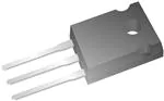
TO-247 AD
A1 A2 K
Benefits
• Increases efficiency • Eliminates need for snubber circuits • Reduces EMI filter component size & count • Enables extremely fast switching
RoHS Compliant
Package uses Lead-free plating and Green mold compound Halogen free per IEC 61249-2-21.
Absolute Maximum Ratings
Absolute maximum ratings are the values beyond which the device may be damaged or have its useful life impaired. Functional operation under these conditions is not implied.
Symbol
VRRM IF(AVG) IFSM IFSM TJ TSTG PD
Parameter
Peak repetitive reverse voltage Average forward current Non-repetitive peak surge current Non-repetitive peak surge current Maximum junction temperature Storage temperature Lead soldering temperature Power dissipation
Conditions
Per Diode, TJ = 150 °C, TC = 108 °C Per Device, TJ = 150 °C, TC = 108 °C Per Diode, 60 Hz, ½ cycle Per Diode, ½ cycle of t = 28 µs Sinusoid, TC = 25 °C
Rating
300 15 30 100 350 150 –55 to 150 300 65.8
Units
V A A A A °C °C °C W
Leads at 1.6mm from case, 10 sec TC = 25 °C
Thermal Resistance
Symbol
RθJA RθJC
Resistance from:
Junction to ambient Junction to case
Conditions
Per Device Per Diode Per Device
Rating
40 (Typ) 1.9 0.95
Units
°C/W °C/W °C/W
www.powerint.com
January 2011
�LQA30A300C
Electrical Specifications at TJ= 25 °C (unless otherwise specified)
Symbol
IR VF CJ
Parameter
Reverse current per diode Forward voltage per diode Junction capacitance per diode Reverse recovery time, per diode Reverse recovery charge, per diode Maximum reverse recovery current, per diode
Conditions
VR = 300 V, TJ = 25 °C VR = 300 V, TJ = 125 °C IF = 15 A, TJ = 25 °C IF = 15 A, TJ = 150 °C VR = 10 V, 1 MHz
Min
-
Typ
0.45 1.6 1.4 50
Max
25 1.9 -
Units
µA mA V V pF
DC Characteristics
Dynamic Characteristics
tRR QRR IRRM dIF/dt =200 A/µs VR=200, IF=15 A dIF/dt =200 A/µs VR=200, IF=15 A dIF/dt =200 A/µs VR=200, IF=15 A dIF/dt =200 A/µs VR=200, IF=15 A TJ=25 °C TJ=125 °C TJ=25 °C TJ =125 °C TJ =25 °C TJ=125 °C TJ =25 °C TJ=125 °C 13 26 12.5 47 1.5 2.7 0.7 0.7 16 1.9 ns ns nC nC A A
S
t Softness per diode= b
ta
Note to component engineers: Q-Series diodes employ Schottky technologies in their design and construction. Therefore, component engineers should plan their test setups to be similar to traditional Schottky test setups. (For further details, see application note AN-300.)
VR
L1
D1 DUT
IF dIF/dt
0
tRR ta tb 0.1xIRRM IRRM
15V
Pulse generator
+
Rg Q1
Figure 1. Reverse Recovery Definitions
Figure 2. Reverse Recovery Test Circuit
2
www.powerint.com
Rev 1.1 01/11
�LQA30A300C
Electrical Specifications at TJ= 25 °C (unless otherwise specified)
50 45 40 35 30 25 20 15 10 5 0 0.0 0.5 1.0 VF (V) 1.5 2.0 2.5 Tj=25C Tj=125C
IF ( A)
1.0 0.9 0.8 0.7 0.6 0.5 0.4 0.3 0.2 0.1 0.0 0.0 0.1 0.2 0.3 0.4 0.5 VF (V) 0.6 0.7 0.8 0.9 1.0 Tj=25C Tj=125C
IF ( A)
Figure 3. Typical IF vs VF
Figure 4. Typical IF vs VF
200 180 160 IF(A V) ( A) 140 120 100 80 60 40 20 0 0 20 40 60 80 100 120 140 160 180 VR (V)
40 35 30 25 20 15 10 5 0 25 50 75 100
o
C j ( pF)
125
150
Case Temperature, TC ( C)
Figure 5. Typical Cj vs VR
Figure 6. DC Current Derating Curve
100 90 80 Q R R (n C)
tR R (ns)
30
dI/dt=200A/us
dI/dt=500A/us
25
70 60 50 40 30 20 0 5 10 IF (A) 15 20 25 dI/dt=200A/us
20 dI/dt=500A/us 15
10 0 5 10 IF (A) 15 20 25
Figure 7. Typical QRR vs IF at Tj=125 °C
Figure 8. Typical tRR vs IF at Tj=125 °C
3
Rev 1.1 01/11
www.powerint.com
�LQA30A300C
80 70 60 50 P (W) 40 30 20 10 0 25 50 75 100
o
125
150
60 55 50 45 40 35 30 25 20 15 10 5 0 25 50 75 100 T C(°C) 125
duty cycle=10% duty cycle=30% duty cycle=50% DC
IF(PEAK) (A)
Case Temperature, TC ( C)
150
Figure 9. Power Derating Curve
Figure 10. IF(Peak) vs TC, f=70 kHz
LQA30A300C
1
D= 0.5 D = 0.3
0.1 Zth(j-c)/Rth(j-c)
D= 0.1
D= 0.05
D= 0.02
D= 0.01
0.01
D= 0.005
D= 0.002
Single Pulse
0.001 1.E-06
1.E-05
1.E-04
1.E-03 t1(sec)
1.E-02
1.E-01
1.E+00
Figure 11. Normalized Maximum Transient Thermal Impedance
4
www.powerint.com
Rev 1.1 01/11
�LQA30A300C
Dimensional Outline Drawings
TO-247 AD
Dim A A1 A2 b b2 b4 c D D1 D2 E E1 E2 E3 e L L1 ØP ØP1 ØP2 Q S T U 9.80 6.00
Millimeters
MIN 4.90 2.31 1.90 1.16 1.96 2.96 0.59 20.90 16.25 1.05 15.70 13.10 4.90 2.40 5.44BSC 19.80 3.50 2.40 5.60 6.15BSC 10.20 6.40 21.10 4.30 3.70 7.40 2.60 6.00 MAX 5.10 2.51 2.10 1.26 2.06 3.06 0.66 21.10 16.85 1.35 15.90 13.50 5.10 2.60
Mechanical Mounting Method
Screw through hole in package tab Clamp against package body
Maximum Torque / Pressure specification
1 Newton Meter (nm) or 8.8 inch-pounds (lb-in) 12.3 kilogram-force per square centimeter (kgf/cm2) or 175 lbf/in2
Soldering time and temperature: This product has been designed for use with high-temperature, leadfree solder. The component leads can be subjected to a maximum temperature of 300 °C, for up to 10 seconds. See Application Note AN-303, for more details.
Ordering Information
Part Number
LQA30A300C
Package
TO-247
Packing
30 units/tube
The information contained in this document is subject to change without notice.
5
Rev 1.1 01/11
www.powerint.com
�LQA30A300C
Revision 1.0 1.1
Notes Released by Qspeed Converted to Power Integrations Document
Date 08/09 01/11
6
www.powerint.com
Rev 1.1 01/11
�LQA30A300C
For the latest updates, visit our website: www.powerint.com
Power Integrations reserves the right to make changes to its products at any time to improve reliability or manufacturability. Power Integrations does not assume any liability arising from the use of any device or circuit described herein. POWER INTEGRATIONS MAKES NO WARRANTY HEREIN AND SPECIFICALLY DISCLAIMS ALL WARRANTIES INCLUDING, WITHOUT LIMITATION, THE IMPLIED WARRANTIES OF MERCHANTABILITY, FITNESS FOR A PARTICULAR PURPOSE, AND NON-INFRINGEMENT OF THIRD PARTY RIGHTS. PATENT INFORMATION The products and applications illustrated herein (including transformer construction and circuits external to the products) may be covered by one or more U.S. and foreign patents, or potentially by pending U.S. and foreign patent applications assigned to Power Integrations. A complete list of Power Integrations’ patents may be found at www.powerint.com. Power Integrations grants its customers a license under certain patent rights as set forth at http://www.powerint.com/ip.htm. The PI Logo, TOPSwitch, TinySwitch, LinkSwitch, DPA-Switch, PeakSwitch, CAPZero, SENZero, LinkZero, HiperPFS, HiperTFS, Qspeed, EcoSmart, Clampless, E-Shield, Filterfuse, StackFET, PI Expert and PI FACTS are trademarks of Power Integrations, Inc. Other trademarks are property of their respective companies. ©Copyright 2011 Power Integrations, Inc.
Power Integrations Worldwide Sales Support Locations
WORLD HEADQUARTERS 5245 Hellyer Avenue San Jose, CA 95138, USA. Main: +1-408-414-9200 Customer Service: Phone: +1-408-414-9665 Fax: +1-408-414-9765 e-mail: usasales@powerint.com CHINA (SHANGHAI) Rm 1601/1610, Tower 1 Kerry Everbright City No. 218 Tianmu Road West Shanghai, P.R.C. 200070 Phone: +86-021-6354-6323 Fax: +86-021-6354-6325 e-mail: chinasales@powerint.com CHINA (SHENZHEN) th Rm A, B & C 4 Floor, Block C, Electronics Science and Technology Building 2070 Shennan Zhong Road Shenzhen, Guangdong, P.R.C. 518031 Phone: +86-755-8379-3243 Fax: +86-755-8379-5828 e-mail: chinasales@powerint.com GERMANY Rueckertstrasse 3 D-80336, Munich Germany Phone: +49-89-5527-3911 Fax: +49-89-5527-3920 e-mail: eurosales@powerint.com JAPAN Kosei Dai-3 Building 2-12-11, Shin-Yokohama, Kohoku-ku, Yokohama-shi, Kanagawa 222-0033 Japan Phone: +81-45-471-1021 Fax: +81-45-471-3717 e-mail: japansales@powerint.com KOREA RM 602, 6FL Korea City Air Terminal B/D, 159-6 Samsung-Dong, Kangnam-Gu, Seoul, 135-728 Korea Phone: +82-2-2016-6610 Fax: +82-2-2016-6630 e-mail: koreasales@powerint.com SINGAPORE 51 Newton Road, #19-01/05 Goldhill Plaza Singapore, 308900 Phone: +65-6358-2160 Fax: +65-6358-2015 e-mail: singaporesales@powerint.com TAIWAN 5F, No. 318, Nei Hu Rd., Sec. 1 Nei Hu District Taipei 114, Taiwan R.O.C. Phone: +886-2-2659-4570 Fax: +886-2-2659-4550 e-mail: taiwansales@powerint.com
INDIA th #1, 14 Main Road Vasanthanagar Bangalore-560052 India Phone: +91-80-4113-8020 Fax: +91-80-4113-8023 e-mail: indiasales@powerint.com ITALY Via De Amicis 2 20091 Bresso MI Italy Phone: +39-028-928-6000 Fax: +39-028-928-6009 e-mail: eurosales@powerint.com
EUROPE HQ 1st Floor, St. James’s House East Street, Farnham Surrey GU9 7TJ United Kingdom Phone: +44 (0) 1252-730-141 Fax: +44 (0) 1252-727-689 e-mail: eurosales@powerint.com APPLICATIONS HOTLINE World Wide +1-408-414-9660 APPLICATIONS FAX World Wide +1-408-414-9760
7
Rev 1.1 01/11
www.powerint.com
�