Title
Reference Design Report for a 7.5 W
Continuous, 13 W Peak DVD / Set Top Box
Using TNY376PN
Specification
85–265 VAC Input, 3.3 V (500 mA), 5 V (500 mA),
12 V (250 mA) and –12 V (30 mA) Outputs
Application
DVD / Set Top Box
Author
Power Integrations Applications Department
Document
Number
RDR-115
Date
May 22, 2007
Revision
1.0
Summary and Features
•
•
•
•
•
•
Excellent cross regulation without need for post regulator
EcoSmart® – Meets Energy Star / CEC requirements
• No-load consumption 70% active-mode efficiency
• > 0.5 W output power available for 1 W input simplifies DVD player design
BP/M capacitor value selects MOSFET current limit for greater design flexibility
Tightly toleranced I2f parameter (–10%, +12%) reduces system cost:
• Increases MOSFET and magnetics power delivery
• Reduces overload power, which lowers output diode and capacitor costs
Integrated TinySwitch-PK Safety/Reliability features:
• Accurate (± 5%), auto-recovering, hysteretic thermal shutdown function maintains
safe PCB temperatures under all conditions
• Auto-restart protects against output short circuit and open loop fault
conditions
• > 3.2 mm creepage on package enables reliable operation in high humidity
and high pollution environments
Meets EN550022 and CISPR-22 Class B conducted EMI with >20 dBµV margin
Power Integrations
5245 Hellyer Avenue, San Jose, CA 95138 USA.
Tel: +1 408 414 9200 Fax: +1 408 414 9201
www.powerint.com
�RDR-115 7.5 W, 13 W pk Multi-Output DVD/Set-Top Box Supply
22-May-07
The products and applications illustrated herein (including circuits external to the products and transformer
construction) may be covered by one or more U.S. and foreign patents or potentially by pending U.S. and foreign
patent applications assigned to Power Integrations. A complete list of Power Integrations’ patents may be found at
www.powerint.com.
Power Integrations
Tel: +1 408 414 9200 Fax: +1 408 414 9201
www.powerint.com
Page 2 of 36
�22-May-07
RDR-115 7.5 W, 13 W pk Multi-Output DVD/Set-Top Box Supply
Table of Contents
1
2
3
4
Introduction .................................................................................................................5
Power Supply Specification ........................................................................................6
Schematic ...................................................................................................................7
Circuit Description.......................................................................................................8
4.1
Input EMI Filtering................................................................................................8
4.2
TinySwitch-PK Primary ........................................................................................8
4.3
Output Feedback .................................................................................................9
4.4
Bypass/Multifunction Pin......................................................................................9
5 PCB Layout...............................................................................................................10
6 Bill of Materials .........................................................................................................11
7 Transformer Specification .........................................................................................13
7.1
Electrical Diagram..............................................................................................13
7.2
Electrical Specifications .....................................................................................13
7.3
Materials ............................................................................................................13
7.4
Transformer Build Diagram................................................................................14
7.5
Copper Foil Preparation.....................................................................................14
7.6
Transformer Construction ..................................................................................15
8 Design Spreadsheet .................................................................................................16
9 Performance Data.....................................................................................................18
9.1
Efficiency ...........................................................................................................18
9.1.1
Active Mode CEC Measurement Data........................................................18
9.2
No-load Input Power ..........................................................................................19
9.3
Available Standby Output Power .......................................................................20
9.4
Regulation .........................................................................................................21
9.4.1
Load Regulation, Room Temperature, 115 VAC input. ..............................21
9.4.2
Line.............................................................................................................23
10
Thermal Performance............................................................................................24
11
Waveforms ............................................................................................................25
11.1 Drain Voltage and Current, Normal Operation...................................................25
11.2 Output Voltage Start-up Profile ..........................................................................25
11.3 Drain Voltage and Current Start-up Profile ........................................................26
11.4 Load Transient Response..................................................................................26
11.5 Output Ripple Measurements ............................................................................29
11.5.1 Ripple Measurement Technique.................................................................29
11.5.2 Measurement Results.................................................................................30
11.6 Line Surge .........................................................................................................31
12
Conducted EMI .....................................................................................................32
13
Appendix A............................................................................................................33
13.1 Output Power Delivery Using a TNY375P .........................................................33
14
Revision History ....................................................................................................34
Page 3 of 36
Power Integrations
Tel: +1 408 414 9200 Fax: +1 408 414 9201
www.powerint.com
�RDR-115 7.5 W, 13 W pk Multi-Output DVD/Set-Top Box Supply
22-May-07
Important Note:
Although this board is designed to satisfy safety isolation requirements, the engineering
prototype has not been agency approved. Therefore, all testing should be performed
using an isolation transformer to provide the AC input to the prototype board.
Power Integrations
Tel: +1 408 414 9200 Fax: +1 408 414 9201
www.powerint.com
Page 4 of 36
�22-May-07
RDR-115 7.5 W, 13 W pk Multi-Output DVD/Set-Top Box Supply
1 Introduction
This document is an engineering report describing a four output flyback power supply
utilizing a TNY376PN. This power supply is intended as a general purpose evaluation
platform for TinySwitch-PK
The document contains the power supply specification, schematic, bill of materials,
transformer documentation, printed circuit layout, and performance data.
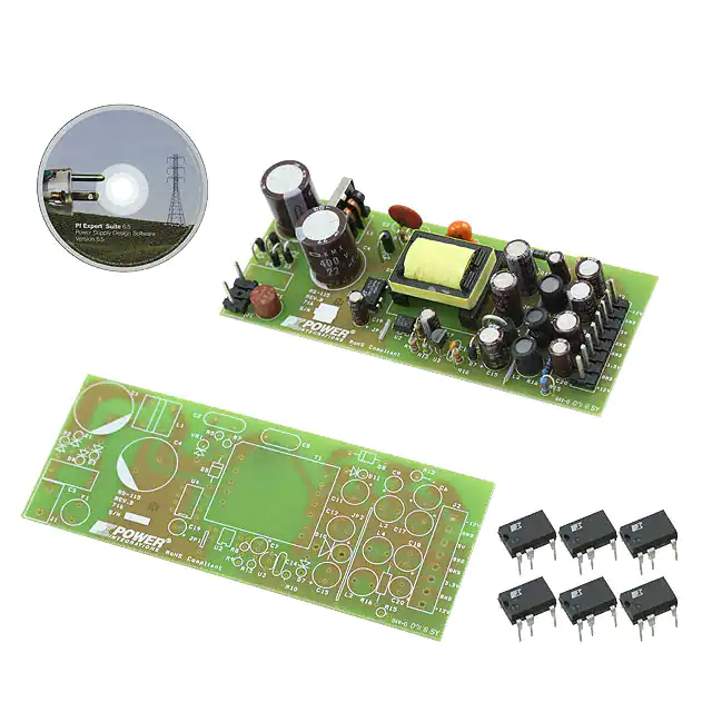
Figure 1 – Populated Circuit Board Photograph.
Page 5 of 36
Power Integrations
Tel: +1 408 414 9200 Fax: +1 408 414 9201
www.powerint.com
�RDR-115 7.5 W, 13 W pk Multi-Output DVD/Set-Top Box Supply
22-May-07
2 Power Supply Specification
Description
Symbol
Min
Typ
Max
Units
Comment
265
64
0.3
VAC
Hz
W
2 Wire – no P.E.
3.465
100
0.6
5.35
V
mV
A
V
66
mV
Input
Voltage
Frequency
No-load Input Power (230 VAC)
Output
Output Voltage 1
Output Ripple Voltage 1
Output Current 1
Output Voltage 2
VIN
fLINE
85
47
50/60
VOUT1
VRIPPLE1
IOUT1
VOUT2
3.135
3.3
Output Ripple Voltage 2
VRIPPLE2
0.1
4.75
0.5
5.0
± 5%
20 MHz bandwidth
+7%,-5%
20 MHz bandwidth
Output Current 2
IOUT2
0.2
0.5
0.6
A
Output Voltage 3
VOUT3
10.8
12.0
13.8
V
+15%, -10%
240
mV
20 MHz bandwidth
Output Ripple Voltage 3
VRIPPLE3
Output Current 3
IOUT3
0.1
0.25
0.64
A
Output Voltage 4
VOUT4
-10.8
-12.0
-13.8
V
+15%, -10%
240
mV
20 MHz bandwidth
0.03
A
Output Ripple Voltage 4
Output Current 4
Total Output Power
Continuous Output Power
Peak Output Power
Efficiency
Standby input power
No load input power
VRIPPLE4
IOUT4
0.03
0.03
7.51
13
POUT
POUT_PEAK
W
W
Psb
1
W
Pout = 0.5 W, 264 VAC
Pno load
300
mW
264 VAC
Environmental
Conducted EMI
Meets CISPR22B / EN55022B
Designed to meet IEC950, UL1950
Class III
Safety
Surge
2
kV
Surge
2.4
kV
Ambient Temperature
TAMB
0
Power Integrations
Tel: +1 408 414 9200 Fax: +1 408 414 9201
www.powerint.com
50
o
C
1.2/50 µs surge, IEC 1000-4-5,
Class III Series Impedance:
Differential Mode: 2 Ω
Common Mode: 12 Ω
100 kHz ring wave, 200 A short
circuit current, 12 ohm common
mode; 500 A 2 ohm differential
Free convection, sea level
Page 6 of 36
�22-May-07
RDR-115 7.5 W, 13 W pk Multi-Output DVD/Set-Top Box Supply
3 Schematic
Figure 2 – Schematic.
Page 7 of 36
Power Integrations
Tel: +1 408 414 9200 Fax: +1 408 414 9201
www.powerint.com
�RDR-115 7.5 W, 13 W pk Multi-Output DVD/Set-Top Box Supply
22-May-07
4 Circuit Description
4.1 Input EMI Filtering
One requirement of this design was to meet conducted EMI with the output return
connected to safety earth ground. This simulates the condition where the DVD player or
set-top box is earth grounded either by an antenna or cable TV input cable.
The EMI filtering consists of a π filter formed by C1, L1 and C4 together with capacitor
C8. A common mode choke was selected over discrete inductors for L1 to meet the earth
grounded requirement. Such a simple arrangement was possible due to the switching
frequency jitter feature of U4 and the E-Shield™ techniques used in the transformer.
Provision for an additional X class capacitor (C3) is made on the board but is not
required.
4.2 TinySwitch-PK Primary
The TNY376 (U4) has the following functions integrated onto a monolithic IC: a 700 V
power MOSFET, a low-voltage CMOS controller, a high-voltage current source (provides
startup and steady-state operational current to the IC), hysteretic thermal shutdown, and
auto-restart. The excellent switching characteristics of the integrated power MOSFET
allow efficient operation up to 132 kHz (264 kHz in Peak Power Mode).
Under normal operation, the rectified and filtered input voltage is applied to one side of
the primary winding of T1. The other side of the T1 primary winding is connected to the
DRAIN pin of U4. As soon as the voltage is applied across the DRAIN and SOURCE
pins of U4, the internal high voltage current source (connected to the DRAIN pin of the
IC) begins charging the capacitor (C19) connected to the BYPASS/MULTIFUNCTION
(BP/M) pin. Once the voltage across C19 reaches 5.8 V, the controller enables MOSFET
switching. MOSFET current is sensed (internally) by the voltage developed across the
Drain to Source resistance (RDS(ON)) while it is turned on. When the current reaches the
preset (internal) current-limit trip point (ILIMIT), the controller turns the MOSFET off.
The controller regulates the output voltage by skipping switching cycles (ON/OFF control)
whenever the output voltage is above the reference level. During normal operation,
MOSFET switching is disabled whenever the current flowing out of the EN/UV pin is
greater than 90 µA. If less than 90 µA is flowing out of the EN/UV pin when the
oscillator’s (internal) clock signal occurs, MOSFET switching is enabled for that switching
cycle, and the MOSFET turns on. That switching cycle terminates when the current
through the MOSFET reaches ILIMIT, or the DCMAX signal is encountered. At full load, few
switching cycles will be skipped (disabled) resulting in a high effective switching
frequency. As the load reduces, more switching cycles are skipped, which reduces the
effective switching frequency. At no-load, most switching cycles are skipped, which is
what makes the no-load power consumption of supplies designed around the
TinySwitch-PK family so low, since switching losses are the dominant loss mechanism at
light loading. Additionally, since the amount of energy per switching cycle is fixed by
Power Integrations
Tel: +1 408 414 9200 Fax: +1 408 414 9201
www.powerint.com
Page 8 of 36
�22-May-07
RDR-115 7.5 W, 13 W pk Multi-Output DVD/Set-Top Box Supply
ILIMIT, the skipping of switching cycles gives the supply a fairly consistent efficiency over
the load range.
The TinySwitch-PK can supply additional output power to the load for short periods of
time. If the MOSFET switching occurs for 14 consecutive clock cycles (132 kHz), the ILIMIT
increases, and the MOSFET is enabled to switch at 264 kHz. While in the Peak Power
Mode of operation, if the MOSFET is disabled (via the feedback loop) for 12 consecutive
clock cycles (264 kHz), then the TinySwitch-PK reverts back to its normal mode of
operation at 132 kHz.
To limit the peak drain voltage spike caused by leakage inductance D5, R5, VR1, R7 and
C2 form a clamp network. This arrangement offers the low EMI performance of an RCD
clamp with the energy efficiency of a Zener clamp. By limiting the voltage across R7 and
C2 using a Zener, the clamp voltage does not collapse as the output load, and therefore
effective switching frequency, reduces. This prevents the clamp becoming a significant
load at light load and therefore maintains high efficiency and low no-load input power.
4.3 Output Feedback
The output voltages of the +3.3 V and +5 V outputs are regulated by the sum of the
currents through R15 and R16. The combined currents passing through R13 are
regulated at 2.5 Volts by U3. If the voltage changes across R13, U3 changes the current
through U2A (opto’s LED), which proportionately changes the current through U2B
(opto’s transistor). If the collector current of U2B is greater than 90 µA, U4 will skip the
next switching cycle. If not, the switching cycle will occur. Sensing the outputs voltages
via R15 and R16 helps improve the cross regulation between these outputs. The ±12 V
outputs are cross regulated via the transformer’s turns ratios. Optional capacitor C7
provides soft-finish, reducing the output voltage slew rate at start-up.
4.4 Bypass/Multifunction Pin
The TinySwitch-PK’s BP/M pin can be used to set the peak current limit of the primary
switching cycle. This allows the designer more flexibility to optimize the power supply for
the specific power range. Setting the current limit is done by selecting a capacitor value
that is connected to the BP/M pin. The selection sizes are: 1.0 µF, 0.1 µF and 10 µF.
This sets the peak current threshold to the minimum, typical, and maximum level. Refer
to the data sheet for the specific current limit for each TinySwitch-PK device.
Page 9 of 36
Power Integrations
Tel: +1 408 414 9200 Fax: +1 408 414 9201
www.powerint.com
�RDR-115 7.5 W, 13 W pk Multi-Output DVD/Set-Top Box Supply
22-May-07
5 PCB Layout
Figure 3 – Printed Circuit Layout.
Power Integrations
Tel: +1 408 414 9200 Fax: +1 408 414 9201
www.powerint.com
Page 10 of 36
�22-May-07
RDR-115 7.5 W, 13 W pk Multi-Output DVD/Set-Top Box Supply
6 Bill of Materials
Item Qty
Part
Value
Reference
Description
Mfg Part Number
Mfg
1
2 C1 C4
22 µF
22 µF, 400 V, Electrolytic, Low
Nippon
EKMX401ELL220ML20S
Chemi-Con
ESR, 901 mΩ, (16 x 20)
2
1 C2
10 nF
10 nF, 1 kV, Disc Ceramic
562R5HKMS10
Vishay/Sprague
3
1 C3
47 nF
47 nF, 275 VAC, Film, X2
ECQU2A473ML
Panasonic
4
2 C6 C15
220 µF
220 µF, 25 V, Electrolytic, Very
Nippon
EKZE250ELL221MHB5D
Chemi-Con
Low ESR, 72 mΩ, (8 x 11.5)
5
2 C7 C19
10 µF
10 µF, 50 V, Electrolytic, Gen.
Purpose, (5 x 11)
EKMG500ELL100ME11D
Nippon
Chemi-Con
6
1 C8
330 pF
330 pF, Ceramic Y1
440LT33-R
Vishay
7
1 C9
47 µF
47 µF, 25 V, Electrolytic, Very
Low ESR, 300 mΩ, (5 x 11)
EKZE250ELL470ME11D
Nippon
Chemi-Con
8
2 C11 C12
1000 µF
1000 µF, 10 V, Electrolytic,
Nippon
EKZE100ELL102MH20D
Chemi-Con
Very Low ESR, 41 mΩ, (8 x 20)
9
1 C14
100 nF
100 nF, 50 V, Ceramic, Z5U,
.2 Lead Space
10
2 C17 C18
470 µF
470 µF, 10 V, Electrolytic, Very
Nippon
EKZE100ELL471MHB5D
Chemi-Con
Low ESR, 72 mΩ, (8 x 11.5)
11
1 C20
100 µF
100 µF, 25 V, Electrolytic, Very
Nippon
EKZE250ELL101MF11D
Chemi-Con
Low ESR, 130 mΩ, (6.3 x 11)
12
3 D1 D2 D5
FR106
800 V, 1 A, Fast Recovery
Diode, 500 ns, DO-41
FR106
Diodes Inc.
13
2 D3 D4
1N4007
1000 V, 1 A, Rectifier, DO-41
1N4007
Vishay
14
2 D7 D8
UF4003
200 V, 1 A, Ultrafast Recovery,
UF4003-E3
50 ns, DO-41
Vishay
15
1 D10
SB340
40 V, 3 A, Schottky, DO-201AD SB340-E3
Vishay
16
1 D11
1N5819
40 V, 1 A, Schottky, DO-41
1N5819-E3
Vishay
17
1 F1
3.15 A
3.15 A, 250 V, Fast, TR5
37013150410
Wickman
18
1 J1
CON2
2 Position (1 x 2) header, 0.312
26-50-3039
pitch, Vertical
Page 11 of 36
C317C104M5U5TA
Kemet
Molex
Power Integrations
Tel: +1 408 414 9200 Fax: +1 408 414 9201
www.powerint.com
�RDR-115 7.5 W, 13 W pk Multi-Output DVD/Set-Top Box Supply
22-May-07
19
1 J2
CON8
8 Position (1 x 8) header, 0.156
26-48-1081
pitch, Vertical
Molex
20
1 JP1
J
Wire Jumper, insulated,
22 AWG, 0.3 in,
298
Alpha
21
1 JP2
J
Wire Jumper, insulated,
22 AWG, 1.3 in
298
Alpha
22
1 L1
5 mH
5 mH, 0.3 A, Common Mode
Choke
HT9V-03050
CUI
23
3 L2 L3 L4
3.3 uH
3.3 uH, 5.5 A
RL622-3R3K-RC
JW Miller
24
1 R5
47
47 R, 5%, 1/4 W, Carbon Film
CFR-25JB-47R
Yageo
25
1 R7
100
100 R, 5%, 1/4 W, Carbon Film CFR-25JB-100R
Yageo
26
1 R8
1k
1 k, 5%, 1/4 W, Carbon Film
Yageo
27
1 R9
200
200 R, 5%, 1/4 W, Carbon Film CFR-25JB-200R
Yageo
28
1 R10
3.3 k
3.3 k, 5%, 1/4 W, Carbon Film
CFR-25JB-3K3
Yageo
29
1 R12
1
1 R, 5%, 1/2 W, Carbon Film
CFR-50JB-1R0
Yageo
30
1 R13
10 k
10 k, 1%, 1/4 W, Metal Film
ERO-S2PHF1002
Panasonic
31
1 R15
20 k
20 k, 1%, 1/4 W, Metal Film
MFR-25FBF-20K0
Yageo
32
1 R16
6.34 k
6.34 k, 1%, 1/4 W, Metal Film
MFR-25FBF-6K34
Yageo
Bobbin
CWS-T1-DAK-115
SIL6041
TELP-32280-0001
R1396
Ngai Cheong
Elect Ltd
CWS
Hical
Precision
Santronics
CFR-25JB-1K0
33
1 T1
EEL19
Bobbin, EEL19, Horizontal, 12
pins (5 x 7)
34
1 U2
LTV817A
Optocoupler, 35 V, CTR 80160%, 4-DIP
LTV-817A
Liteon
35
1 U3
TL431
2.495 V Shunt Regulator IC,
2%, 0 ºC to 70 ºC, TO-92
TL431CLPG
On
Semiconductor
36
1 U4
TNY376P
TinySwitch-PK, TNY376P,
DIP-8C
TNY376P
Power
Integrations
37
1 VR1
P6KE180 180 V, 5 W, 5%, TVS,
A
DO204AC (DO-15)
P6KE180ARLG
On Semi
*A TNY375P can be used for U4, with a reduced power output. See Appendix A in this report.
Note: Parts listed above are RoHS compliant.
Power Integrations
Tel: +1 408 414 9200 Fax: +1 408 414 9201
www.powerint.com
Page 12 of 36
�22-May-07
RDR-115 7.5 W, 13 W pk Multi-Output DVD/Set-Top Box Supply
7 Transformer Specification
7.1
Electrical Diagram
1
W2
74T # 29AWG
6
+12 V
Primary
11
W5
4
3
W3
W6
4T x 2 #26AWG
6T x 4 # 29AWG
1T
Foil
+5 V
7
Bias
W4
5
W1
Shield 1
2T Foil
+3.3 V
NC
8,9,10
34T #28AWG
1
7T x 2 #26AWG
W7
-12 V
12
Figure 4 – Transformer Electrical Diagram.
7.2
Electrical Specifications
Electrical Strength
Primary Inductance
Resonant Frequency
Primary Leakage Inductance
7.3
Materials
Item
[1]
[2]
[3]
[4]
[5]
[6]
[7]
[8]
[9]
[10]
[11]
[12]
Page 13 of 36
60Hz 1 second, from Pins 1-5 to Pins 6-12
Pin 1 to Pin 4, all other windings open
Measured at 132 kHz.
Pin 1 to Pin 4, all other windings open
Pin 1 to Pin 4, Pins 6-12 shorted
3000 V ac
0.813 mH +/- 12%
300 kHz (Min.)
30 µH Max.
Description
Core: EEL19, Nicera NC-2H or equiv. gapped for AL of 150 nH/T2
Bobbin: EEL19 Horizontal 12 pins
Magnet Wire: # 28 AWG
Magnet Wire: # 29 AWG
Magnet Wire: # 26 AWG
Teflon Tubing # 22
Margin Tape: 3M # 44 Polyester web. 3.0 mm wide
Copper Foil 0.52 mm thick, 12 mm wide.
Tape for Copper 2.0 mils thick, 16 mm wide.
Tape: 3M 1298 Polyester Film, 12.8 mm wide
Tape: 3M 1298 Polyester Film, 18.2 mm wide
Varnish
Power Integrations
Tel: +1 408 414 9200 Fax: +1 408 414 9201
www.powerint.com
�RDR-115 7.5 W, 13 W pk Multi-Output DVD/Set-Top Box Supply
7.4
22-May-07
Transformer Build Diagram
Pin Side
8,9,10
-12 V
12
6
+12 V
11
11
7
+3.3 and +5 V
8, 9,10
3
Bias
5
4
Primary
1
Shield 1
NC
1
NC = No Connection to a pin
Figure 5 – Transformer Build Diagram.
7.5
Copper Foil Preparation
The following figure shows the copper foils to be used for +3.3 V and +5 V outputs (W4
and W5)
Finish Pin 11
#26 Copper
Wire
Connect Pin 7
50mm
#26 Copper
Wire
Start Pin 8,9,10
77mm
+5 Vout 1T Copper Foil 12.0 mm
id
0.52mm Thick.
+3.3 Vout 2T Copper Foil 12.0mm
id
0.52mm Thick.
Figure 6 – Copper Foil Diagram.
Power Integrations
Tel: +1 408 414 9200 Fax: +1 408 414 9201
www.powerint.com
Page 14 of 36
�22-May-07
7.6
RDR-115 7.5 W, 13 W pk Multi-Output DVD/Set-Top Box Supply
Transformer Construction
Bobbin Set Up
Orientation
Margin Tape
W1 Shield 1
Basic Insulation
W2 Two Layers
Primary
Basic Insulation
W3 Bias
Insulation
Margin Tape
W4 and W5
+3.3 V and +5 V
outputs.
Basic Insulation
W6 +12 V out
Basic Insulation
W7 -12 V output.
Outer Insulation
Core Assembly
Final Assembly
Page 15 of 36
Set up the bobbin with pin #1 oriented to the left-hand side.
Apply 3.0 mm margin at each side of bobbin using item [7]. Match combined height
of primary, shield and bias windings.
Start with a floating lead temporary tie on pin 8. Wind 34 turns of item [3] from right
to left. Wind tightly and uniformly across entire width of bobbin. Finish at pin 1
using item [6] at the finish leads. Remove the wire from pin 8 and cut the starting
lead just at the starting of the winding.
Apply one layer of tape item [10].
Start on pin 1 using item [6] at the start leads. Wind 37 turns of item [4] from left to
right. Apply one layer of item [10]. Continue the same wire on second layer. Wind
37 turns from right to left. The two layers should be wound tightly with the turns
uniformly distributed across entire width of bobbin. Finish on pin 4 using item [6] at
the finish leads.
Apply one layer of tape item [10].
Start on pin 5 using item [6] at the start leads. Wind 6 turns of 4 parallel wires of
item [4]. Wind from left to right in a single layer. The wires should be tightly and
uniformly wound spread across the bobbin width. Finish on pin 3 using item [6] at
the finish leads.
Apply 3 Layers of tape [11] for insulation.
Apply 3.0 mm margin at each side of bobbin using item [7]. Match combines height
of secondary windings.
Prepare copper foil item [8] and item [9] as shown in figure 6. Start at pin 8,9,10
using item [6] at the start leads. Wind 2 turns. Connect the second lead to pin 7
using item [6] at the finish leads; wind 1 turn. Connect the end lead to pin 11 using
item [6] at the finish leads.
Apply one layer of tape item [10].
Start on pin 11 using item [6] at the start leads. Wind 4 turns of Bifilar wires of item
[5]. Wind from right to left in a single tightly wound spread across the bobbin width.
Finish on pin 6 using item [6] at the finish leads.
Apply one layer of tape item [10].
Start at pin 12 using item [6] at the start leads. Wind 7 turns of Bifilar wires of item
[5]. Wind from right to left in a uniform and tightly wound spread across the bobbin
width. Finish on pin 8,9,10 using item [6] at the finish leads.
2 Layers of tape [11] for insulation.
Assemble and secure core halves. Item [1]
Dip Varnish uniformly in item [12].
Power Integrations
Tel: +1 408 414 9200 Fax: +1 408 414 9201
www.powerint.com
�RDR-115 7.5 W, 13 W pk Multi-Output DVD/Set-Top Box Supply
22-May-07
8 Design Spreadsheet
ACDC_TinySwitch-PK_
INPUT
041207; Rev.0.22; Copyright
Power Integrations 2007
ENTER APPLICATION VARIABLES
VACMIN
85
VACMAX
265
fL
50
VO
5.00
Peak Load Current, IO
2.60
Peak Power
Continuous / Average Power
7.5
n
0.67
Z
INFO
OUTPU
T
13.00
7.5
0.6
tC
3.00
CIN
44.00
44
UNIT
Volts
Volts
Hertz
Volts
Amps
Watts
Minimum AC Input Voltage
Maximum AC Input Voltage
AC Mains Frequency
Output Voltage (at continuous power)
Power Supply Output Current (corresponding to peak power)
Peak Output Power. Used in estimation of Primary
inductance
Watts Continuous/Average Output Power. Used in estimation of
Core size
Efficiency Estimate at output terminals. Under 0.7 if no better
data available
Z Factor. Ratio of secondary side losses to the total losses in
the power supply. Use 0.6 if no better data available
mSecon Bridge Rectifier Conduction Time Estimate
ds
uFarads Input Capacitance
ENTER TinySwitch-PK VARIABLES
TinySwitch-PK
TNY376
TNY376
Chosen Device
TNY376
Chose Configuration
INC
Increase
d
Current
Limit
ILIMITMIN
0.465
Amps
ILIMITTYP
0.500
Amps
ILIMITMAX
0.535
Amps
fSmin
248000
Hertz
I^2fmin
59.40 A^2kHz
PO_132kHz
VOR
VDS
VD
KP
KP_TRANSIENT
8.77
135
10
0.5
0.53
0.36
Watts
Volts
Volts
Volts
ENTER BIAS WINDING VARIABLES
VB
VDB
NB
VZOV
22.00
0.70
12.00
28.00
Volts
Volts
UVLO VARIABLES
V_UV_TARGET
100.07
Volts
V_UV_ACTUAL
914.70
RUV_IDEAL
RUV_ACTUAL
3.91
36.50
135.00
Volts
User defined TinySwitch-PK
Enter "RED" for reduced current limit (sealed adapters),
"STD" for standard current limit or "INC" for increased current
limit (peak or higher power applications)
Minimum Current Limit
Maximum Current Limit
Minimum Device Switching Frequency
I^2f (product of current limit squared and frequency is
trimmed for tighter tolerance)
Estimated Maximum Power while still in 132 kHz operation
Reflected Output Voltage (VOR < 135 V Recommended)
TinySwitch-PK on-state Drain to Source Voltage
Output Winding Diode Forward Voltage Drop
Ripple to Peak Current Ratio (KP < 6)
Transient Ripple to Peak Current Ratio. Ensure
KP_TRANSIENT > 0.25
Bias Winding Voltage
Bias Winding Number of Turns
Over Voltage Protection zener diode.
Target under-voltage threshold, above which the power
supply will start
Volts Typical start-up voltage based on standard value of
RUV_ACTUAL
Mohms Calculated value for UV Lockout resistor
Mohms Closest standard value of resistor to RUV_IDEAL
ENTER TRANSFORMER CORE/CONSTRUCTION VARIABLES
Core Type
EEL19
EEL19
Power Integrations
Tel: +1 408 414 9200 Fax: +1 408 414 9201
www.powerint.com
ACDC_TinySwitch-PK_041207_Rev0-22.xls;
TinySwitch-PK Continuous/Discontinuous
Flyback Transformer Design Spreadsheet
User defined Core Size (Verify thermal performance under
Page 16 of 36
�22-May-07
RDR-115 7.5 W, 13 W pk Multi-Output DVD/Set-Top Box Supply
Core
Bobbin
AE
LE
AL
BW
M
L
NS
EEL19
EEL19_
BOBBIN
3.00
2.00
P/N:
P/N:
0.2454
6.185
720
19.7
3
cm^2
cm
nH/T^2
mm
mm
2
3
DC INPUT VOLTAGE PARAMETERS
VMIN
VMAX
91
375
CURRENT WAVEFORM SHAPE PARAMETERS
DMAX
0.63
IAVG
IP
IR
IRMS
0.24
0.47
0.25
0.32
TRANSFORMER PRIMARY DESIGN PARAMETERS
LP
813
LP_TOLERANCE
NP
ALG
BM
12
74
150
2406
BAC
ur
LG
BWE
OD
INS
DIA
AWG
641
1444
0.16
27.4
0.37
0.06
0.31
29
CM
CMA
128
404
continuous load conditions)
PC40EE19/27/5-Z
EEL19_BOBBIN
Core Effective Cross Sectional Area
Core Effective Path Length
Ungapped Core Effective Inductance
Bobbin Physical Winding Width
Safety Margin Width (Half the Primary to Secondary
Creepage Distance)
Number of Primary Layers
Number of Secondary Turns
Volts
Volts
Minimum DC Input Voltage
Maximum DC Input Voltage
Amps
Amps
Amps
Amps
Duty Ratio at full load, minimum primary inductance and
minimum input voltage
Average Primary Current
Minimum Peak Primary Current
Primary Ripple Current
Primary RMS Current
uHenries Typical Primary Inductance. +/- 12% to ensure a minimum
primary inductance of 725 uH
%
Primary inductance tolerance
Primary Winding Number of Turns
nH/T^2 Gapped Core Effective Inductance
Gauss Maximum Operating Flux Density at LP_TYP and
ILIMITMAX, BM 0.1 mm)
mm
Effective Bobbin Width
mm
Maximum Primary Wire Diameter including insulation
mm
Estimated Total Insulation Thickness (= 2 * film thickness)
mm
Bare conductor diameter
AWG Primary Wire Gauge (Rounded to next smaller standard
AWG value)
Cmils Bare conductor effective area in circular mils
Cmils/A Primary Winding Current Capacity (200 < CMA < 500)
mp
TRANSFORMER SECONDARY DESIGN PARAMETERS
Lumped parameters
ISP
11.41
ISRMS
6.03
IRIPPLE
5.44
CMS
1206
AWGS
19
Amps
Amps
Amps
Cmils
AWG
Peak Secondary Current
Secondary RMS Current
Output Capacitor RMS Ripple Current
Secondary Bare Conductor minimum circular mils
Secondary Wire Gauge (Rounded up to next larger standard
AWG value)
VOLTAGE STRESS PARAMETERS
VDRAIN
678
Volts
PIVS
20
Volts
Maximum Drain Voltage Estimate (Assumes 20% zener
clamp tolerance and an additional 10% temperature
tolerance)
Output Rectifier Maximum Peak Inverse Voltage
Page 17 of 36
Power Integrations
Tel: +1 408 414 9200 Fax: +1 408 414 9201
www.powerint.com
�RDR-115 7.5 W, 13 W pk Multi-Output DVD/Set-Top Box Supply
22-May-07
9 Performance Data
All measurements performed at room temperature, 60 Hz input frequency.
9.1
Efficiency
100
90
80
Efficiency
70
85 VAC
60
115 VAC
50
230 VAC
40
265 VAC
30
20
10
0
0
1
2
3
4
5
6
7
8
9
Output Power (Watts)
Figure 7 – Efficiency vs. Output Power, Room Temperature, 60 Hz.
9.1.1 Active Mode CEC Measurement Data
All single output adapters, including those provided with products, for sale in California
after Jan 1st, 2007 must meet the California Energy Commission (CEC) requirement for
minimum active mode efficiency and no load input power. Minimum active mode
efficiency is defined as the average efficiency of 25, 50, 75 and 100% of rated output
power with the limit based on the nameplate output power:
Nameplate Output (PO)
Minimum Efficiency in Active Mode of Operation
49 W
0.49 × PO
0.09 × ln (PO) + 0.5 [ln = natural log]
0.84 W
For adapters that are single input voltage only, the measurement is made at the rated
single nominal input voltage (115 VAC or 230 VAC); for universal input adapters the
measurement is made at both nominal input voltages (115 VAC and 230 VAC).
Power Integrations
Tel: +1 408 414 9200 Fax: +1 408 414 9201
www.powerint.com
Page 18 of 36
�22-May-07
RDR-115 7.5 W, 13 W pk Multi-Output DVD/Set-Top Box Supply
To meet the standard, the measured average efficiency (or efficiencies for universal input
supplies) must be greater than or equal to the efficiency specified by the CEC/Energy
Star standard.
Percent of
Full Load
25
50
75
100
Average
CEC
specified
minimum
average
efficiency (%)
Efficiency (%)
115 VAC
230 VAC
83.9
78.2
75.0
73.8
77.7
78.2
73.5
74.2
73.1
74.8
68.1
More states within the USA and other countries are adopting this standard; for the latest
up to date information please visit the PI Green Room:
http://www.powerint.com/greenroom/regulations.htm
9.2
No-load Input Power
0.14
0.12
Pin (Watts)
0.1
0.08
0.06
0.04
0.02
0
0
50
100
150
200
250
300
Vin (VAC)
Figure 8 – Zero Load Input Power vs. Input Line Voltage, Room Temperature, 60 Hz.
Page 19 of 36
Power Integrations
Tel: +1 408 414 9200 Fax: +1 408 414 9201
www.powerint.com
�RDR-115 7.5 W, 13 W pk Multi-Output DVD/Set-Top Box Supply
22-May-07
9.3 Available Standby Output Power
The chart below shows the available output power vs line voltage for an input power of
1 W, 2 W and 3 W.
2.5
1 Watt Input Power
Output Power (Watts)
2
2 Watts Input Power
3 Watts Input Power
1.5
1
0.5
0
0
50
100
150
200
250
300
Input Voltage (Volts)
Figure 9 – Output Power vs. Line Voltage.
Power Integrations
Tel: +1 408 414 9200 Fax: +1 408 414 9201
www.powerint.com
Page 20 of 36
�22-May-07
9.4
RDR-115 7.5 W, 13 W pk Multi-Output DVD/Set-Top Box Supply
Regulation
9.4.1 Load Regulation, Room Temperature, 115 VAC input
These results represent the total variation as all outputs are swept from minimum to
maximum load.
3.3 VOLT REGULATION Vs PS OUTPUT POWER
4
+3.3 V REGULATION
UPPER LIMIT
3.8
LOWER LIMIT
3.6
3.465
3.4
VOLTS
3.37
3.36
3.31
3.2
3.135
3.22
3.29
3.3
3.28
3.27 3.28
3.2
3.28
3.28
3
2.8
2.6
2.4
2.2
2
0
2
4
6
8
10
12
14
16
OUTPUT POWER (WATTS)
Figure 10 – 3.3 V Regulation vs. total output power.
+5 VOLT REGULATION Vs PS OUTPUT POWER
6
+5 V REGULATION
UPPER LIMIT
5.8
LOWER LIMIT
5.6
5.4
5.35
5.26
5.3
VOLTS
5.2
5.1
5
5.07
5
4.99
4.83
4.8
5.07
5.06
5.06
5.04
4.79
4.75
4.6
4.4
4.2
4
0
2
4
6
8
10
12
14
16
OUTPUT POWER (WATTS)
Figure 11 – 5.0 V Regulation vs. total output power.
Page 21 of 36
Power Integrations
Tel: +1 408 414 9200 Fax: +1 408 414 9201
www.powerint.com
�RDR-115 7.5 W, 13 W pk Multi-Output DVD/Set-Top Box Supply
22-May-07
+12 VOLT REGULATION
15
+12 V REGULATION
UPPER LIMIT
14.5
LOWER LIMIT
14
13.8
13.5
13.08
13.11
VOLTS
13
13.03
12.92
12.47
12.5
12.99
13.03
12.52
12.28
12.26
12
11.9
11.74
11.5
11
10.8
10.5
10
0
2
4
6
8
10
12
14
16
OUTPUT POWER (WATTS)
Figure 12 – +12 V Regulation vs. total output power.
-12 VOLT REGULATION
15
-12 V CROSS REGULATION
UPPER LIMIT
14.5
LOWER LIMIT
VOLTS
14
13.8
13.5
13.26
13.38
13
12.76
13.13
13.28
13.44
13.34
12.8
12.78
12.68
12.5
12.41
12.2
12
11.5
11
10.8
10.5
10
0
2
4
6
8
10
12
14
16
OUTPUT POWER (WATTS)
Figure 13 – -12 V Regulation vs. total output power.
Power Integrations
Tel: +1 408 414 9200 Fax: +1 408 414 9201
www.powerint.com
Page 22 of 36
�22-May-07
RDR-115 7.5 W, 13 W pk Multi-Output DVD/Set-Top Box Supply
9.4.2 Line
14
Output Voltage (VDC)
12
10
12.79
12.78
12.19
12.26
5.07
5.06
13.09
13.1
12.52
12.54
5.19
5.19
3.24
3.24
3.3 V
5.0 V
8
12 V
-12 V
6
4
3.28
3.28
2
0
0
50
100
150
200
250
300
Vin (VAC)
Figure 14 – Line Regulation, Room Temperature, Full Load.
Page 23 of 36
Power Integrations
Tel: +1 408 414 9200 Fax: +1 408 414 9201
www.powerint.com
�RDR-115 7.5 W, 13 W pk Multi-Output DVD/Set-Top Box Supply
22-May-07
10 Thermal Performance
Output was loaded to 7.51 W. RD-115 was housed in the intended enclosure, which was
within a box inside the thermal test chamber (no air flow permitted). Ambient
temperature was measured inside the enclosure. Test chamber temperature was set to
50 °C.
Item
Temperature (°C)
85 VAC
115 VAC 230 VAC
Ambient
54.5 °C
54 °C
56.2 °C
TNY376 (U4)
92 °C
92.6 °C
94.5 °C
90 VAC, 7.5 W load, 21ºC Ambient
Figure 15 – Infrared Thermograph of Open Frame Operation, at Room Temperature
Power Integrations
Tel: +1 408 414 9200 Fax: +1 408 414 9201
www.powerint.com
Page 24 of 36
�22-May-07
RDR-115 7.5 W, 13 W pk Multi-Output DVD/Set-Top Box Supply
11 Waveforms
11.1 Drain Voltage and Current, Normal Operation
Figure 16 – 85 VAC, Full Load.
Upper: IDRAIN, 0.2 A / div.
Lower: VDRAIN, 100 V, 2 µs / div.
Figure 17 – 265 VAC, Full Load
Upper: IDRAIN, 0.2 A / div.
Lower: VDRAIN, 200 V / div.
11.2 Output Voltage Start-up Profile
Figure 18 – Start-up Profile, 115 VAC.
Bottom Trace: 5 V Output at 5 V / div.
Next Trace: 3.3 V Output at 5 V / div.
Next Trace: +12 V Output at 10 V / div.
Top Trace: -12 V Output at 10 V / div.
20 ms / div.
Page 25 of 36
Figure 19 – Start-up Profile, 230 VAC.
Bottom Trace: 5 V Output at 5 V / div.
Next Trace: 3.3 V Output at 5 V / div.
Next Trace: +12 V Output at 10 V / div.
Top Trace: -12 V Output at 10 V / div.
20 ms / div
Power Integrations
Tel: +1 408 414 9200 Fax: +1 408 414 9201
www.powerint.com
�RDR-115 7.5 W, 13 W pk Multi-Output DVD/Set-Top Box Supply
22-May-07
11.3 Drain Voltage and Current Start-up Profile
Figure 20 – 85 VAC Input and Maximum Load.
Upper: IDRAIN, 0.5 A / div.
Lower: VDRAIN, 100 V & 1 ms / div.
Figure 21 – 265 VAC Input and Maximum Load.
Upper: IDRAIN, 0.5 A / div.
Lower: VDRAIN, 200 V & 1 ms / div.
11.4 Load Transient Response
In the figures shown below, signal averaging was used to better enable viewing the load
transient response. Since the output switching and line frequency occur essentially at
random with respect to the load transient, contributions to the output ripple from these
sources will average out, leaving the contribution only from the load step response.
Figure 22 – Transient Response, 115 VAC, +12 V
0.25 A-0.64 A-0.25 A Load Step. All
other outputs are at full load.
Bottom Trace: 5 V Output at 50 mV / div.
Next Trace: 3.3 V Output at 50 mV / div.
Next Trace: +12 V Output at 0.5 V / div.
Top Trace: -12 V Output at 0.5 V / div.
1 ms / div.
Power Integrations
Tel: +1 408 414 9200 Fax: +1 408 414 9201
www.powerint.com
Figure 23 – Transient Response, 230 VAC, +12 V
0.25 A-0.64 A-0.25 A Load Step. All
other outputs are at full load.
Bottom Trace: 5V Output at 50 mV / div.
Next Trace: 3.3V Output at 50 mV / div.
Next Trace: +12 V Output at 0.5 V / div.
Top Trace: -12 V Output at 0.5 V / div.
1 ms / div.
Page 26 of 36
�22-May-07
RDR-115 7.5 W, 13 W pk Multi-Output DVD/Set-Top Box Supply
Figure 24– Transient Response, 230 VAC, +12 V
0.25 A-0.64 A-0.25 A Load Step. All
other outputs are at full load.
Bottom Trace: 5 V Output at 50 mV/div.
Next Trace: 3.3 V Output at 50 mV/div.
Next Trace: +12 V Output at 0.5 V/div.
Top Trace: -12 V Output at 0.5 V/div.
50 ms / div.
Figure 25 – Transient Response, 230 VAC, +3.3 V
0.375 A-0.5 A-0.375 A Load Step. All
other outputs are at full load.
Bottom Trace: 5 V Output at 50 mV / div.
Next Trace: 3.3 V Output at 50 mV / div.
Next Trace: +12 V Output at 0.5 V / div.
Top Trace: -12 V Output at 0.5 V / div.
20 ms / div.
Page 27 of 36
Figure 26 – Transient Response, 230 VAC, +5 V
0.375 A-0.5 A-0.375 A Load Step. All
other outputs are at full load.
Bottom Trace: 5 V Output at 50 mV / div.
Next Trace: 3.3 V Output at 50 mV / div.
Next Trace: +12 V Output at 0.5 V / div.
Top Trace: -12 V Output at 0.5 V / div.
20 ms / div.
Power Integrations
Tel: +1 408 414 9200 Fax: +1 408 414 9201
www.powerint.com
�RDR-115 7.5 W, 13 W pk Multi-Output DVD/Set-Top Box Supply
22-May-07
Figure 27 – Transient Response, 115 VAC, +3.3 V
0.375 A-0.6 A-0.375 A Load Step. All
other outputs are at full load.
3.3 V Output at 10 mV / div.
50 ms / div.
Figure 28 – Transient Response, 230 VAC, +3.3 V
0.375 A-0.6 A-0.375 A Load Step. All
other outputs are at full load.
3.3 V Output at 10 mV / div.
50 ms / div.
Figure 29 – Transient Response, 115 VAC, +5 V
0.375 A-0.6 A-0.375 A Load Step. All
other outputs are at full load.
5 V Output at 20 mV / div.
50 ms / div.
Figure 30 – Transient Response, 230 VAC, +5 V
0.375 A-0.6 A-0.375 A Load Step. All
other outputs are at full load.
5 V Output at 20 mV / div.
50 ms / div.
Power Integrations
Tel: +1 408 414 9200 Fax: +1 408 414 9201
www.powerint.com
Page 28 of 36
�22-May-07
RDR-115 7.5 W, 13 W pk Multi-Output DVD/Set-Top Box Supply
11.5 Output Ripple Measurements
11.5.1 Ripple Measurement Technique
For DC output ripple measurements, a modified oscilloscope test probe must be utilized
in order to reduce spurious signals due to pickup. Details of the probe modification are
provided in Figure 31 and Figure 32.
The 5125BA probe adapter is affixed with two capacitors tied in parallel across the probe
tip. The capacitors include one (1) 0.1 µF/50 V ceramic type and one (1) 1.0 µF/50 V
aluminum electrolytic. The aluminum electrolytic type capacitor is polarized, so
proper polarity across DC outputs must be maintained (see below).
Probe Ground
Probe Tip
Figure 31 – Oscilloscope Probe Prepared for Ripple Measurement. (End Cap and Ground Lead Removed)
Figure 32 – Oscilloscope Probe with Probe Master 5125BA BNC Adapter. (Modified with wires for probe
ground for ripple measurement, and two parallel decoupling capacitors added)
Page 29 of 36
Power Integrations
Tel: +1 408 414 9200 Fax: +1 408 414 9201
www.powerint.com
�RDR-115 7.5 W, 13 W pk Multi-Output DVD/Set-Top Box Supply
22-May-07
11.5.2 Measurement Results
Figure 33 – 3.3 V Ripple, 115 VAC, Full Load.
2 ms, 50 mV / div.
Figure 34 – 5 V Ripple, 115 VAC, Full Load.
2 ms, 50 mV / div.
Figure 35 – +12V Ripple, 115 VAC, Full Load.
2 ms, 50 mV /div.
Figure 36 – -12 V Ripple, 115 VAC, Full Load.
2 ms, 50 mV /div.
Power Integrations
Tel: +1 408 414 9200 Fax: +1 408 414 9201
www.powerint.com
Page 30 of 36
�22-May-07
RDR-115 7.5 W, 13 W pk Multi-Output DVD/Set-Top Box Supply
11.6 Line Surge
Differential input line 1.2/50 µs surge testing was completed on a single test unit to
IEC61000-4-5. Input voltage was set at 230 VAC / 60 Hz. Output was loaded at full load
and operation was verified following each surge event.
Surge
Level (V)
+500
-500
+1000
-1000
+2000
-2000
+2000
-2000
Input
Voltage
(VAC)
230
230
230
230
230
230
230
230
Injection
Location
Injection
Phase (°)
Test Result
(Pass/Fail)
L to N
L to N
L to N
L to N
L to N
L to N
L,N to G
L,N to G
90
90
90
90
90
90
90
90
Pass
Pass
Pass
Pass
Pass
Pass
Pass
Pass
Unit passes under all test conditions.
Page 31 of 36
Power Integrations
Tel: +1 408 414 9200 Fax: +1 408 414 9201
www.powerint.com
�RDR-115 7.5 W, 13 W pk Multi-Output DVD/Set-Top Box Supply
22-May-07
12 Conducted EMI
Conducted EMI was tested at 115 VAC as well as 230 VAC. In both cases the output was
grounded.
Figure 37 – Conducted EMI, Maximum Steady State Load, 115 VAC, 60 Hz, and EN55022 B Limits.
Figure 38 – Conducted EMI, Maximum Steady State Load, 230 VAC, 60 Hz, and EN55022 B Limits.
Power Integrations
Tel: +1 408 414 9200 Fax: +1 408 414 9201
www.powerint.com
Page 32 of 36
�22-May-07
RDR-115 7.5 W, 13 W pk Multi-Output DVD/Set-Top Box Supply
13 Appendix A
13.1 Output Power Delivery Using a TNY375PN
The table below compares the output power delivery of the TNY375PN vs. TNY376PN.
No other modifications were made to the power supply. The measurements were taken
at room temperature in open air. The input voltage was 85 VAC. The Continuous Power
was measured when the source pin temperature stabilized at 71°C. This was the
temperature that the TNY376 reached when delivering 7.5 Watts in the environment
described above.
Peak Power Capability (calculated)
Continuous Power Delivery
(for 50 ºC device temperature rise)
Page 33 of 36
TNY375PN
11.4 W
TNY376PN
13 W
7.2 W
7.5 W
Power Integrations
Tel: +1 408 414 9200 Fax: +1 408 414 9201
www.powerint.com
�RDR-115 7.5 W, 13 W pk Multi-Output DVD/Set-Top Box Supply
22-May-07
14 Revision History
Date
22-May-07
Author
SGK
Revision
1.0
Power Integrations
Tel: +1 408 414 9200 Fax: +1 408 414 9201
www.powerint.com
Description & changes
Initial publication
Reviewed
Page 34 of 36
�22-May-07
RDR-115 7.5 W, 13 W pk Multi-Output DVD/Set-Top Box Supply
Notes
Page 35 of 36
Power Integrations
Tel: +1 408 414 9200 Fax: +1 408 414 9201
www.powerint.com
�RDR-115 7.5 W, 13 W pk Multi-Output DVD/Set-Top Box Supply
22-May-07
For the latest updates, visit our website: www.powerint.com
Power Integrations reserves the right to make changes to its products at any time to improve reliability or manufacturability. Power
Integrations does not assume any liability arising from the use of any device or circuit described herein. POWER INTEGRATIONS
MAKES NO WARRANTY HEREIN AND SPECIFICALLY DISCLAIMS ALL WARRANTIES INCLUDING, WITHOUT
LIMITATION, THE IMPLIED WARRANTIES OF MERCHANTABILITY, FITNESS FOR A PARTICULAR PURPOSE, AND
NON-INFRINGEMENT OF THIRD PARTY RIGHTS.
PATENT INFORMATION
The products and applications illustrated herein (including transformer construction and circuits external to the products) may be
covered by one or more U.S. and foreign patents, or potentially by pending U.S. and foreign patent applications assigned to Power
Integrations. A complete list of Power Integrations’ patents may be found at www.powerint.com. Power Integrations grants its
customers a license under certain patent rights as set forth at http://www.powerint.com/ip.htm.
The PI Logo, TOPSwitch, TinySwitch, LinkSwitch, DPA-Switch, PeakSwitch, EcoSmart, Clampless, E-Shield,
Filterfuse, StackFET, PI Expert and PI FACTS are trademarks of Power Integrations, Inc. Other trademarks are property of
their respective companies. ©Copyright 2007 Power Integrations, Inc.
Power Integrations Worldwide Sales Support Locations
WORLD HEADQUARTERS
5245 Hellyer Avenue
San Jose, CA 95138, USA.
Main:
+1-408-414-9200
Customer Service:
Phone:
+1-408-414-9665
Fax:
+1-408-414-9765
e-mail: usasales@powerint.com
GERMANY
Rueckertstrasse 3
D-80336, Munich
Germany
Phone:
+49-89-5527-3910
Fax:
+49-89-5527-3920
e-mail: eurosales@powerint.com
JAPAN
1st Bldg Shin-Yokohama
|2-12-20 Kohoku-ku,
Yokohama-shi, Kanagawa
ken, Japan 222-0033
Phone:
+81-45-471-1021
Fax:
+81-45-471-3717
e-mail:
japansales@powerint.com
TAIWAN
5F, No. 318, Nei Hu Rd., Sec. 1
Nei Hu Dist.
Taipei, Taiwan 114, R.O.C.
Phone:
+886-2-2659-4570
Fax:
+886-2-2659-4550
e-mail:
taiwansales@powerint.com
CHINA (SHANGHAI)
Rm 807-808A,
Pacheer Commercial Centre,
555 Nanjing Rd. West
Shanghai, P.R.C. 200041
Phone:
+86-21-6215-5548
Fax:
+86-21-6215-2468
e-mail: chinasales@powerint.com
INDIA
#1, 14th Main Road
Vasanthanagar
Bangalore-560052 India
Phone:
+91-80-41138020
Fax:
+91-80-41138023
e-mail: indiasales@powerint.com
KOREA
RM 602, 6FL
Korea City Air Terminal B/D,
159-6
Samsung-Dong, Kangnam-Gu,
Seoul, 135-728, Korea
Phone:
+82-2-2016-6610
Fax:
+82-2-2016-6630
e-mail:
koreasales@powerint.com
UNITED KINGDOM
1st Floor, St. James’s House
East Street, Farnham
Surrey, GU9 7TJ
United Kingdom
Phone:
+44 (0) 1252-730-140
Fax:
+44 (0) 1252-727-689
e-mail: eurosales@powerint.com
CHINA (SHENZHEN)
Room 2206-2207, Block A,
Elec. Sci. Tech. Bldg.
2070 Shennan Zhong Rd.
Shenzhen, Guangdong,
China, 518031
Phone:
+86-755-8379-3243
Fax:
+86-755-8379-5828
e-mail: chinasales@powerint.com
ITALY
Via De Amicis 2
20091 Bresso MI – Italy
Phone: +39-028-928-6000
Fax: +39-028-928-6009
e-mail: eurosales@powerint.com
SINGAPORE
51 Newton Road,
#15-08/10 Goldhill Plaza,
Singapore, 308900
Phone:
+65-6358-2160
Fax:
+65-6358-2015
e-mail:
singaporesales@powerint.com
APPLICATIONS HOTLINE
World Wide +1-408-414-9660
Power Integrations
Tel: +1 408 414 9200 Fax: +1 408 414 9201
www.powerint.com
APPLICATIONS FAX
World Wide +1-408-414-9760
Page 36 of 36
�