W3110 Datasheet version 2.2. 1.575 GHz Helical GPS SMD Antenna. Confidential. Preliminary (06/07)
1.575 GHz Helical GPS SMD Antenna
Ground cleared under antenna, clearance area 7.50 x 5.50 mm
Pulse Part Number: W3110
Features
- Low profile (5.5 mm)
- Compact size WxLxH (5.0 x 2.5 x 5.5 mm)
- Low weight (170 mg)
- Lead free materials
- Fully SMD compatible
- Lead free soldering compatible
- Tape and reel packing
- RoHS Compliant Product
Applications
- 1.575 GHz L1 band GPS receivers
Engineering samples available
Electrical specifications @ +25 °C
Note: Electrical characteristics depend on test board
(GP) size and antenna positioning on GP and Ground
Clearance area size.
1.575 GHz GPS
Typical performance (test board size 80 x 37 mm, PWB ground clearance area 7.50 x 5.50 mm)
Antenna measured on the test PWB with plastic covers and with matching circuit. Antenna location: top corner, left.
Frequency
Range
[MHz]
RHCP Gain
[dBic]
Linear Max Gain
[dBi]
Efficiency
[%] / [dB]
Return
loss min.
[dB]
Impedance
[Ω]
Operating
Temperature
[°C]
1575.42 +/- 10
-2.1 (Peak)
-2.4 (Band edges)
1.3 (Peak)
0.7 (Band edges)
47 / -3.3 (Peak)
43 / -3.7 (Band edges)
-16
50
-40 to +85
Pulse Finland Oy
Takatie 6
90440 Kempele, Finland
Tel: +358 207 935 500
Fax: +358 207 935 501
www.pulseeng.com/antennas
© 2007. All Rights Reserved.
�W3110 Datasheet version 2.2. 1.575 GHz Helical GPS SMD Antenna. Confidential. Preliminary (06/07)
1.575 GHz Helical GPS SMD Antenna
Ground cleared under antenna, clearance area 7.50 x 5.50 mm
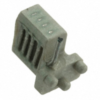
Terminal Configuration
'
No.
Terminal Name
1
Feed
2
Mechanical support studs
(
Terminal Dimensions
0.50 mm diameter Sn plated wire,
planar soldering area length 2.35 mm
1.00 mm diam, length 0.90 mm
Pulse Finland Oy
Takatie 6
90440 Kempele, Finland
Tel: +358 207 935 500
Fax: +358 207 935 501
www.pulseeng.com/antennas
© 2007. All Rights Reserved.
�W3110 Datasheet version 2.2. 1.575 GHz Helical GPS SMD Antenna. Confidential. Preliminary (06/07)
1.575 GHz Helical GPS SMD Antenna
Ground cleared under antenna, clearance area 7.50 x 5.50 mm
Recommended test board layout for electrical characteristic measurement,
test board outline size 100 x 40 mm
Feed line should be designed to match 50 Ω characteristic impedance, depending on PWB material and thickness.
+&�E^c�\[[Z�b_d[
I^kdj�_dZkYjeh�\eh�cWjY^_d]
p
')�6j\�'%%+�%-/)*/&&
')�6j\�'%%+�%-/)*/&&
8=&BVg`Zgh
8=&BVg`Zgh
p
'$'$#'-$+'(�Z8
($��#)($&*&�Z8'+-+$*(&&&&�C>p
'+-+$*(&&&&�C>p
($��#)($&*&�Z8
)$��#',$+)/�Z8'$+.+&&�=>p
'$+.+&&�=>p
)$��#',$+)/�Z8
')�6j\�'%%+�%-/))/&&
')�6j\�'%%+�%-/))/&&
9>'�I''�BE=
9>'�I''�BE=
p
($��#)($&*&�Z8
'+-+$*(&&&&�C>p
($��#)($&*&�Z8
'+-+$*(&&&&�C>p
)$��#',$+)/�Z8
'$+.+&&�=>p
)$��#',$+)/�Z8 '$+.+&&�=>p
9>' I''��'9>'
K��p
'$'$,'$*.*�²
($��+&$-()�²���#($('(/�²��
#($('(/�²��� *+$,+(�f<
� *+$,+(�f<
($��+&$-()�²���
'�+-+$*(&�&&&�C>p
'�+-+$*(&�&&&�C>p
)/$'+.�²� #,$-,/+�²�
#,$-,/+�²� '$�+.+&&�=>p
'$�+.+&&�=>p
)$)$)/$'+.�²�
K��'
9eh K��'I''��'
I''��'
K��p
IF7D�+&&$&&&�&&&�C>p
IF7D�+&&$&&&�&&&�C>p
9;DJ;H�'�+-+$*(&�&&&�C>p
9;DJ;H�'�+-+$*(&�&&&�C>p
9;DJ;H�'�+-+$*(&�&&&�C>p
9;DJ;H�'�+-+$*(&�&&&�C>p
IF7D�+&&$&&&�&&&�C>p
IF7D�+&&$&&&�&&&�C>p
IF7D�+&&$&&&�&&&�C>p
IF7D�+&&$&&&�&&&�C>p
9;DJ;H�'�+-+$*(&�&&&�C>p
9;DJ;H�'�+-+$*(&�&&&�C>p
IF7D�+&&$&&&�&&&�C>p
IF7D�+&&$&&&�&&&�C>p
Free space efficiency and maximum gain
PWB ground clearance area 7.50 x 5.50 mm
#($&&
G=8E�
很抱歉,暂时无法提供与“W3110”相匹配的价格&库存,您可以联系我们找货
免费人工找货- 国内价格 香港价格
- 800+10.78839800+1.39577
- 1600+10.490371600+1.35721
- 2400+10.341082400+1.33790
- 4000+10.175744000+1.31651
- 5600+10.079085600+1.30400
- 8000+9.986158000+1.29198
- 国内价格 香港价格
- 1+20.094051+2.59971
- 10+14.8730210+1.92423
- 25+13.5629025+1.75473
- 100+12.12516100+1.56872
- 250+11.43929250+1.47998
- 国内价格
- 800+6.40824
- 1600+6.31151
- 2400+6.21478