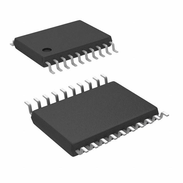
291PGLF

291PGLF

  • 厂商:

    RENESAS(瑞萨)

  • 封装:

    TSSOP-20

  • 描述:

    IC CLK SYNTH TRPL PLL 20-TSSOP

  • 详情介绍
  • 数据手册
  • 价格&库存
291PGLF 数据手册
DATASHEET TRIPLE PLL FIELD PROG. SPREAD SPECTRUM CLOCK SYNTHESIZER ICS291 Description Features The ICS291 field programmable spread spectrum clock synthesizer generates up to six high-quality, high-frequency clock outputs including multiple reference clocks from a low-frequency crystal input. It is designed to replace crystals, crystal oscillators and stand alone spread spectrum devices in most electronic systems. • • • • • • • • • Using IDT’s VersaClockTM software to configure PLLs and outputs, the ICS291 contains a One-Time Programmable (OTP) ROM for field programmability. Programming features include input/output frequencies, spread spectrum amount, eight selectable configuration registers and up to two sets of three low-skew outputs. Each of the two output groups are powered by a separate VDDO voltage. VDDO may vary from 1.8 V to VDD. Using Phase-Locked Loop (PLL) techniques, the device runs from a standard fundamental mode, inexpensive crystal, or clock. It can replace multiple crystals and oscillators, saving board space and cost. • • • • Packaged as 20-pin TSSOP – Pb-free, RoHS compliant Eight addressable registers Replaces multiple crystals and oscillators Output frequencies up to 200 MHz at 3.3 V Configurable Spread Spectrum Modulation Input crystal frequency of 5 to 27 MHz Clock input frequency of 3 to 166 MHz Up to six reference outputs Separate 1.8 to 3.3 V VDDO output level controls for each bank of 3 outputs Up to two sets of three low-skew outputs Operating voltages of 3.3 V Controllable output drive levels Advanced, low-power CMOS process The ICS291 is also available in factory programmed custom versions for high-volume applications. Block Diagram VDD S2:S0 3 OTP ROM with PLL Values VDDO1 3 PLL1 with Spread Spectrum CLK1 CLK2 Divide Logic and Output Enable Control PLL2 PLL3 CLK3 CLK4 CLK5 X1/ICLK Crystal or Clock Input Crystal Oscillator CLK6 X2 External capacitors are required with a crystal input. GND 3 PDTS IDT™ / ICS™ TRIPLE PLL FIELD PROG. SPREAD SPECTRUM CLOCK SYNTHESIZER 1 VDDO2 ICS291 REV F 051310 ICS291 TRIPLE PLL FIELD PROG. SPREAD SPECTRUM CLOCK SYNTHESIZER EPROM CLOCK SYNTHESIZER Pin Assignment 20 S2 2 19 VDD S1 VDD 3 18 PDTS 4 17 GND VDDO1 5 16 CLK6 CLK1 6 15 CLK5 CLK2 7 14 CLK4 CLK3 GND 8 13 9 12 VDDO2 VDD 10 11 X2 GND 1 S0 X1/ICLK 20 pin (173 mil) TSSOP Pin Descriptions Pin Number Pin Name Pin Type 1 GND Power Connect to ground. 2 S0 Input Select pin 0. Internal pull-up resistor. Pin Description 3 S1 Input 4 VDD Power Select pin 1. Internal pull-up resistor. Connect to +3.3 V. 5 VDDO1 Power Power supply for outputs CLK1-CLK3. 6 CLK1 Output Output clock 1. Weak internal pull-down when tri-state. 7 CLK2 Output Output clock 2. Weak internal pull-down when tri-state. 8 CLK3 Output Output clock 3. Weak internal pull-down when tri-state. 9 GND Power Connect to ground. 10 X1/ICLK XI Crystal input. Connect this pin to a crystal or external input clock. 11 X2 XO 12 VDD Power Crystal Output. Connect this pin to a crystal. Float for clock input. Connect to +3.3 V. 13 VDDO2 Power Power supply for outputs CLK4-CLK6. 14 CLK4 Output Output clock 4. Weak internal pull-down when tri-state. 15 CLK5 Output Output clock 5. Weak internal pull-down when tri-state. 16 CLK6 Output Output clock 6. Weak internal pull-down when tri-state. 17 GND Power Connect to ground. 18 PDTS Input 19 VDD Power Power-down tri-state. Powers down entire chip and tri-states clock outputs when low. Internal pull-up resistor. Connect to +3.3 V. 20 S2 Input Select pin 2. Internal pull-up resistor. IDT™ / ICS™ TRIPLE PLL FIELD PROG. SPREAD SPECTRUM CLOCK SYNTHESIZER 2 ICS291 REV F 051310 ICS291 TRIPLE PLL FIELD PROG. SPREAD SPECTRUM CLOCK SYNTHESIZER External Components EPROM CLOCK SYNTHESIZER The ICS291 requires a minimum number of external components for proper operation. The ICS291 also provides separate output divide values, from 2 through 63, to allow the two output clock banks to support widely differing frequency values from the same PLL. Series Termination Resistor Each output frequency can be represented as: Clock output traces over one inch should use series termination. To series terminate a 50Ω trace (a commonly used trace impedance), place a 33Ω resistor in series with the clock line, as close to the clock output pin as possible. The nominal impedance of the clock output is 20Ω. Decoupling Capacitors As with any high-performance mixed-signal IC, the ICS291 must be isolated from system power supply noise to perform optimally. OutputFreq = REFFreq ⋅ M ----N Output Drive Control The ICS291 has two output drive settings. For VDDO=VDD, low drive should be selected when outputs are less than 100 MHz. High drive should be selected when outputs are greater than 100 MHz. Decoupling capacitors of 0.01µF must be connected between each VDD and the PCB ground plane. For optimum device performance, the decoupling capacitor should be mounted on the component side of the PCB. Avoid the use of vias on the decoupling circuit. For VDDO
291PGLF
物料型号:ICS291

器件简介:ICS291是一款可编程展频时钟综合器,能够从低频晶体输入生成多达六个高质量、高频时钟输出,包括多个参考时钟。它旨在替代大多数电子系统中的晶体、晶体振荡器和独立展频设备。

引脚分配:ICS291采用20引脚TSSOP封装,每个引脚具有特定的功能,例如GND连接地、VDDO提供输出时钟的电源、CLKx输出时钟信号等。

参数特性:包括可编程的输入/输出频率、展频量、八个可寻址配置寄存器、多达两组三路低偏斜输出等。输出频率可高达200 MHz,输入晶体频率范围为5至27 MHz。

功能详解:ICS291使用相位锁定环(PLL)技术,可以配置为标准基频模式、廉价晶体或时钟输入。它还可以通过IDT的VersaClock™软件进行配置,以生成最低抖动、最低功耗的配置。

应用信息:ICS291适用于需要高频率、低抖动和展频特性的电子系统,如通信设备、高性能计算等。

封装信息:ICS291提供20引脚TSSOP封装,符合无铅和RoHS标准。

291PGLF 价格&库存

很抱歉,暂时无法提供与“291PGLF”相匹配的价格&库存,您可以联系我们找货

免费人工找货