6V49205BNLGI8

6V49205BNLGI8

  • 厂商:

    RENESAS(瑞萨)

  • 封装:

    VFQFN-48

  • 描述:

  • 详情介绍
  • 数据手册
  • 价格&库存
6V49205BNLGI8 数据手册
6V49205B Freescale P10XX and P20XX System Clock with Selectable DDR Frequency DATASHEET Description Typical Applications The 6V49205B is a main clock for Freescale P10xx and P20xx-based systems. It has a selectable System CCB clock and 2 DDRCLK speeds – 100M or 66.66M. The 6V49205B also provides LP-HCSL PCIe outputs for low power and reduced board space. System Clock for Freescale P10xx and P20xx-based designs Features • Replaces 11 crystals, 2 oscillators and 3 clock generators; lowers cost, power and area • Integrated terminations on LP-HCSL PCIe outputs; Output Features • 1 – Sys_CCB 3.3V LVCMOS output at 100M/83.33M/ • • • • • • • • 80M/66.66M 1 – DDRCLK 3.3V LVCMOS output at 100M or 66.66M 1 1 – 125M 3.3V LVCMOS output 6 – LP-HCSL PCIe pairs selectable at 100M or 125M 6 – 25MHz 3.3V LVCMOS outputs 2 – 2.048M 3.3V LVCMOS outputs 2 – USB 3.3V LVCMOS outputs at12M or 24M • • Key Specifications eliminate 24 resistors, saving 41mm2 of board area Industrial temperature range operation; supports demanding environmental conditions Advanced 3.3V CMOS process; high-performance, low-power Supports independent spread spectrum on Sys_CCB/DDRCLK and PCIe outputs Available in 48-pin TSSOP and space-saving 7 x 7 mm 48-pin VFQFPN with 0.5mm pad pitch; reduced board space without the need for fine-pitch assembly techniques • PCIe Gen1–2–3 compliant •
6V49205BNLGI8
物料型号:6V49205B 器件简介:6V49205B 是 Freescale P10xx 和 P20xx 系统的基础时钟,提供可选择的系统 CCB 时钟和 2 种 DDRCLK 速度 - 100M 或 66.66M。

该器件还提供 LP-HCSL PCIe 输出,用于降低功耗和减少板空间。

引脚分配:文档提供了详细的引脚分配表,包括每个引脚的名称、类型、描述等。

参数特性:包括工业温度范围操作、高性能、低功耗的 3.3V CMOS 工艺,以及支持通过 SMBus 选择的系统时钟和 DDR 时钟的展频等。

功能详解:包括 PLL1 (带 SS)、SCLK、DDRCLK、SDATA、Control Logic 等的详细功能描述。

应用信息:适用于基于 Freescale P10xx 和 P20xx 设计的系统时钟。

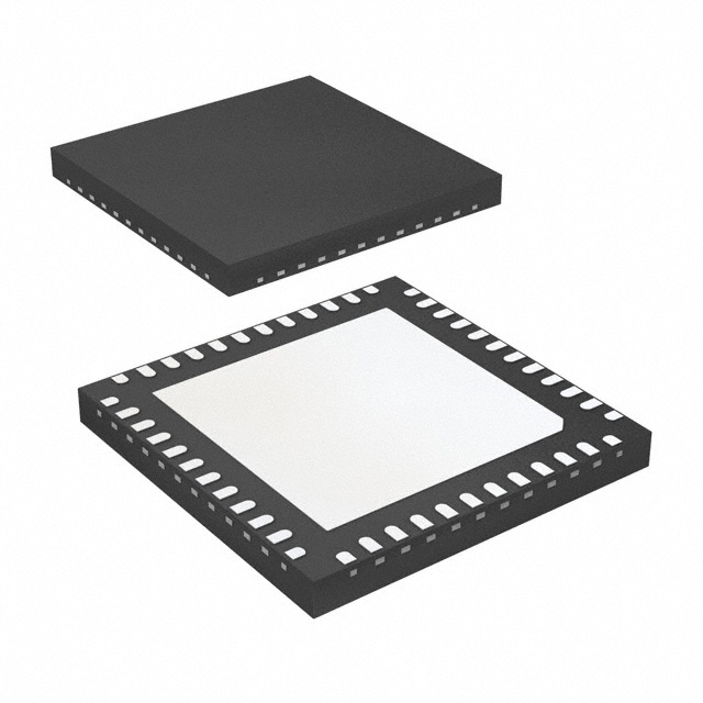
封装信息:提供 48 引脚 TSSOP 和节省空间的 7 x 7 mm 48 引脚 VFQFPN,0.5mm 焊盘间距。
6V49205BNLGI8 价格&库存

很抱歉,暂时无法提供与“6V49205BNLGI8”相匹配的价格&库存,您可以联系我们找货

免费人工找货