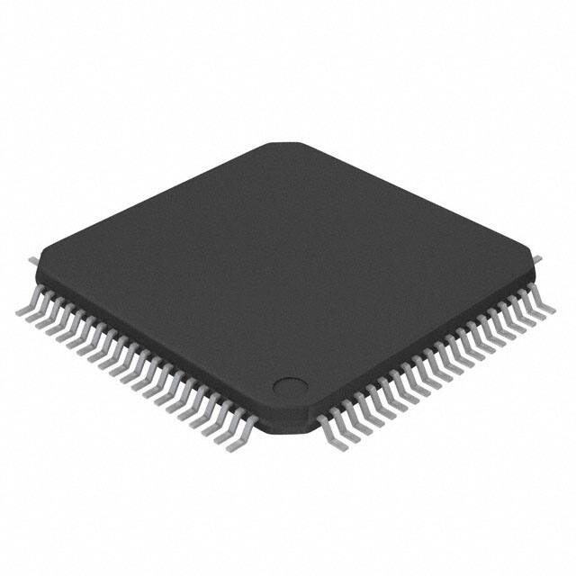
IDT70914S
HIGH SPEED 36K (4K X 9)
SYNCHRONOUS
DUAL-PORT RAM
Features
◆
◆
◆
◆
High-speed clock-to-data output times
– Military: 20/25ns (max.)
– Commercial: 12/15/20ns (max.)
Low-power operation
– IDT70914S
Active: 850 mW (typ.)
Standby: 50 mW (typ.)
Architecture based on Dual-Port RAM cells
– Allows full simultaneous access from both ports
Synchronous operation
– 4ns setup to clock, 1ns hold on all control, data, and address
inputs
– Data input, address, and control registers
◆
◆
◆
◆
◆
◆
◆
– Fast 12ns clock to data out
– Self-timed write allows fast cycle times
– 16ns cycle times, 60MHz operation
TTL-compatible, single 5V (+ 10%) power supply
Clock Enable feature
Guaranteed data output hold times
Available in 68-pin PLCC, and 80-pin TQFP
Military product compliant to MIL-PRF-38535 QML
Industrial temperature range (-40°C to +85°C) is available
for selected speeds.
Recommended for replacement of IDT7099 (4K x 9) if
separate 9th bit data control signals are not required.
Functional Block Diagram
WRITE
LOGIC
WRITE
LOGIC
MEMOR
MEMORY
Y
ARRAY
ARRAY
REGISTER
REGISTER
I/O0-8L
I/O0-8R
SENSE
SENSE
AMPS DECODER DECODER AMPS
OEL
CLKL
CLKENL
R/WL
REG
en
REG
en
REG
CEL
OER
CLKR
CLKENR
Selftimed
Write
Logic
Selftimed
Write
Logic
A0L-A11L
A0R-A11R
REG
R/WR
CER
3490 drw 01
OCTOBER 2008
1
©2008 Integrated Device Technology, Inc.
DSC-3490/7
�IDT70914S
High-Speed 36K (4K x 9) Synchronous Dual-Port Static RAM
Military, Industrial and Commercial Temperature Ranges
Description
reception error checking.
Fabricated using IDT’s CMOS high-performance technology, these
Dual-Ports typically operate on only 850mW of power at maximum highspeed clock-to-data output times as fast as 12ns. An automatic power
down feature, controlled by CE, permits the on-chip circuitry of each port
to enter a very low standby power mode.
The IDT70914 is packaged in a 68-pin PLCC, and an 80-pin TQFP.
Military grade product is manufactured in compliance with the latest revision
of MIL-PRF-38535 QML, making it ideally suited for military temperature
applications demanding the highest level of performance and reliability.
The IDT70914 is a high-speed 4K x 9 bit synchronous Dual-Port RAM.
The memory array is based on Dual-Port memory cells to allow
simultaneous access from both ports. Registers on control, data, and
address inputs provide low set-up and hold times. The timing latitude
provided by this approach allow systems to be designed with very short
cycle times. With an input data register, this device has been optimized for
applications having unidirectional data flow or bi-directional data flow in
bursts.
The IDT70914 utilizes a 9-bit wide data path to allow for parity at the
user's option. This feature is especially useful in data communication
applications where it is necessary to use a parity bit for transmission/
A5L
A4L
A3L
A2L
A1L
A0L
CLKENL
CLKL
CLKR
CLKENR
A0R
A1R
A2R
A3R
A4R
A5R
A6R
Pin Configurations(1,2,3)
INDEX
9
A6L
A7L
A8L
A9L
A10L
A11L
OEL
N/C
VCC
R/WL
N/C
N/C
CEL
GND
I/O8L
I/O7L
I/O6L
8
7
6
5
4
10
3
2
68 67 66 65 64 63 62 61
1
60
11
59
12
58
13
57
14
56
15
55
IDT70914J
J68-1(4)
16
17
18
54
53
52
68-Pin PLCC
Top View(5)
19
20
51
50
21
49
22
48
23
47
24
46
25
45
44
26
27 28 29 30 31 32 33 34 35 36 37 38 39 40 41 42 43
A7R
A8R
A9R
A10R
A11R
OER
N/C
GND
GND
R/WR
N/C
N/C
CER
GND
I/O8R
I/O7R
I/O6R
N/C
I/O5L
VCC
I/O4L
I/O3L
I/O2L
I/O1L
I/O0L
GND
GND
I/O0R
I/O1R
I/O2R
I/O3R
VCC
I/O4R
I/O5R
,
NOTES:
1. All VCC pins must be connected to power supply.
2. All ground pins must be connected to ground supply.
3. J68-1 package body is approximately .95 in x .95 in x .17 in.
4. This package code is used to reference the package diagram.
5. This text does not indicate orientation of the actual part-marking.
6.42
2
3490 drw 03
�IDT70914S
High-Speed 36K (4K x 9) Synchronous Dual-Port Static RAM
Military, Industrial and Commercial Temperature Ranges
N/C
N/C
A5L
A4L
A3L
A2L
A1L
A0L
CLKENL
CLKL
CLKR
CLKENR
A0R
A1R
A2R
A3R
A4R
A5R
A6R
N/C
Pin Configuration(1,2,3) (con't.)
Reference
N/C
A6L
A7L
A8L
A9L
A10L
A11L
N/C
OEL
N/C
VCC
R/WL
N/C
N/C
CEL
GND
I/O8L
I/O7L
I/O6L
N/C
1
2
80 79 78 77 76 75 74 73 72 71 70 69 68 67 66 65 64 63 62 61
60
59
3
58
4
57
5
56
6
55
7
IDT70914PF
PN80-1(4)
8
9
10
54
53
52
51
80-Pin TQFP
Top View(5)
11
12
50
49
13
48
14
47
15
46
16
45
17
44
18
43
19
42
20
41
N/C
N/C
I/O5L
VCC
I/O4L
I/O3L
I/O2L
I/O1L
I/O0L
GND
GND
I/O0R
I/O1R
I/O2R
I/O3R
VCC
I/O4R
I/O5R
N/C
N/C
21 22 23 24 25 26 27 28 29 30 31 32 33 34 35 36 37 38 39 40
NOTES:
1. All VCC pins must be connected to power supply.
2. All ground pins must be connected to ground supply.
3. PN80-1 package body is approximately 14mm x 14mm x 1.4mm.
4. This package code is used to reference the package diagram.
5. This text does not indicate orientation of the actual part-marking.
6.42
3
N/C
A7R
A8R
A9R
A10R
A11R
N/C
OER
N/C
GND
GND
R/WR
N/C
N/C
CER
GND
I/O8R
I/O7R
I/O6R
N/C
,
3490 drw 04
�IDT70914S
High-Speed 36K (4K x 9) Synchronous Dual-Port Static RAM
Absolute Maximum Ratings(1)
Symbol
Commercial
& Industrial
Military
Terminal Voltage
with Respect
to GND
-0.5 to +7.0
-0.5 to +7.0
VTERM(2)
Terminal Voltage
-0.5 to VCC
-0.5 to VCC
V
TBIAS
Temperature
Under Bias
-55 to +125
-65 to +135
o
-65 to +150
-65 to +150
o
50
50
VTERM(2)
Rating
TSTG
Storage
Temperature
IOUT
DC Output
Current
Military, Industrial and Commercial Temperature Ranges
Maximum Operating Temperature
and Supply Voltage(1,2)
Unit
Grade
V
Military
Commercial
Industrial
C
Ambient
Temperature
GND
VCC
-55OC to+125OC
0V
5.0V + 10%
0OC to +70OC
0V
5.0V + 10%
-40OC to +85OC
0V
5.0V + 10%
3490 tbl 02
NOTES:
1. This is the parameter TA. This is the "instant on" casae temperature.
2. Industrial temperature: for specific speeds, packages and powers contact your
C
mA
3490 tbl 01
NOTES:
1. Stresses greater than those listed under ABSOLUTE MAXIMUM RATINGS may
cause permanent damage to the device. This is a stress rating only and functional
operation of the device at these or any other conditions above those indicated
in the operational sections of this specification is not implied. Exposure to absolute
maximum rating conditions for extended periods may affect reliability.
2. VTERM must not exceed VCC + 10% for more than 25% of the cycle time or 10ns
maximum, and is limited to < 20mA for the period of VTERM > Vcc + 10%.
Recommended DC Operating
Conditions
Symbol
CIN
COUT
Supply Voltage
GND
Ground
V IL
(TA = +25°C, f = 1.0MHz) TQFP Only
Symbol
VCC
VIH
Capacitance
Parameter
Conditions
Max.
Unit
VIN = 3dV
8
pF
VOUT = 3dV
9
pF
Input Capacitance
Output Capacitance
Parameter
Input High Voltage
Input Low Voltage
Min.
Typ.
Max.
Unit
4.5
5.0
5.5
V
0
0
0
V
2.2
____
-0.5
(1)
(2)
6.0
____
0.8
V
V
3490 tbl 03
NOTES:
1. VIL > -1.5V for pulse width less than 10ns.
2. VTERM must not exceed VCC + 10%.
3490 tbl 04
NOTES:
1. These parameters are determined by device characterization, but are not
production tested.
2. 3dV references the interpolated capacitance when the input and output switch
from 0V to 3V or from 3V to 0V.
DC Electrical Characteristics Over the Operating
Temperature and Supply Voltage Range (VCC = 5.0V ± 10%)
70914S
Symbol
Parameter
Test Conditions
Min.
Max.
Unit
Input Leakage Current(1)
VCC = 5.5V, VIN = 0V to V CC
___
10
µA
|ILO|
Output Leakage Current
CE = VIH, VOUT = 0V to V CC
___
10
µA
VOL
Output Low Voltage
IOL = +4mA
___
0.4
V
VOH
Output High Voltage
IOH = -4mA
2.4
___
|ILI|
V
3490 tbl 05
NOTE:
1. At VCC < 2.0V, input leakages are undefined
6.42
4
�IDT70914S
High-Speed 36K (4K x 9) Synchronous Dual-Port Static RAM
Military, Industrial and Commercial Temperature Ranges
DC Electrical Characteristics Over the Operating
Temperature and Supply Voltage Range(4,5) (VCC = 5V ± 10%)
70914S12
Com'l Only
Symbol
ICC
ISB1
ISB2
ISB3
ISB4
Parameter
Test Condition
Version
70914S15
Com'l Only
Typ.(2)
Max.
Typ.(2)
Max.
Unit
mA
Dynamic Operating
Current
(Both Ports Active)
CEL and CER = VIL,
Outputs Disabled
f = fMAX(1)
COM'L
190
310
180
300
MIL &
IND
____
____
____
____
Standby Current
(Both Ports - TTL
Level Inputs)
CEL and CER = VIH
f = fMAX(1)
COM'L
95
150
90
140
MIL &
IND
____
____
____
____
Standby Current
(One Port - TTL
Level Inputs)
CE"A" = VIL and
CE"B" = VIH(3)
Active Port Outputs
Disabled, f=fMAX(1)
COM'L
170
220
160
210
MIL &
IND
____
____
____
____
Full Standby
Current (Both
Ports - All CMOS
Level Inputs)
Both Ports CER and
CEL > VCC - 0.2V
VIN > VCC - 0.2V or
VIN < 0.2V, f = 0(2)
COM'L
10
15
10
15
MIL &
IND
____
____
____
____
Full Standby
Current (One
Port - All CMOS
Level Inputs)
CE"A" < 0.2V and
CE"B" > VCC - 0.2V(3)
VIN > VCC - 0.2V or
VIN < 0.2V, Active Port
Outputs Disabled
f = fMAX(1)
COM'L
165
210
155
200
MIL &
IND
____
____
____
____
mA
mA
mA
mA
3490 tbl 06a
70914S20
Com'l &
Military
Symbol
ICC
ISB1
ISB2
ISB3
ISB4
Parameter
Test Condition
Version
70914S25
Military
Only
Typ.(2)
Max.
Typ.(2)
Max.
Unit
mA
Dynamic Operating
Current
(Both Ports Active)
CEL and CER = VIL,
Outputs Disabled
f = fMAX(1)
COM'L
170
290
____
____
MIL &
IND
170
310
160
290
Standby Current
(Both Ports - TTL
Level Inputs)
CEL and CER = VIH
f = fMAX(1)
COM'L
85
130
____
____
MIL &
IND
85
140
80
130
Standby Current
(One Port - TTL
Level Inputs)
CE"A" = VIL and
CE"B" = VIH(3)
Active Port Outputs
Disabled, f=fMAX(1)
COM'L
150
200
____
____
MIL &
IND
150
210
140
200
Full Standby
Current (Both
Ports - All CMOS
Level Inputs)
Both Ports CER and
CEL > VCC - 0.2V
VIN > VCC - 0.2V or
VIN < 0.2V, f = 0(2)
COM'L
10
15
____
____
MIL &
IND
10
20
10
20
Full Standby
Current (One
Port - All CMOS
Level Inputs)
CE"A" < 0.2V and
CE"B" > VCC - 0.2V(3)
VIN > VCC - 0.2V or
VIN < 0.2V, Active Port
Outputs Disabled
f = fMAX(1)
COM'L
145
190
____
____
MIL &
IND
145
200
135
190
mA
mA
mA
mA
3490 tbl 06b
NOTES:
1. At f MAX, address and control lines (except Output Enable) are cycling at the maximum frequency clock cycle of 1/t CYC, using "AC TEST CONDITIONS" at input levels
of GND to 3V.
2. f = 0 means no address, clock, or control lines change. Applies only to input at CMOS level standby.
3. Port "A" may be either left or right port. Port "B" is the opposite from port "A".
4. Vcc = 5V, T A = 25°C for Typ, and are not production tested. ICC DC = 150mA (Typ).
5. Industrial temperature: for specific speeds, packages and powers contact your sales office.
6.42
5
�IDT70914S
High-Speed 36K (4K x 9) Synchronous Dual-Port Static RAM
Military, Industrial and Commercial Temperature Ranges
AC Test Conditions
Input Pulse Levels
GND to 3.0V
Input Rise/Fall Times
3ns Max.
Input Timing Reference Levels
1.5V
Output Reference Levels
1.5V
Output Load
Figures 1,2 and 3
3490 tbl 07
5V
5V
893Ω
893Ω
DATAOUT
DATAOUT
30pF
347Ω
3490 drw 05
3490 drw 06
Figure 1. AC Output Test load.
8
7
5pF*
347Ω
Figure 2. Output Test Load
(For tCKLZ, tCKHZ, tOLZ, and t OHZ).
*Including scope and jig.
- 9pF is the I/O capacitance
of this device, and 30pF is the
AC Test Load Capacitance
6
∆tCD
(Typical, ns)
5
4
3
2
1
0
-1
20 40 60 80 100 120 140 160 180 200
Capacitance (pF)
3490 drw 07
Figure 3. Typical Output Derating (Lumped Capacitive Load).
6.42
6
,
,
�IDT70914S
High-Speed 36K (4K x 9) Synchronous Dual-Port Static RAM
Military, Industrial and Commercial Temperature Ranges
AC Electrical Characteristics Over the Operating Temperature Range
(Read and Write Cycle Timing)(3)
(Commercial: VCC = 5V ± 10%, TA = 0°C to +70°C; Military: VCC = 5V ± 10%, TA = -55°C to +125°C)
70914S12
Com'l Only
Symbol
Parameter
70914S15
Com'l Only
Min.
Max.
Min.
Max.
Unit
20
____
ns
6
____
ns
____
ns
tCYC
Clock Cycle Time
16
____
tCH
Clock High Time
6
____
6
____
6
____
tCL
Clock Low Time
tCD
Clock High to Output Valid
12
____
15
ns
tS
Registered Signal Set-up Time
4
____
4
____
ns
tH
Registered Signal Hold Time
1
____
1
____
ns
tDC
Data Output Hold After Clock High
3
____
3
____
ns
2
____
2
____
ns
tCKLZ
(1,2)
Clock High to Output Low-Z
(1,2)
tCKHZ
Clock High to Output High-Z
____
7
____
7
ns
tOE
Output Enable to Output Valid
____
7
____
8
ns
ns
(1,2)
tOLZ
Output Enable to Output Low-Z
0
____
0
____
tOHZ
Output Disable to Output High-Z(1,2)
____
7
____
7
ns
tSCK
Clock Enable, Disable Set-up Time
4
____
4
____
ns
tHCK
Clock Enable, Disable Hold Time
2
____
2
____
ns
ns
Port-to-Port Delay
tCWDD
Write Port Clock Hig h to Read Data Delay
____
25
____
30
tCSS
Clock-to-Clock Setup Time
____
13
____
15
ns
3490 tbl 08a
70914S20
Com'l &
Military
Symbol
Parameter
70914S25
Military
Only
Min.
Max.
Min.
Max.
Unit
25
____
ns
10
____
ns
ns
tCYC
Clock Cycle Time
20
____
tCH
Clock High Time
8
____
8
____
10
____
____
20
____
25
ns
5
____
6
____
ns
1
____
ns
3
____
ns
ns
ns
tCL
Clock Low Time
tCD
Clock High to Output Valid
tS
Registered Signal Set-up Time
tH
Registered Signal Hold Time
1
____
tDC
Data Output Hold After Clock High
3
____
(1,2)
tCKLZ
Clock High to Output Low-Z
2
____
2
____
tCKHZ
Clock High to Output High-Z(1,2)
____
9
____
12
____
10
____
12
ns
0
____
0
____
ns
____
9
____
11
ns
ns
tOE
Output Enable to Output Valid
tOLZ
Output Enable to Output Low-Z(1,2)
tOHZ
Output Disable to Output High-Z(1,2)
tSCK
Clock Enable, Disable Set-up Time
5
____
6
____
tHCK
Clock Enable, Disable Hold Time
2
____
2
____
ns
Write Port Clock Hig h to Read Data Delay
____
35
____
45
ns
Clock-to-Clock Setup Time
____
15
____
20
Port-to-Port Delay
tCWDD
tCSS
NOTES:
1. Transition is measured 0mV from Low or High impedance voltage with the Output Test Load (Figure 2).
2. This parameter is guaranteed by device characterization, but is not production tested.
3. Industrial temperature: for specific speeds, packages and powers contact your sales office.
6.42
7
ns
3490 tbl 08b
�IDT70914S
High-Speed 36K (4K x 9) Synchronous Dual-Port Static RAM
Military, Industrial and Commercial Temperature Ranges
Timing Waveform of Read Cycle, Either Side
tCYC
tCH
CLK
tCL
tSCK
tSCK
tHCK
CLKEN
tS
tH
CE
R/W
ADDRESS
An
An + 1
An + 2
An + 3
tCKHZ (1)
tDC
tCD
DATAOUT
Qn
Qn + 1
tCKLZ (1)
tOHZ
Qn + 1
(1)
tOLZ
(1)
tOE
OE
3490 drw 08
Timing Waveform of Write with Port-to-Port Read(2,3,4)
CLK "A"
R/W "A"
ADDR "A"
DATA IN "A"
NO
MATCH
MATCH
VALID
tCCS
(5)
CLK "B"
tCD
R/W "B"
ADDR "B"
NO
MATCH
MATCH
tCWDD
tCD
DATA OUT "B"
VALID
VALID
tDC
3490 drw 09
NOTES:
1. Transition is measured ±200mV from Low or High-impedance voltage with the Output Test Load (Figure 2).
2. CE L = CER = VIL, CLKENL = CLKENR = VIL.
3. OE = V IL for the reading port, port 'B'.
4. All timing is the same for left and right ports. Ports "A" may be either the left or right port. Port "B" is opposite from port "A".
5. If t CCS < maximum specified, then data from right port READ is not valid until the maximum specified for tCWDD.
If t CCS > maximum specified, then data from right port READ is not valid until tCCS + tCD. tCWDD does not apply in this case.
6.42
8
�IDT70914S
High-Speed 36K (4K x 9) Synchronous Dual-Port Static RAM
Military, Industrial and Commercial Temperature Ranges
Timing Waveform of Read-to-Write Cycle No. 1(1,2) (tCYC = min.)
tCYC
tCH
CLK
tCYC
tCL
tCH
tCL
CLKEN
tS
tH
(1)
CE
R/W
ADDRESS
An
An + 1
An + 1
(1)
An + 2
(1)
Dn + 1
DATAIN
Dn + 2
tCKHZ (3)
tCD
DATAOUT
Qn
tCKLZ (3)
3490 drw 10
Timing Waveform of Read-to-Write Cycle No. 2(4) (tCYC > min.)
tCYC
(4)
tCH
CLK
tCL
CLKEN
tS
tH
CE
R/W
ADDRESS
An
An + 1
DATAIN
Dn + 1
tCD
DATAOUT
tCKLZ
Qn
(3)
tOHZ
OE
3490 drw 11
NOTES:
1. For tCYC = min.; data out coincident with the rising edge of the subsequent write clock can occur. To ensure writing to the correct address location, the write must
be repeated on the second write clock rising edge. If CE = VIL, invalid data will be written into array. The An+1 must be rewritten on the following cycle.
2. OE LOW throughout.
3. Transition is measured 0mV from Low or High-impedance voltage with the Output Test Load (Figure 2).
4. For t CYC > min.; OE may be used to avoid data out coincident with the rising edge of the subsequent write clock. Use of OE will eliminate the need for the write to
be repeated.
6.42
9
�IDT70914S
High-Speed 36K (4K x 9) Synchronous Dual-Port Static RAM
Military, Industrial and Commercial Temperature Ranges
Functional Description
The IDT70914 provides a true synchronous Dual-Port Static RAM
interface. Registered inputs provide very short set-up and hold times on
address, data, and all critical control inputs. All internal registers are clocked
on the rising edge of the clock signal. An asynchronous output enable is
provided to ease asynchronous bus interfacing.
The internal write pulse width is dependent on the LOW to HIGH
transitions of the clock signal allowing the shortest possible realized cycle
times. Clock enable inputs are provided to stall the operation of the address
and data input registers without introducing clock skew for very fast
interleaved memory applications.
A HIGH on the CE input for one clock cycle will power down the
internal circuitry to reduce static power consumption.
Truth Table I: Read/Write Control(1)
Inputs
(3)
Synchronous
Outputs
Asynchronous
Mode
CLK
CE
R/W
OE
I/O0-8
↑
H
X
X
High-Z
Deselected, Power-Down
↑
L
L
X
DATAIN
Selected and Write Enabled
↑
L
H
L
DATAOUT
↑
X
X
H
High-Z
Read Selected and Data Output Enable Read
Outputs Disabled
3490 tbl 09
Truth Table II: Clock Enable Function Table(1)
Inputs
Register Outputs(4)
Register Inputs
Mode
CLK(3)
CLKEN(2)
ADDR
DATAIN
ADDR
DATAOUT
Load "1"
↑
L
H
H
H
H
Load "0"
↑
L
L
L
L
L
Hold (do nothing)
↑
H
X
X
NC
NC
X
H
X
X
NC
NC
3490 tbl 10
NOTES:
1. 'H' = HIGH voltage level steady state, 'h' = HIGH voltage level one set-up time prior to the LOW-to-HIGH clock transition, 'L' = LOW voltage level steady state 'l' = LOW
voltage level one set-up time prior to the LOW-to-HIGH clock transition, 'X' = Don't care, 'NC' = No change
2. CLKEN = VIL must be clocked in during Power-Up.
3. Control signals are initialted and terminated on the rising edge of the CLK, depending on their input level. When R/W and CE are LOW, a write cycle is initiated on
the LOW-to-HIGH transition of the CLK. Termination of a write cycle is done on the next LOW-to-HIGH transistion of the CLK.
4. The register outputs are internal signals from the register inputs being clocked in or disabled by CLKEN.
6.42
10
�IDT70914S
High-Speed 36K (4K x 9) Synchronous Dual-Port Static RAM
Military, Industrial and Commercial Temperature Ranges
Ordering Information
XXXX
Device
Type
A
Power
999
Speed
A
Package
A
Process/
Temperature
Range
Blank
I (1)
B
Commercial (0°C to +70°C)
Industrial (-40°C to +85°C)
Military (-55°C to +85°C)
Compliant to MIL-PRF-38535 QML
J
PF
68-pin PLCC (J68-1)
80-pin TQFP (PN80-1)
12
15
20
25
Commercial Only
Commercial Only
Commercial & Military
Military Only
S
Standard Power
70914
36K (4K x 9-Bit) Synchronous Dual-Port RAM
⎫
⎬ Speed in nanoseconds
⎭
3490 drw 12
NOTE:
1. Industrial temperature range is available on selected TQFP packages in standard power.
For specific speeds, packages and powers contact your sales office.
Datasheet Document History
3/10/99:
6/7/99:
11/10/99:
5/24/00:
1/12/01:
10/21/08:
Initiated datasheet document history
Converted to new format
Cosmetic and typographical corrections
Page 2 and 3 Added additional notes to pin configurations
Changed drawing format
Replaced IDT logo
Page 4 Increased storage temperature parameter
Clarified TA parameter
Page 5 DC Electrical parameters–changed wording from "open" to "disabled"
Changed ±200mV to 0mV in notes
Removed PGA pinout (obsolete package)
Changed cycle time of 12ns part from 17ns (58MHz) to 16ns (60MHz)
Page 11 Removed "IDT" from orderable part number
CORPORATE HEADQUARTERS
6024 Silver Creek Valley Road
San Jose, CA 95138
for SALES:
800-345-7015 or 408-284-8200
fax: 408-284-2775
www.idt.com
The IDT logo is a registered trademark of Integrated Device Technology, Inc.
6.42
11
for Tech Support:
408-284-2794
DualPortHelp@idt.com
�