CMOS SyncFIFO™
512 x 36
1,024 x 36
2,048 x 36
FEATURES:
•
•
•
•
•
•
•
•
•
•
•
Storage capacity:
IDT723631 - 512 x 36
IDT723641 - 1,024 x 36
IDT723651 - 2,048 x 36
Supports clock frequencies up to 67 MHz
Fast access times of 11ns
Free-running CLKA and CLKB can be asynchronous or coincident (permits simultaneous reading and writing of data on a
single clock edge)
Clocked FIFO buffering data from Port A to Port B
Synchronous read retransmit capability
Mailbox register in each direction
Programmable Almost-Full and Almost-Empty flags
Microprocessor interface control logic
Input Ready (IR) and Almost-Full (AF) flags synchronized by
CLKA
•
•
IDT723631
IDT723641
IDT723651
Output Ready (OR) and Almost-Empty (AE) flags synchronized
by CLKB
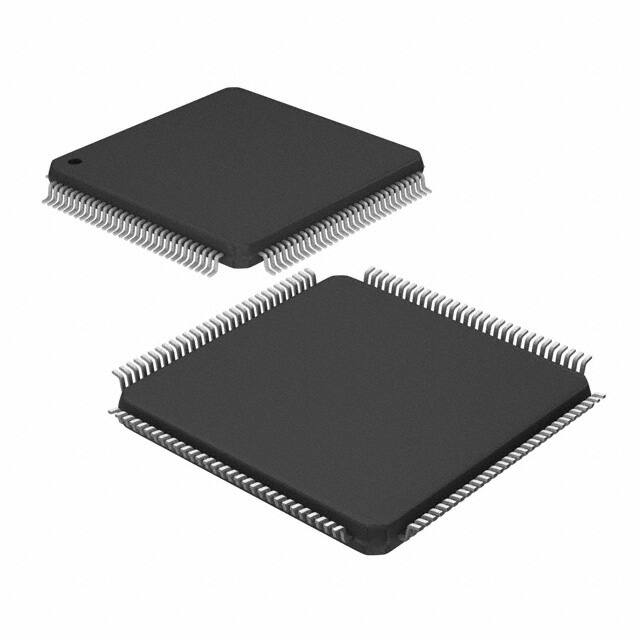
Available in space-saving 120-pin thin quad flat package (TQFP)
Green parts available, see ordering information
DESCRIPTION:
The IDT723631/723641/723651 is a monolithic high-speed, low-power,
CMOS clocked FIFO memory. It supports clock frequencies up to 67 MHz
and has read access times as fast as 11ns. The 512/1,024/2,048 x 36
dual-port SRAM FIFO buffers data from port A to Port B. The FIFO memory
has retransmit capability, which allows previously read data to be accessed again. The FIFO has flags to indicate empty and full conditions and
two programmable flags (Almost-Full and Almost-Empty) to indicate when a
selected number of words is stored in memory. Communication between
each port may take place with two 36-bit mailbox registers. Each mailbox
register has a flag to signal when new mail has been stored. Two or more
FUNCTIONAL BLOCK DIAGRAM
MBF1
RAM ARRAY
512 x 36
1,024 x 36
2,048 x 36
Reset
Logic
36
Write
Pointer
A0 - A35
Read
Pointer
IR
AF
Status Flag
Logic
FS0/SD
FS1/SEN
Flag Offset
Registers
10
Sync
Retransmit
Logic
RST
Input
Register
Port-A
Control
Logic
Output
Register
Mail 1
Register
CLKA
CSA
W/RA
ENA
MBA
Mail 2
Register
RTM
RFM
B0 - B35
OR
AE
Port-B
Control
Logic
CLKB
CSB
W/RB
ENB
MBB
3023 drw01
MBF2
IDT and the IDT logo are registered trademarks of Integrated Device Technology, Inc. The SyncFIFO is a trademark of Integrated Device Technology, Inc.
COMMERCIAL AND INDUSTRIAL TEMPERATURE RANGES
1
©2014 Integrated Device Technology, Inc. All rights reserved. Product specifications subject to change without notice.
MARCH 2014
DSC-2023/8
�IDT723631/723641/723651 CMOS SyncFIFO™
512 x 36, 1,024 x 36 and 2,048 x 36
COMMERCIAL AND INDUSTRIAL
TEMPERATURE RANGES
DESCRIPTION (CONTINUED)
port are arranged to provide a simple interface between microprocessors
and/or buses with synchronous control.
The Input Ready (IR) flag and Almost-Full (AF) flag of the FIFO are
two-stage synchronized to CLKA. The Output Ready (OR) flag and Almost-Empty (AE) flag of the FIFO are two-stage synchronized to CLKB.
Offset values for the Almost-Full and Almost-Empty flags of the FIFO can be
programmed from port A or through a serial input.
devices may be used in parallel to create wider data paths. Expansion is
also possible in word depth.
These devices are a clocked FIFO, which means each port employs a
synchronous interface. All data transfers through a port are gated to the
LOW-to-HIGH transition of a continuous (free-running) port clock by enable signals. The continuous clocks for each port are independent of one
another and can be asynchronous or coincident. The enables for each
120
119
118
117
116
115
114
113
112
111
110
109
108
107
106
105
104
103
102
101
100
99
98
97
96
95
94
93
92
91
GND
CLKA
ENA
W/RA
CSA
IR
OR
VCC
AF
AE
VCC
MBF2
MBA
RST
GND
FS0/SD
FS1/SEN
RTM
RFM
VCC
NC
MBB
GND
MBF1
GND
CSB
W/RB
ENB
CLKB
VCC
PIN CONFIGURATION
1
2
3
4
5
6
7
8
9
10
11
12
13
14
15
16
17
18
19
20
21
22
23
24
25
26
27
28
29
30
90
89
88
87
86
85
84
83
82
81
80
79
78
77
76
75
74
73
72
71
70
69
68
67
66
65
64
63
62
61
B35
B34
B33
B32
GND
B31
B30
B29
B28
B27
B26
VCC
B25
B24
GND
B23
B22
B21
B20
B19
B18
GND
B17
B16
VCC
B15
B14
B13
B12
GND
GND
A11
A10
A9
A8
A7
A6
GND
A5
A4
A3
VCC
A2
A1
A0
GND
B0
B1
B2
B3
B4
B5
GND
B6
VCC
B7
B8
B9
B10
B11
31
32
33
34
35
36
37
38
39
40
41
42
43
44
45
46
47
48
49
50
51
52
53
54
55
56
57
58
59
60
A35
A34
A33
A32
VCC
A31
A30
GND
A29
A28
A27
A26
A25
A24
A23
GND
A22
VCC
A21
A20
A19
A18
GND
A17
A16
A15
A14
A13
VCC
A12
3023 drw03
TQFP (PNG120, ORDER CODE: PF)
TOP VIEW
NOTE:
1. NC – No Connection
2
�IDT723631/723641/723651 CMOS SyncFIFO™
512 x 36, 1,024 x 36 and 2,048 x 36
COMMERCIAL AND INDUSTRIAL
TEMPERATURE RANGES
PIN DESCRIPTION
Symbol
Name
I/O
A0-A35
Port-A Data
I/O
36-bit bidirectional data port for side A.
Description
AE
Almost-Empty
Flag
O
Programmable flag synchronized to CLKB. It is LOW when the number of words in the FIFO is less than or equal to the value in
the Almost-Empty register (X).
AF
Almost-Full
Flag
O
Programmable flag synchronized to CLKA. It is LOW when the number of empty locations in FIFO is less than or equal to the
value in the Almost-Full Offset register (Y).
B0-B35
CLKA
Port-B Data
Port-A Clock
I/O
I
CLKB
Port-B Clock
I
36-bit bidirectional data port for side B.
CLKA is a continuous clock that synchronizes all data transfers through port-A and may be asynchronous or coincident to CLKB.
IR and AF are synchronous to the LOW-to-HIGH transition of CLKA.
CLKB is a continuous clock that synchronizes all data transfers through port-B and may be asynchronous or coincident to CLKA.
OR and AE are synchronous to the LOW-to-HIGH transition of CLKB.
CSA
Port-A Chip
Select
I
CSA must be LOW to enable a LOW-to-HIGH transition of CLKA to read or write data on port-A. The A0-A35 outputs are in the
high-impedance state when CSA is HIGH.
CSB
Port-B Chip
Select
I
CSB must be LOW to enable a LOW-to-HIGH transition of CLKB to read or write data on port-B. The B0-B35 outputs are in the
high-impedance state when CSB is HIGH.
ENA
Port-A Enable
I
ENA must be HIGH to enable a LOW-to-HIGH transition of CLKA to read or write data on port-A.
ENB
Port-B Enable
I
ENB must be HIGH to enable a LOW-to-HIGH transition of CLKB to read or write data on port-B.
FS1/
SEN,
Flag-Offset
Select 1/
Serial Enable
I
FS1/SEN and FS0/SD are dual-purpose inputs used for flag Offset register programming. During a device reset, FS1/SEN and
FS0/SD selects the flag offset programming method. Three Offset register programming methods are available: automatically
load one of two preset values, parallel load from port A, and serial load.
FS0/SD
Flag Offset 0/
Serial Data
IR
Input Ready
Flag
O
IR is synchronized to the LOW-to-HIGH transition of CLKA. When IR is LOW, the FIFO is full and writes to its array are
disabled. When the FIFO is in retransmit mode, IR indicates when the memory has been filled to the point of the retransmit
data and prevents further writes. IR is set LOW during reset and is set HIGH after reset.
MBA
Port-A Mailbox
Select
I
A HIGH level chooses a mailbox register for a port-A read or write operation.
MBB
Port-B Mailbox
Select
I
A HIGH level chooses a mailbox register for a port-B read or write operation. When the B0-B35 outputs are active, a HIGH
level on MBB selects data from the mail1 register for output and a LOW level selects FIFO data for output.
MBF1
Mail1 Register
Flag
O
MBF1 is set LOW by the LOW-to-HIGH transition of CLKA that writes data to the mail1 register. MBF1 is set HIGH by a
LOW-to-HIGH transition of CLKB when a port-B readis selected and MBB is HIGH. MBF1 is set HIGH by a reset.
MBF2
Mail2 Register
Flag
O
MBF2 is set LOW by the LOW-to-HIGH transition of CLKB that writes data to the mail2 register. MBF2 is set HIGH by a
LOW-to-HIGH transition of CLKA when a port-A read is selected and MBA is HIGH. MBF2 is set HIGH by a reset.
OR
Output Ready
Flag
O
OR is synchronized to the LOW-to-HIGH transition of CLKB. When OR is LOW, the FIFO is empty and reads are disabled.
Ready data is present in the output register of the FIFO when OR is HIGH. OR is forced LOW during the reset and goes
HIGH on the third LOW-to-HIGH transition of CLKB after a word is loaded to empty memory.
RFM
Read From
Mark
I
When the FIFO is in retransmit mode, a HIGH on RFM enables a LOW-to-HIGH transition of CLKB to reset the read pointer
to the beginning retransmit location and output the first selected retransmit data.
RST
Reset
I
To reset the device, four LOW-to-HIGH transitions of CLKA and four LOW-to-HIGH transitions of CLKB must occur while RST
is LOW. The LOW-to-HIGH transition of RST latches the status of FS0 and FS1 for AF and AE offset selection.
RTM
Retransmit
Mode
I
When RTM is HIGH and valid data is present in the FIFO output register (OR is HIGH), a LOW-to-HIGH transition of CLKB
selects the data for the beginning of a retransmit and puts the FIFO in retransmit mode. The selected word remains the initial
retransmit point until a LOW- to-HIGH transition of CLKB occurs while RTM is LOW, taking the FIFO out of retransmit mode.
W/RA
Port-A Write/
Read Select
I
A HIGH selects a write operation and a LOW selects a read operation on port A for a LOW-to-HIGH transition of CLKA. The
A0-A35 outputs are in the high-impedance state when W/RA is HIGH.
W/RB
Port-B Write/
Read Select
I
A LOW selects a write operation and a HIGH selects a read operation on port B for a LOW-to-HIGH transition of CLKB. The
B0-B35 outputs are in the high-impedance state when W/RB is LOW.
When serial load is selected for flag Offset register programming, FS1/SEN is used as an enable synchronous to the LOW-toHIGH transition of CLKA. When FS1/SEN is LOW, a rising edge on CLKA load the bit present on FS0/SD into the X and Y
registers. The number of bit writes required to program the Offset registers is 18/20/22. The first bit write stores the Y-register
MSB and the last bit write stores the X-register LSB.
3
�IDT723631/723641/723651 CMOS SyncFIFO™
512 x 36, 1,024 x 36 and 2,048 x 36
COMMERCIAL AND INDUSTRIAL
TEMPERATURE RANGES
ABSOLUTE MAXIMUM RATINGS OVER OPERATING FREE-AIR TEMPERATURE
RANGE (UNLESS OTHERWISE NOTED)(2)
Symbol
Rating
Commercial
Unit
–0.5 to 7
V
VCC
Supply Voltage Range
VI
Input Voltage Range
–0.5 to VCC+0.5
V
Output Voltage Range
–0.5 to VCC+0.5
V
(2)
VO
(2)
IIK
Input Clamp Current, (VI < 0 or VI > VCC)
±20
mA
IOK
Output Clamp Current, (VO = < 0 or VO > VCC)
±50
mA
IOUT
Continuous Output Current, (VO = 0 to VCC)
±50
mA
ICC
Continuous Current Through VCC or GND
±400
mA
TSTG
Storage Temperature Range
–65 to 150
°C
NOTES:
1. Stresses beyond those listed under "Absolute Maximum Ratings" may cause permanent damage to the device. These are stress ratings only and functional operation of the
device at these or any other conditions beyond those indicated under "Recommended Operating Conditions" is not implied. Exposure to absolute-maximum-rated conditions
for extended periods may affect device reliability.
2. The input and output voltage ratings may be exceeded provided the input and output current ratings are observed.
RECOMMENDED OPERATING CONDITIONS
Symbol
Parameter
Min.
Max.
Unit
4.5
5.5
V
2
—
V
VCC
Supply Voltage
VIH
HIGH Level Input Voltage
VIL
LOW-Level Input Voltage
—
0.8
V
IOH
HIGH-Level Output Current
—
–4
mA
IOL
LOW-Level Output Current
—
8
mA
TA
Operating Free-air Temperature
0
70
°C
ELECTRICAL CHARACTERISTICS OVER RECOMMENDED OPERATING
FREE-AIR TEMPERATURE RANGE (UNLESS OTHERWISE NOTED)
IDT723631
IDT723641
IDT723651
Commercial
tA = 15 ns
Parameter
Test Conditions
Min.
Typ.(1)
Max.
Unit
VOH
VCC = 4.5V,
IOH = –4 mA
2.4
—
—
V
VOL
VCC = 4.5V,
IOL = 8 mA
—
—
0.5
V
ILI
VCC = 5.5V,
VI = VCC or 0
—
—
±5
μA
ILO
VCC = 5.5V,
VO = VCC or 0
—
—
±5
μA
ICC
VCC = 5.5V,
VI = VCC –0.2V or 0
—
—
400
μA
VCC = 5.5V,
One Input at 3.4V,
mA
ΔICC(2,3)
Other Inputs at VCC or GND
CSA = VIH
A0-A35
—
0
—
CSB = VIH
B0-B35
—
0
—
CSA = VIL
A0-A35
—
—
1
CSB = VIL
B0-35
—
—
1
—
—
1
CIN
VI = 0,
f = 1 MHz
All Other Inputs
—
4
—
pF
COUT
VO = 0,
f = 1 MHZ
—
8
—
pF
NOTES:
1. All typical values are at VCC = 5V, TA = 25°C.
2. This is the supply current when each input is at least one of the specified TTL voltage levels rather than 0V or VCC.
3. For additional ICC information, see the following page.
4
�IDT723631/723641/723651 CMOS SyncFIFO™
512 x 36, 1,024 x 36 and 2,048 x 36
COMMERCIAL AND INDUSTRIAL
TEMPERATURE RANGES
250
fdata = 1/2 fS
TA = 25°C
CL = 0pF
VCC = 5.5V
200
ICC(f)
Supply Current
mA
VCC = 5.0V
VCC= 4.5V
150
100
50
0
0
10
20
30
40
50
fS ⎯ Clock Frequency ⎯ MHz
60
70
3023 drw04
Figure 1. Typical Characteristics: Supply vs Clock Frequency
CALCULATING POWER DISSIPATION
The ICC(f) current for the graph in Figure 1 was taken while simultaneously reading and writing the FIFO on the IDT723641 with CLKA and CLKB set
to fS. All data inputs and data outputs change state during each clock cycle to consume the highest supply current. Data outputs were disconnected to
normalize the graph to a zero-capacitance load. Once the capacitance load per data-output channel and the number of IDT723631/723641/723651
inputs driven by TTL HIGH levels are known, the power dissipation can be calculated with the equation below.
With ICC(f) taken from Figure 1, the maximum power dissipation (PT) of these FIFOs may be calculated by:
where:
PT = VCC x [ICC(f) + (N x ΔICC x dc)] + Σ(CL x VCC2 x fO)
N
= number of inputs driven by TTL levels
ΔI CC = increase in power supply current for each input at a TTL HIGH level
dc
= duty cycle of inputs at a TTL HIGH level of 3.4
CL
= output capacitance load
fO
= switching frequency of an output
When no reads or writes are occurring on these devices, the power dissipated by a single clock (CLKA or CLKB) input running at frequency fS is
calculated by:
PT = VCC x fS x 0.209 mA/MHz
5
�IDT723631/723641/723651 CMOS SyncFIFO™
512 x 36, 1,024 x 36 and 2,048 x 36
COMMERCIAL AND INDUSTRIAL
TEMPERATURE RANGES
AC ELECTRICAL CHARACTERISTICS OVER RECOMMENDED RANGES OF
SUPPLY VOLTAGE AND OPERATING FREE-AIR TEMPERATURE
(Commercial: VCC = 5.0V ± 10%, TA = 0°C to +70°C
Symbol
Commercial
IDT723631L15
IDT723641L15
IDT723651L15
Min.
Max.
Parameter
Unit
fS
Clock Frequency, CLKA or CLKB
–
66.7
MHz
tCLK
Clock Cycle Time, CLKA or CLKB
15
–
ns
tCLKH
Pulse Duration, CLKA or CLKB HIGH
6
–
ns
tCLKL
Pulse Duration, CLKA or CLKB LOW
6
–
ns
tDS
Setup Time, A0-A35 before CLKA↑and B0-B35 before CLKB↑
5
–
ns
tENS1
Setup Time, ENA to CLKA↑; ENB to CLKB↑
5
–
ns
tENS2
Setup Time, CSA, W/RA, and MBA to CLKA↑; CSB, W/RB and MBB to CLKB↑
7
–
ns
tRMS
Setup Time, RTM and RFM to CLKB↑
6
–
ns
tRSTS
Setup Time, RST LOW before CLKA↑ or CLKB↑
5
–
ns
tFSS
Setup Time, FS0 and FS1 before RST HIGH
9
–
ns
Setup Time, FS0/SD before CLKA↑
5
–
ns
tSENS
Setup Time, FS1/SEN before CLKA↑
5
–
ns
tDH
Hold Time, A0-A35 after CLKA↑ and B0-B35 after CLKB↑
0
–
ns
tENH1
Hold Time, ENA after CLKA↑; ENB after CLKB↑
0
–
ns
tENH2
Hold Time, CSA, W/RA, and MBA after CLKA↑; CSB, W/RB and MBB after CLKB↑
0
–
ns
tRMH
Hold Time, RTM and RFM after CLKB↑
0
–
ns
tRSTH
Hold Time, RST LOW after CLKA↑ or CLKB↑
5
–
ns
tFSH
Hold Time, FS0 and FS1 after RST HIGH
0
–
ns
Hold Time, FS1/SEN HIGH after RST HIGH
0
–
ns
Hold Time, FS0/SD after CLKA↑
0
–
ns
Hold Time, FS1/SEN after CLKA↑
0
–
ns
tSKEW1
Skew Time, between CLKA↑ and CLKB↑ for OR and IR
9
–
ns
tSKEW2
Skew Time, between CLKA↑and CLKB↑ for AE and AF
12
–
ns
(1)
tSDS
(2)
(2)
(1)
tSPH
(2)
tSDH
(2)
tSENH
(2)
(3)
(3)
NOTES:
1. Requirement to count the clock edge as one of at least four needed to reset a FIFO.
2. Only applies when serial load method is used to program flag Offset registers.
3. Skew time is not a timing constraint for proper device operation and is only included to illustrate the timing relationship between CLKA cycle and CLKB cycle.
4. Design simulated but not tested (typical values).
6
�IDT723631/723641/723651 CMOS SyncFIFO™
512 x 36, 1,024 x 36 and 2,048 x 36
COMMERCIAL AND INDUSTRIAL
TEMPERATURE RANGES
AC ELECTRICAL CHARACTERISTICS
(Commercial: VCC = 5.0V ± 10%, TA = 0°C to +70°C
Commercial
IDT723631L15
IDT723641L15
IDT723651L15
Symbol
Parameter
Min.
Max.
Unit
fS
Clock Frequency, CLKA or CLKB
–
66.7
MHz
tA
Access Time, CLKB↑ to B0-B35
3
11
ns
tPIR
Propagation Delay Time, CLKA↑ to IR
1
8
ns
tPOR
Propagation Delay Time, CLKB↑ to OR
1
8
ns
tPAE
Propagation Delay Time, CLKB↑ to AE
1
8
ns
tPAF
Propagation Delay Time, CLKA↑ to AF
1
8
ns
tPMF
Propagation Delay Time, CLKA↑ to MBF1 LOW or MBF2
HIGH and CLKB↑ to MBF2 LOW or MBF1 HIGH
0
8
ns
tPMR
Propagation Delay Time, CLKA↑ to B0-B35(1) and
CLKB↑ to A0-A35(2)
3
13.5
ns
tMDV
Propagation Delay Time, MBB to B0-B35 Valid
3
13
ns
tRSF
Propagation Delay Time, RST LOW to AE LOW and AF HIGH
1
15
ns
tEN
Enable Time, CSA and W/RA LOW to A0-A35 Active and
CSB LOW and W/RB HIGH to B0-B35 Active
2
12
ns
tDIS
Disable Time, CSA or W/RA HIGH to A0-A35 at high-impedance
and CSB HIGH or W/RB LOW to B0-B35 at high-impedance
1
8
ns
NOTES:
1. Writing data to the mail1 register when the B0-B35 outputs are active and MBB is HIGH.
2. Writing data to the mail2 register when the A0-A35 outputs are active and MBA is HIGH.
7
�IDT723631/723641/723651 CMOS SyncFIFO™
512 x 36, 1,024 x 36 and 2,048 x 36
COMMERCIAL AND INDUSTRIAL
TEMPERATURE RANGES
SIGNAL DESCRIPTION
When the option to program the Offset registers serially is chosen, the
Input Ready (IR) flag remains LOW until all register bits are written. The IR
flag is set HIGH by the LOW-to-HIGH transition of CLKA after the last bit is
loaded to allow normal FIFO operation. Timing diagrams for the serial load
of offset registers can be found in Figure 4.
RESET
The IDT723631/723641/723651 is reset by taking the Reset (RST)
input LOW for at least four port-A Clock (CLKA) and four port-B (CLKB)
LOW-to-HIGH transitions. The Reset input may switch asynchronously to
the clocks. A reset initializes the memory read and write pointers and
forces the Input Ready (IR) flag LOW, the Output Ready (OR) flag LOW,
the Almost-Empty (AE) flag LOW, and the Almost-Full (AF) flag HIGH.
Resetting the device also forces the Mailbox Flags (MBF1, MBF2) HIGH.
After a FIFO is reset, its Input Ready flag is set HIGH after at least two
clock cycles to begin normal operation. A FIFO must be reset after power
up before data is written to its memory.
FIFO WRITE/READ OPERATION
The state of the port-A data (A0-A35) outputs is controlled by the port-A
Chip Select (CSA) and the port-A Write/Read select (W/RA). The A0-A35
outputs are in the high-impedance state when either CSA or W/RA is
HIGH. The A0-A35 outputs are active when both CSA and W/RA are
LOW.
Data is loaded into the FIFO from the A0-A35 inputs on a LOW-to-HIGH
transition of CLKA when CSA and the port-A Mailbox select (MBA) are
LOW, W/RA, the port-A Enable (ENA), and the Input Ready (IR) flag are
HIGH (see Table 2). Writes to the FIFO are independent of any concurrent FIFO read (see Figure 5).
The port-B control signals are identical to those of port-A with the exception that the port-B Write/Read select (W/RB) is the inverse of the port-A
Write/Read select (W/RA). The state of the port-B data (B0-B35) outputs is
controlled by the port-B Chip Select (CSB) and the port-B Write/Read
select (W/RB). The B0-B35 outputs are in the high-impedance state when
either CSB is HIGH or W/RB is LOW. The B0-B35 outputs are active
when CSB is LOW and W/RB is HIGH.
Data is read from the FIFO to its output register on a LOW-to-HIGH
transition of CLKB when CSB and the port-B Mailbox select (MBB) are
LOW, W/RB, the port-B Enable (ENB), and the Output Ready (OR) flag
are HIGH (see Table 3). Reads from the FIFO are independent of any
concurrent FIFO writes (see Figure 6).
The setup- and hold-time constraints to the port clocks for the port Chip
Selects and Write/Read selects are only for enabling write and read operations and are not related to high-impedance control of the data outputs.
If a port Enable is LOW during a clock cycle, the port Chip Select and
Write/Read select may change states during the setup- and hold time
window of the cycle.
When the OR flag is LOW, the next data word is sent to the FIFO output
register automatically by the CLKB LOW-to-HIGH transition that sets the
OR flag HIGH. When OR is HIGH, an available data word is clocked to the
FIFO output register only when a FIFO read is selected by the port-B
Chip Select (CSB), Write/Read select (W/RB), Enable (ENB), and Mailbox
select (MBB).
ALMOST-EMPTY FLAG AND ALMOST-FULL FLAG OFFSET
PROGRAMMING
Two registers in these devices are used to hold the offset values for the
Almost-Empty and Almost-Full flags. The Almost-Empty (AE) flag Offset
register is labeled X, and the Almost-Full (AF) flag Offset register is labeled
Y. The Offset register can be loaded with a value in three ways: one of two
preset values are loaded into the Offset registers, parallel load from port A,
or serial load. The Offset register programming mode is chosen by the flag
select (FS1, FS0) inputs during a LOW-to-HIGH transition on the RST
input (See Table 1).
PRESET VALUES
If the preset value of 8 or 64 is chosen by the FS1 and FS0 inputs at the
time of a RST LOW-to-HIGH transition according to Table 1, the preset
value is automatically loaded into the X and Y registers. No other device
initialization is necessary to begin normal operation, and the IR flag is set
HIGH after two LOW-to-HIGH transitions on CLKA. For relevant Reset and
Preset value loading timing diagrams, see Figure 2.
PARALLEL LOAD FROM PORT A
To program the X and Y registers from port A, the device is reset with
FS0 and FS1 LOW during the LOW-to-HIGH transition of RST. After this
reset is complete, the IR flag is set HIGH after two LOW-to-HIGH transitions
on CLKA. The first two writes to the FIFO do not store data in its memory
but load the Offset registers in the order Y, X. Each Offset register of the
IDT723631, IDT723641, and IDT723651 uses port-A inputs (A8-A0), (A9A0), and (A10-A0), respectively. The highest number input is used as the
most significant bit of the binary number in each case. Each register value
can be programmed from 1 to 508 (IDT723631), 1 to 1,020 (IDT723641),
and 1 to 2,044 (IDT723651). After both Offset registers are programmed
from port A, subsequent FIFO writes store data in the SRAM. Timing
diagrams for the parallel load of offset registers can be found in Figure 3.
SYNCHRONIZED FIFO FLAGS
Each IDT723631/723641/723651 FIFO flag is synchronized to its port
Clock through at least two flip-flop stages. This is done to improve the flags’
reliability by reducing the probability of metastable events on their outputs
SERIAL LOAD
To program the X and Y registers serially, the device is reset with FS0/
SD and FS1/SEN HIGH during the LOW-to-HIGH transition of RST. After
this reset is complete, the X and Y register values are loaded bitwise
through the FS0/SD input on each LOW-to-HIGH transition of CLKA that
the FS1/SEN input is LOW. There are 18-, 20-, or 22-bit writes needed to
complete the programming for the IDT723631, IDT723641, or IDT723651,
respectively. The first-bit write stores the most significant bit of the Y register, and the last-bit write stores the least significant bit of the X register.
Each register value can be programmed from 1 to 508 (IDT723631), 1 to
1,020 (IDT723641), or 1 to 2,044 (IDT723651).
TABLE 1 — FLAG PROGRAMMING
FS1
FS0
RST
X and Y Registers (1)
H
H
↑
Serial Load
H
L
↑
64
L
H
↑
8
L
L
↑
Parallel Load From Port A
NOTE:
1. X register holds the offset for AE; Y register holds the offset for AF.
8
�IDT723631/723641/723651 CMOS SyncFIFO™
512 x 36, 1,024 x 36 and 2,048 x 36
COMMERCIAL AND INDUSTRIAL
TEMPERATURE RANGES
INPUT READY FLAG (IR)
The Input Ready flag of a FIFO is synchronized to the port Clock that
writes data to its array (CLKA). When the IR flag is HIGH, a memory
location is free in the SRAM to write new data. No memory locations are
free when the IR flag is LOW and attempted writes to the FIFO are ignored.
Each time a word is written to a FIFO, its write pointer is incremented.
The state machine that controls an IR flag monitors a write-pointer and
read pointer comparator that indicates when the FIFO SRAM status is full,
full-1, or full-2. From the time a word is read from a FIFO, its previous
memory location is ready to be written in a minimum of three cycles of
CLKA. Therefore, an IR flag is LOW if less than two cycles of CLKA have
elapsed since the next memory write location has been read. The second
LOW-to-HIGH transition on CLKA after the read sets the Input Ready flag
HIGH, and data can be written in the following cycle.
A LOW-to-HIGH transition on CLKA begins the first synchronization cycle
of a read if the clock transition occurs at time tSKEW1 or greater after the
read. Otherwise, the subsequent CLKA cycle may be the first synchronization cycle (see Figure 8).
when CLKA and CLKB operate asynchronously to one another. OR and
AE are synchronized to CLKB. IR and AF are synchronized to CLKA.
Table 4 shows the relationship of each flag to the number of words stored
in memory.
OUTPUT READY FLAG (OR)
The Output Ready flag of a FIFO is synchronized to the port Clock that
reads data from its array (CLKB). When the OR flag is HIGH, new data is
present in the FIFO output register. When the OR flag is LOW, the previous data word is present in the FIFO output register and attempted FIFO
reads are ignored.
A FIFO read pointer is incremented each time a new word is clocked to
its output register. The state machine that controls an OR flag monitors a
write-pointer and read-pointer comparator that indicates when the FIFO
SRAM status is empty, empty+1, or empty+2. From the time a word is
written to a FIFO, it can be shifted to the FIFO output register in a minimum
of three cycles of CLKB. Therefore, an OR flag is LOW if a word in
memory is the next data to be sent to the FIFO output register and three
CLKB cycles have not elapsed since the time the word was written. The
OR flag of the FIFO remains LOW until the third LOW-to-HIGH transition of
CLKB occurs, simultaneously forcing the OR flag HIGH and shifting the
word to the FIFO output register.
A LOW-to-HIGH transition on CLKB begins the first synchronization cycle
of a write if the clock transition occurs at time tSKEW1 or greater after the
write. Otherwise, the subsequent CLKB cycle may be the first synchronization cycle (see Figure 7).
ALMOST-EMPTY FLAG (AE)
The Almost-Empty flag of a FIFO is synchronized to the port Clock that
reads data from its array (CLKB). The state machine that controls an AE
flag monitors a write-pointer and read-pointer comparator that indicates
when the FIFO SRAM status is almost-empty, almost-empty+1, or almostempty+2. The almost-empty state is defined by the contents of register X.
This register is loaded with a preset value during a FIFO reset, pro-
TABLE 2 — PORT-A ENABLE FUNCTION TABLE
CSA
W/RA
ENA
MBA
CLKA
A0-A35 Outputs
Port Functions
H
X
X
X
X
In High-Impedance State
None
L
H
L
X
X
In High-Impedance State
None
L
H
H
L
↑
In High-Impedance State
FIFO Write
L
H
H
H
↑
In High-Impedance State
Mail1 Write
L
L
L
L
X
Active, Mail2 Register
None
L
L
H
L
↑
Active, Mail2 Register
None
L
L
L
H
X
Active, Mail2 Register
None
L
L
H
H
↑
Active, Mail2 Register
Mail2 Read (Set MBF2 HIGH)
TABLE 3 — PORT-B ENABLE FUNCTION TABLE
CSB
W/RB
ENB
MBB
CLKB
B0-A35 Outputs
Port Functions
H
X
X
X
X
In High-Impedance State
None
L
L
L
X
X
In High-Impedance State
None
L
L
H
L
↑
In High-Impedance State
None
L
L
H
H
↑
In High-Impedance State
Mail2 Write
L
H
L
L
X
Active, FIFO Output Register
None
L
H
H
L
↑
Active, FIFO Output Register
FIFO read
L
H
L
H
X
Active, Mail1 Register
None
L
H
H
H
↑
Active, Mail1 Register
Mail1 Read (Set MBF1 HIGH)
9
�IDT723631/723641/723651 CMOS SyncFIFO™
512 x 36, 1,024 x 36 and 2,048 x 36
COMMERCIAL AND INDUSTRIAL
TEMPERATURE RANGES
grammed from port A, or programmed serially (see Almost-Empty flag and
Almost-Full flag offset programming above). The AE flag is LOW when the
FIFO contains X or less words and is HIGH when the FIFO contains (X+1)
or more words. A data word present in the FIFO output register has been
read from memory.
Two LOW-to-HIGH transitions of CLKB are required after a FIFO write
for the AE flag to reflect the new level of fill; therefore, the AE flag of a FIFO
containing (X+1) or more words remains LOW if two cycles of CLKB have
not elapsed since the write that filled the memory to the (X+1) level. An AE
flag is set HIGH by the second LOW-to-HIGH transition of CLKB after the
FIFO write that fills memory to the (X+1) level. A LOW-to-HIGH transition of
CLKB begins the first synchronization cycle if it occurs at time tSKEW2 or
greater after the write that fills the FIFO to (X+1) words. Otherwise, the
subsequent CLKB cycle may be the first synchronization cycle (see Figure
9).
LOW-to-HIGH transition of CLKA begins the first synchronization cycle if it
occurs at time tSKEW2 or greater after the read that reduces the number of
words in memory to [512/1,024/2,048-(Y+1)]. Otherwise, the subsequent
CLKA cycle may be the first synchronization cycle (see Figure 10).
SYNCHRONOUS RETRANSMIT
The synchronous retransmit feature of these devices allow FIFO data to
be read repeatedly starting at a user-selected position. The FIFO is first
put into retransmit mode to select a beginning word and prevent ongoing
FIFO write operations from destroying retransmit data. Data vectors with a
minimum length of three words can retransmit repeatedly starting at the
selected word. The FIFO can be taken out of retransmit mode at any time
and allow normal device operation.
The FIFO is put in retransmit mode by a LOW-to-HIGH transition on
CLKB when the retransmit mode (RTM) input is HIGH and OR is HIGH.
The rising CLKB edge marks the data present in the FIFO output register
as the first retransmit data. The FIFO remains in retransmit mode until a
LOW-to-HIGH transition occurs while RTM is LOW.
When two or more reads have been done past the initial retransmit
word, a retransmit is initiated by a LOW-to-HIGH transition on CLKB when
the read-from-mark (RFM) input is HIGH. This rising CLKB edge shifts the
first retransmit word to the FIFO output register and subsequent reads can
begin immediately. Retransmit loops can be done endlessly while the FIFO
is in retransmit mode. RFM must be LOW during the CLKB rising edge that
takes the FIFO out of retransmit mode.
When the FIFO is put into retransmit mode, it operates with two read
pointers. The current read pointer operates normally, incrementing each
time a new word is shifted to the FIFO output register and used by the OR
and AE flags. The shadow read pointer stores the memory location at the
time the device is put into retransmit mode and does not change until the
device is taken out of retransmit mode. The shadow read pointer is used
by the IR and AF flags. Data writes can proceed while the FIFO is in
retransmit mode, but AF is set LOW by the write that stores (512-Y), (1,024
- Y), or (2,048 - Y) words after the first retransmit word for the IDT723631,
IDT723641, or IDT723651, respectively. The IR flag is set LOW by the
512th, 1,024th, or 2,048th write after the first retransmit word for the
IDT723631, IDT723641, or IDT723651, respectively.
ALMOST-FULL FLAG (AF)
The Almost-Full flag of a FIFO is synchronized to the port Clock that
writes data to its array (CLKA). The state machine that controls an AF flag
monitors a write-pointer and read-pointer comparator that indicates when
the FIFO SRAM status is almost-full, almost-full-1, or almost-full-2. The
almost-full state is defined by the contents of register Y. This register is
loaded with a preset value during a FIFO reset, programmed from port A,
or programmed serially (see Almost-Empty flag and Almost-Full flag offset
programming). The AF flag is LOW when the number of words in the FIFO
is greater than or equal to (512-Y), (1,024-Y), OR (2,048-Y) for the
IDT723631, IDT723641, or IDT723651, respectively. The AF flag is HIGH
when the number of words in the FIFO is less than or equal to [512-(Y+1)],
[1,024-(Y+1)], or [2,048-(Y+1)] for the IDT723631, IDT723641, or
IDT723651, respectively. A data word present in the FIFO output register
has been read from memory.
Two LOW-to-HIGH transitions of CLKA are required after a FIFO read
for its AF flag to reflect the new level of fill. Therefore, the AF flag of a FIFO
containing [512/1,024/2,048-(Y+1)] or less words remains LOW if two cycles
of CLKA have not elapsed since the read that reduced the number of
words in memory to [512/1,024/2,048-(Y+1)]. An AF flag is set HIGH by
the second LOW-to-HIGH transition of CLKA after the FIFO read that
reduces the number of words in memory to [512/1,024/2,048-(Y+1)]. A
TABLE 4 — FIFO FLAG OPERATION
Number of Words in the FIFO(1,2,3)
Synchronized
to CLKB
Synchronized
to CLKA
IDT723631
IDT723641
IDT723651
OR
AE
AF
IR
0
0
0
L
L
H
H
1 to X
1 to X
1 to X
H
L
H
H
(X+1) to [512-(Y+1)]
(X+1) to [1,024-(Y+1)]
(X+1) to [2,048-(Y+1)]
H
H
H
H
(512-Y) to 511
(1,024-Y) to 1,023
(2,048-Y) to 2,047
H
H
L
H
512
1,024
2,048
H
H
L
L
NOTES:
1. X is the Almost-Empty Offset for AE. Y is the Almost-Full Offset for AF.
2. When a word is present in the FIFO output register, its previous memory location is free.
3. Data in the output register does not count as a "word i n FIFO memory". Since in FWFT mode, the first words written to an empty FIFO goes unrequested to the output register
(no read operation necessary), it is not included in the memory count.
10
�IDT723631/723641/723651 CMOS SyncFIFO™
512 x 36, 1,024 x 36 and 2,048 x 36
COMMERCIAL AND INDUSTRIAL
TEMPERATURE RANGES
When the FIFO is in retransmit mode and RFM is HIGH, a rising CLKB
edge loads the current read pointer with the shadow read-pointer value
and the OR flag reflects the new level of fill immediately. If the retransmit
changes the FIFO status out of the almost-empty range, up to two CLKB
rising edges after the retransmit cycle are needed to switch AE high (see
Figure 12). The rising CLKB edge that takes the FIFO out of retransmit
mode shifts the read pointer used by the IR and AF flags from the shadow
to the current read pointer. If the change of read pointer used by IR and
AF should cause one or both flags to transmit HIGH, at least two CLKA
synchronizing cycles are needed before the flags reflect the change. A
rising CLKA edge after the FIFO is taken out of retransmit mode is the first
synchronizing cycle of IR if it occurs at time tSKEW1 or greater after the
rising CLKB edge (see Figure 13). A rising CLKA edge after the FIFO is
taken out of retransmit mode is the first synchronizing cycle of AF if it occurs
at time tSKEW2 or greater after the rising CLKB edge (see Figure 14).
FIFO for a port data transfer operation. A LOW-to-HIGH transition on
CLKA writes A0-A35 data to the mail1 register when a port-A Write is
selected by CSA, W/RA, and ENA with MBA HIGH. A LOW-to-HIGH
transition on CLKB writes B0-B35 data to the mail2 register when a port-B
Write is selected by CSB, W/RB, and ENB with MBB HIGH. Writing data to
a mail register sets its corresponding flag (MBF1 or MBF2) LOW.
Attempted writes to a mail register are ignored while its mail flag is LOW.
When the port-B data (B0-B35) outputs are active, the data on the bus
comes from the FIFO output register when the port-B Mailbox select (MBB)
input is LOW and from the Mail1 register when MBB is HIGH. Mail2 data is
always present on the port-A data (A0-A35) outputs when they are active.
The Mail1 register Flag (MBF1) is set HIGH by a LOW-to-HIGH transition
on CLKB when a port-B Read is selected by CSB, W/RB, and ENB with
MBB HIGH. The Mail2 register Flag (MBF2) is set HIGH by a LOW-toHIGH transition on CLKA when a port-A Read is selected by CSA, W/RA,
and ENA with MBA HIGH. The data in a mail register remains intact after it
is read and changes only when new data is written to the register. Mail
Register and Mail Register Flag timing can be found in Figure 15
and 16.
MAILBOX REGISTERS
Two 36-bit bypass registers are on the IDT723631/723641/723651 to
pass command and control information between port A and port B. The
Mailbox select (MBA, MBB) inputs choose between a mail register and a
11
�IDT723631/723641/723651 CMOS SyncFIFO™
512 x 36, 1,024 x 36 and 2,048 x 36
COMMERCIAL AND INDUSTRIAL
TEMPERATURE RANGES
CLKA
tRSTH
CLKB
tFSS
tRSTS
tFSH
RST
0,1
FS1,FS0
tPIR
tPIR
IR
tPOR
OR
tRSF
AE
tRSF
AF
tRSF
MBF1,
MBF2
3023 drw05
Figure 2. FIFO Reset Loading X and Y with a Preset Value of Eight
CLKA
4
RST
tFSS
tFSH
FS1,FS0
tPIR
IR
tENS1
tENH1
ENA
tDS
tDH
A0 - A35
AF Offset
(Y)
AE Offset
(X)
First Word
Stored in FIFO
3023 drw06
NOTE:
1. CSA = LOW, W/RA = HIGH, MBA = LOW. It is not necessary to program Offset register on consecutive clock cycles.
Figure 3. Programming the Almost-Full Flag and Almost-Empty Flag Offset Values from Port A
12
�IDT723631/723641/723651 CMOS SyncFIFO™
512 x 36, 1,024 x 36 and 2,048 x 36
CLKA
COMMERCIAL AND INDUSTRIAL
TEMPERATURE RANGES
4
RST
tPIR
IR
tFSS
tSPH
tSENS
tSENH
tSENS
tSENH
tSDH
tSDS
tSDH
FS1/SEN
tFSH
tFSS
tSDS
FS0/SD
AF Offset
(Y) MSB
AE Offset
(X) LSB
3023 drw07
NOTE:
1. It is not necessary to program Offset register bits on consecutive clock cycles. FIFO write attempts are ignored until IR is set HIGH.
Figure 4. Programming the Almost-Full Flag and Almost-Empty Flag Offset Values Serially
tCLK
tCLKH
tCLKL
CLKA
IR
HIGH
tENS2
tENH2
tENS2
tENH2
tENS2
tENH2
tENS1
tENH1
CSA
W/RA
MBA
tENS1
tENH1
tENS1
tENH1
ENA
tDH
tDS
A0 - A35
W1
No Operation
W2
3023 drw08
Figure 5. FIFO Write Cycle Timing
tCLK
tCLKH
tCLKL
CLKB
OR
HIGH
CSB
W/RB
MBB
tENH1
tENS1
tENS1
tENH1
tENS1
tENH1
ENB
B0 - B35
tEN
tA
tMDV
tA
W2
W1
No Operation
tDIS
W3
3023 drw09
Figure 6. FIFO Read Cycle Timing
13
�IDT723631/723641/723651 CMOS SyncFIFO™
512 x 36, 1,024 x 36 and 2,048 x 36
COMMERCIAL AND INDUSTRIAL
TEMPERATURE RANGES
tCLKH
tCLK
tCLKL
CLKA
CSA LOW
W/RA
HIGH
tENS2
tENH2
MBA
tENS1
tENH1
ENA
IR HIGH
tDH
tDS
W1
A0 - A35
tSKEW1(1)
CLKB
tCLKH
1
tCLK
tCLKL
2
3
tPOR
tPOR
OR FIFO Empty
CSB
LOW
W/RB
HIGH
MBB LOW
tENS1
tENH1
ENB
tA
B0 -B35
Old Data in FIFO Output Register
W1
3023 drw10
NOTE:
1. tSKEW1 is the minimum time between a rising CLKA edge and a rising CLKB edge for OR to transition HIGH and to clock the next word to the FIFO output register in three CLKB
cycles. If the time between the rising CLKA edge and rising CLKB edge is less than tSKEW1, then the transition of OR HIGH and the first word load to the output register may
occur one CLKB cycle later than shown.
Figure 7. OR Flag Timing and First Data Word Fall Through when the FIFO is Empty
14
�IDT723631/723641/723651 CMOS SyncFIFO™
512 x 36, 1,024 x 36 and 2,048 x 36
COMMERCIAL AND INDUSTRIAL
TEMPERATURE RANGES
tCLK
tCLKH
tCLKL
CLKB
CSB LOW
W/RB HIGH
MBB LOW
tENS1
tENH1
ENB
OR HIGH
tA
B0 -B35
Previous Word in FIFO Output Register
Next Word From FIFO
(1)
tSKEW1
tCLK
tCLKH
tCLKL
1
CLKA
2
tPIR
tPIR
IR FIFO Full
CSA LOW
W/RA HIGH
tENH2
tENS2
MBA
tENS1
tENH1
ENA
tDS
tDH
Write
A0 - A35
3023 drw11
NOTE:
1. tSKEW1 is the minimum time between a rising CLKB edge and a rising CLKA edge for IR to transition HIGH in the next CLKA cycle. If the time between the rising CLKB edge
and rising CLKA edge is less than tSKEW1, then IR may transition HIGH one CLKA cycle later than shown.
Figure 8. IR Flag Timing and First Available Write when the FIFO is Full
CLKA
tENS1
tENH1
ENA
tSKEW2
CLKB
(1)
1
2
tPAE
tPAE
AE
X Word in FIFO
(X+1) Words in FIFO
tENS1
tENH1
ENB
3023 drw12
NOTES:
1. tSKEW2 is the minimum time between a rising CLKA edge and a rising CLKB edge for AE to transition HIGH in the next CLKB cycle. If the time between the rising CLKA edge
and rising CLKB edge is less than tSKEW2, then AE may transition HIGH one CLKB cycle later than shown.
2. FIFO write (CSA = LOW, W/RA = HIGH, MBA = LOW), FIFO read (CSB = LOW, W/RB = HIGH, MBB = LOW).
Figure 9. Timing for AE when FIFO is Almost-Empty
15
�IDT723631/723641/723651 CMOS SyncFIFO™
512 x 36, 1,024 x 36 and 2,048 x 36
COMMERCIAL AND INDUSTRIAL
TEMPERATURE RANGES
tSKEW2
(1)
1
CLKA
2
tENH1
tENS1
ENA
tPAF
tPAF
AF
(2)
(2)
(Depth -Y) Words in FIFO
[Depth -(Y+1)] Words in FIFO
CLKB
tENS1
tENH1
ENB
3023 drw13
NOTES:
1. tSKEW2 is the minimum time between a rising CLKA edge and a rising CLKB edge for AF to transition HIGH in the next CLKA cycle. If the time between the rising CLKB edge
and rising CLKA edge is less than tSKEW2, then AF may transition HIGH one CLKA cycle later than shown.
2. Depth is 512 for the IDT723631, 1,024 for the IDT723641, and 2,048 for the IDT723651.
3. FIFO write (CSA = LOW, W/RA = HIGH, MBA = LOW), FIFO read (CSB = LOW, W/RB = HIGH, MBB = LOW).
Figure 10. Timing for AF when FIFO is Almost-Full
CLKB
tENS1
tENH1
tRMS
tRMH
ENB
tRMS
tRMH
RTM
tRMS
tRMH
RFM
OR
B0-B35
HIGH
tA
tA
W0
Initiate Retransmit Mode
with W0 as First Word
tA
W1
tA
W0
End Retransmit
Mode
W2
Retransmit from
Selected Position
W1
3023 drw14
NOTE:
1. CSB = LOW, W/RB = HIGH, MBB = LOW. No input enables other than RTM and RFM are needed to control retransmit mode or begin a retransmit. Other enables are shown
only to relate retransmit operations to the FIFO output register.
Figure 11. Retransmit Timing Showing Minimum Retransmit Length
1
CLKB
RTM
2
HIGH
tRMS
tRMH
RFM
tPAE
AE
X or fewer words from Empty
(X+1) or more
words from Empty
NOTE:
1. X is the value loaded in the Almost-Empty flag Offset register.
Figure 12. AE Maximum Latency When Retransmit Increases the Number of Stored Words Above X.
16
3023 drw15
�IDT723631/723641/723651 CMOS SyncFIFO™
512 x 36, 1,024 x 36 and 2,048 x 36
COMMERCIAL AND INDUSTRIAL
TEMPERATURE RANGES
tSKEW1
(1)
CLKA
1
2
tPIR
FIFO Filled to First Restransmit Word
IR
One or More Write Locations Available
CLKB
tRMS
tRMH
RTM
3023 drw16
NOTE:
1. tSKEW1 is the minimum time between a rising CLKB edge and a rising CLKA edge for IR to transition HIGH in the next CLKA cycle. If the time between the rising CLKB edge
and rising CLKA edge is less than tSKEW1, then IR may transition HIGH one CLKA cycle later than shown.
Figure 13. IR Timing from the End of Retransmit Mode when One or More Write Locations are Available
tSKEW2
(1)
CLKA
1
2
tPAE
(2)
AF
(Depth -Y) or More Words Past First Restransmit Word
(Y+1) or More Write Locations Available
CLKB
tRMH
tRMS
RTM
3023 drw17
NOTES:
1. tSKEW2 is the minimum time between a rising CLKB edge and a rising CLKA edge for AF to transition HIGH in the next CLKA cycle. If the time between the rising CLKB edge
and rising CLKA edge is less than tSKEW2, then AF may transition HIGH one CLKA cycle later than shown.
2. Depth is 512 for the IDT723631, 1,024 for the IDT723641, and 2,048 for the IDT723651.
3. Y is the value loaded in the Almost-Full flag Offset register.
Figure 14. AF Timing from the End of Retransmit Mode when (Y+1) or More Write Locations are Available
CLKA
tENS2
tENH2
tENS2
tENH2
tENS2
tENH2
tENS2
tENH2
CSA
W/RA
MBA
ENA
tDS
W1
A0 - A35
tDH
CLKB
tPMF
tPMF
MBF1
CSB
W/RB
MBB
tENS1
tENH1
ENB
tEN
B0 - B35
tMDV
FIFO Output Register
tPMR
tDIS
W1 (Remains valid in Mail1 Register after read)
3023 drw18
Figure 15. Timing for Mail1 Register and MBF1 Flag
17
�IDT723631/723641/723651 CMOS SyncFIFO™
512 x 36, 1,024 x 36 and 2,048 x 36
COMMERCIAL AND INDUSTRIAL
TEMPERATURE RANGES
CLKB
tENS2
tENH2
tENS2
tENH2
tENS2
tENH2
tENS2
tENH2
CSB
W/RB
MBB
ENB
tDS
W1
B0 - B35
tDH
CLKA
tPMF
tPMF
MBF2
CSA
W/RA
MBA
tENH1
tENS1
ENA
tEN
tPMR
tDIS
W1 (Remains valid in Mail2 Register after read)
A0 - A35
3023 drw19
Figure 16. Timing for Mail2 Register and MBF2 Flag
TRANSFER CLOCK
WRITE
READ
CLKB
WRITE CLOCK (CLKA)
CHIP SELECT (CSA)
VCC
OR
CLKA
READ CLOCK (CLKB)
ENA
CHIP SELECT (CSB)
WRITE SELECT (W/RA)
WRITE ENABLE (ENA)
ALMOST-FULL FLAG (AF)
A0-A35
n
OUTPUT READY (OR)
IDT
723631
723641
723651
ENB
IR
CSB
CSA
MBB
MBA
IDT
723631
723641
723651
READ ENABLE (ENB)
VCC
READ SELECT (W/RB)
ALMOST-EMPTY FLAG (AE)
DATA IN (Dn)
B0-B35
INPUT READY (IR)
MBA
A0-A35
n
Qn
W/RB
n
VCC
VCC
W/RA
B0-B35
DATA OUT (Qn)
Dn
MBB
3023 drw20
NOTES:
1. Mailbox feature is not supported in depth expansion applications. (MBA + MBB tie to GND)
2. Transfer clock should be set either to the Write Port Clock (CLKA) or the Read Port Clock (CLKB), whichever is faster.
3. Retransmit feature is not supported in depth expansion applications.
4. The amount of time it takes for OR of the last FIFO in the chain to go HIGH (i.e. valid data to appear on the last FIFO’s outputs) after a word has been written to the first FIFO is the
sum of the delays for each individual FIFO: (N - 1)*(4*transfer clock) + 3*TRCLK, where N is the number of FIFOs in the expansion and TRCLK is the CLKB period.
5. The amount of time is takes for IR of the first FIFO in the chain to go HIGH after a word has been read from the last FIFO is the sum of the delays for each individual FIFO:
(N - 1)*(3*transfer clock) + 2*TWCLK, where N is the number of FIFOs in the expansion and TWCLK is the CLKA period.
Figure 17. Block Diagram of 512 x 36, 1,024 x 36, 2,048 x 36 Synchronous FIFO Memory with
Programmable Flags used in Depth Expansion Configuration
18
�IDT723631/723641/723651 CMOS SyncFIFO™
512 x 36, 1,024 x 36 and 2,048 x 36
COMMERCIAL AND INDUSTRIAL
TEMPERATURE RANGES
PARAMETER MEASUREMENT INFORMATION
5V
1.1 k Ω
From Output
Under Test
30 pF
680 Ω
(1)
3V
Timing
Input
1.5 V
GND
tS
th
GND
tW
3V
1.5 V
1.5 V
1.5 V
1.5 V
3V
Data,
Enable
Input
Low-Level
Input
GND
VOLTAGE WAVEFORMS
SETUP AND HOLD TIMES
1.5 V
1.5 V
GND
VOLTAGE WAVEFORMS
PULSE DURATIONS
3V
Output
Enable
1.5 V
tPLZ
1.5 V
tPZL
GND
1.5 V
Low-Level
Output
≈3 V
Input
VOL
tPZH
VOH
High-Level
Output
3V
High-Level
Input
1.5 V
tPHZ
3V
1.5 V
1.5 V
tPD
tPD
GND
VOH
In-Phase
Output
1.5 V
1.5 V
≈OV
VOLTAGE WAVEFORMS
ENABLE AND DISABLE TIMES
VOLTAGE WAVEFORMS
PROPAGATION DELAY TIMES
NOTE:
1. Includes probe and jig capacitance
Figure 18. Load Circuit and Voltage Waveforms
19
VOL
3023 drw21
�ORDERING INFORMATION
XXXXXX
Device Type
X
Power
XX
Speed
X
X
Package
X
Process/
Temperature
Range
X
BLANK
8
Tube or Tray
Tape and Reel
BLANK
Commercial (0°C to +70°C)
G
Green
PF
Thin Quad Flat Pack (TQFP, PNG120)
15
Commercial Only
L
Low Power
723631
723641
723651
512 x 36 SyncFIFO
1,024 x 36 SyncFIFO
2,048 x 36 SyncFIFO
Clock Cycle Time (tCLK)
Speed in Nanoseconds
3023
drw22
DATASHEET DOCUMENT HISTORY
07/25/2001
02/11/2009
03/24/2014
pgs. 1, 5, 7, 8 and 21.
pgs. 1 and 21.
pgs. 1, 2, 4, 6, 7 and 20.
CORPORATE HEADQUARTERS
6024 Silver Creek Valley Road
San Jose, CA 95138
for SALES:
800-345-7015 or 408-284-8200
fax: 408-284-2775
www.idt.com
20
for Tech Support:
408-360-1753
email: FIFOhelp@idt.com
�IMPORTANT NOTICE AND DISCLAIMER
RENESAS ELECTRONICS CORPORATION AND ITS SUBSIDIARIES (“RENESAS”) PROVIDES TECHNICAL
SPECIFICATIONS AND RELIABILITY DATA (INCLUDING DATASHEETS), DESIGN RESOURCES (INCLUDING
REFERENCE DESIGNS), APPLICATION OR OTHER DESIGN ADVICE, WEB TOOLS, SAFETY INFORMATION, AND
OTHER RESOURCES “AS IS” AND WITH ALL FAULTS, AND DISCLAIMS ALL WARRANTIES, EXPRESS OR IMPLIED,
INCLUDING, WITHOUT LIMITATION, ANY IMPLIED WARRANTIES OF MERCHANTABILITY, FITNESS FOR A
PARTICULAR PURPOSE, OR NON-INFRINGEMENT OF THIRD PARTY INTELLECTUAL PROPERTY RIGHTS.
These resources are intended for developers skilled in the art designing with Renesas products. You are solely responsible
for (1) selecting the appropriate products for your application, (2) designing, validating, and testing your application, and (3)
ensuring your application meets applicable standards, and any other safety, security, or other requirements. These
resources are subject to change without notice. Renesas grants you permission to use these resources only for
development of an application that uses Renesas products. Other reproduction or use of these resources is strictly
prohibited. No license is granted to any other Renesas intellectual property or to any third party intellectual property.
Renesas disclaims responsibility for, and you will fully indemnify Renesas and its representatives against, any claims,
damages, costs, losses, or liabilities arising out of your use of these resources. Renesas' products are provided only subject
to Renesas' Terms and Conditions of Sale or other applicable terms agreed to in writing. No use of any Renesas resources
expands or otherwise alters any applicable warranties or warranty disclaimers for these products.
(Rev.1.0 Mar 2020)
Corporate Headquarters
Contact Information
TOYOSU FORESIA, 3-2-24 Toyosu,
Koto-ku, Tokyo 135-0061, Japan
www.renesas.com
For further information on a product, technology, the most
up-to-date version of a document, or your nearest sales
office, please visit:
www.renesas.com/contact/
Trademarks
Renesas and the Renesas logo are trademarks of Renesas
Electronics Corporation. All trademarks and registered
trademarks are the property of their respective owners.
© 2020 Renesas Electronics Corporation. All rights reserved.
�


 工商网监
湘ICP备2023018690号
工商网监
湘ICP备2023018690号
