3.3 VOLT CMOS ASYNCHRONOUS FIFO
512 x 9, 1,024 x 9,
2,048 x 9, 4,096 x 9,
8,192 x 9, 16,384 x 9
IDT72V01, IDT72V02
IDT72V03, IDT72V04
IDT72V05, IDT72V06
LEAD FINISH (SnPb) ARE IN EOL PROCESS - LAST TIME BUY EXPIRES JUNE 15, 2018
FEATURES:
•
•
•
•
•
•
•
•
•
•
•
•
•
•
•
•
•
DESCRIPTION:
3.3V family uses less power than the 5 Volt 7201/7202/7203/7204/
7205/7206 family
512 x 9 organization (72V01)
1,024 x 9 organization (72V02)
2,048 x 9 organization (72V03)
4,096 X 9 organization (72V04)
8,192 x 9 organization (72V05)
16,384 X 9 organization (72V06)
Functionally compatible with 720x family
Low-power consumption
— Active: 180 mW (max.)
— Power-down: 18 mW (max.)
15 ns access time
Asynchronous and simultaneous read and write
Fully expandable by both word depth and/or bit width
Status Flags: Empty, Half-Full, Full
Auto-retransmit capability
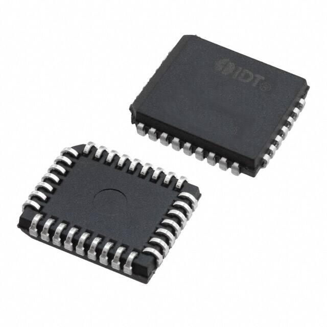
Available in 32-pin PLCC
Industrial temperature range (–40°°C to +85°°C) is available
Green parts available, see ordering information
The IDT72V01/72V02/72V03/72V04/72V05/72V06 are dual-port FIFO
memories that operate at a power supply voltage (Vcc) between 3.0V and 3.6V.
Their architecture, functional operation and pin assignments are identical to
those of the IDT7201/7202/7203/7204/7205/7206. These devices load and
empty data on a first-in/first-out basis. They use Full and Empty flags to prevent
data overflow and underflow and expansion logic to allow for unlimited
expansion capability in both word size and depth.
The reads and writes are internally sequential through the use of ring
pointers, with no address information required to load and unload data. Data
is toggled in and out of the devices through the use of the Write (W) and Read
(R) pins. The devices have a maximum data access time as fast as 25 ns.
The devices utilize a 9-bit wide data array to allow for control and parity bits
at the user’s option. This feature is especially useful in data communications
applications where it is necessary to use a parity bit for transmission/reception
error checking. They also feature a Retransmit (RT) capability that allows for
reset of the read pointer to its initial position when RT is pulsed LOW to allow for
retransmission from the beginning of data. A Half-Full Flag is available in the
single device mode and width expansion modes.
These FIFOs are fabricated using high-speed CMOS technology. It has
been designed for those applications requiring asynchronous and simultaneous read/writes in multiprocessing and rate buffer applications.
FUNCTIONAL BLOCK DIAGRAM
DATA INPUTS
(D0-D8)
W
WRITE
CONTROL
WRITE
POINTER
R
READ
CONTROL
THREESTATE
BUFFERS
DATA OUTPUTS
(Q0-Q8)
FLAG
LOGIC
XI
RAM
ARRAY
512 x 9
1,024 x 9
2,048 x 9
4,096 x 9
8,192 x 9
16,384 x 9
EF
FF
EXPANSION
LOGIC
XO/HF
IDT and the IDT logo are trademarks of Integrated Device Technology, Inc
COMMERCIAL AND INDUSTRIAL TEMPERATURE RANGES
READ
POINTER
RS
RESET
LOGIC
FL/RT
3033 drw 01
NOVEMBER 2017
1
©2017 Integrated Device Technology, Inc. All rights reserved. Product specifications subject to change without notice.
DSC-3033/8
�IDT72V01/72V02/72V03/72V04/72V05/72V06 3.3V ASYNCHRONOUS FIFO
512 x 9, 1,024 x 9, 2,048 x 9, 4,096 x 9, 8,192 x 9 and 16,384 x 9
ABSOLUTE MAXIMUM RATINGS
4 3 2
1
D5
VCC
D4
W
NC
D3
D8
PIN CONFIGURATION
INDEX
32 31 30
D2
5
29
D6
D1
6
D7
D0
XI
7
28
27
FF
8
9
26
25
Q0
10
24
FL/RT
RS
EF
Q1
11
NC
Q2
12
23
22
XO/HF
Q7
13
21
Q6
NC
Rating
Terminal Voltage
with Respect to GND
Com'l & Ind'l
–0.5 to +7.0
Unit
V
TSTG
IOUT
Storage Temperature
DC Output Current
–55 to +125
–50 to +50
°C
mA
RECOMMENDED DC OPERATING
CONDITIONS
Symbol
VCC
GND
VIH(1)
VIL(2)
Q4
Q5
NC
R
Q8
GND
Symbol
VTERM
NOTE:
1. Stresses greater than those listed under ABSOLUTE MAXIMUM RATINGS may cause
permanent damage to the device. This is a stress rating only and functional operation
of the device at these or any other conditions above those indicated in the operational
sections of this specification is not implied. Exposure to absolute maximum rating
conditions for extended periods may affect reliability.
14 15 16 17 18 19 20
Q3
COMMERCIAL AND INDUSTRIAL
TEMPERATURE RANGES
3033 drw 02b
Rating
Supply Voltage
Supply Voltage
Input High Voltage
Input Low Voltage
Min.
3.0
0
2.0
—
TA
Operating Temperature Commercial
TA
Operating Temperature Industrial
Typ. Max.
3.3
3.6
0
0
— VCC+0.5
—
0.8
0
—
70
–40
—
85
Unit
V
V
V
V
°C
°C
NOTES:
1. For RT/RS/XI input, VIH = 2.6V (commercial).
For RT/RS/XI input, VIH = 2.8V (military).
2. 1.5V undershoots are allowed for 10ns once per cycle.
PLCC (J32-1, order code: J)
TOP VIEW
DC ELECTRICAL CHARACTERISTICS
(Commercial: VCC = 3.3V ± 0.3V, TA = 0°C to +70°C; Industrial: VCC = 3.3V ± 0.3V, TA = –40°C to +85°C)
IDT72V01
IDT72V02
IDT72V03
IDT72V04
Commercial & Industrial(1)
tA = 15, 25, 35 ns
Symbol
ILI(2)
ILO(3)
VOH
VOL
ICC1(4,5)
ICC2(4,6)
Parameter
Input Leakage Current (Any Input)
Output Leakage Current
Output Logic “1” Voltage IOH = –2mA
Output Logic “0” Voltage IOL = 8mA
Active Power Supply Current
Standby Current (R=W=RS=FL/RT=VIH)
Min.
–1
–10
2.4
—
—
—
Max.
1
10
—
0.4
60
5
IDT72V05
IDT72V06
Commercial & Industrial(1)
tA = 15, 25, 35 ns
Min.
–1
–10
2.4
—
—
—
Max.
1
10
—
0.4
75
5
NOTES:
1. Industrial temperature range product for the 25ns speed grade is available as a standard device. All other speed grades are available by special order.
2. Measurements with 0.4 ≤ VIN ≤ VCC.
3. R ≥ VIH, 0.4 ≤ VOUT ≤ VCC.
4. Tested with outputs open (IOUT = 0).
5. Tested at f = 20 MHz.
6. All Inputs = VCC - 0.2V or GND + 0.2V.
CAPACITANCE (TA = +25°C, f = 1.0 MHz)
Symbol
CIN
COUT
Parameter(1)
Input Capacitance
Output Capacitance
Condition
VIN = 0V
VOUT = 0V
Max.
8
8
Unit
pF
pF
NOTE:
1. Characterized values, not currently tested.
2
Unit
µA
µA
V
V
mA
mA
�COMMERCIAL AND INDUSTRIAL
TEMPERATURE RANGES
IDT72V01/72V02/72V03/72V04/72V05/72V06 3.3V ASYNCHRONOUS FIFO
512 x 9, 1,024 x 9, 2,048 x 9, 4,096 x 9, 8,192 x 9 and 16,384 x 9
AC ELECTRICAL CHARACTERISTICS(1)
(Commercial: VCC = 3.3V ± 0.3V, TA = 0°C to +70°C; Industrial: VCC = 3.3V ± 0.3V, TA = –40°C to +85°C)
Symbol
fS
tRC
tA
tRR
tRPW
tRLZ
tWLZ
tDV
tRHZ
tWC
tWPW
tWR
tDS
tDH
tRSC
tRS
tRSS
tRSR
tRTC
tRT
tRTS
tRTR
tEFL
tHFH,FFH
tRTF
tREF
tRFF
tRPE
tWEF
tWFF
tWHF
tRHF
tWPF
tXOL
tXOH
tXI
tXIR
tXIS
Parameter
Shift Frequency
Read Cycle Time
Access Time
Read Recovery Time
Read Pulse Width(3)
Read Pulse Low to Data Bus at Low Z(4)
Write Pulse High to Data Bus at Low Z(4,5)
Data Valid from Read Pulse High
Read Pulse High to Data Bus at High Z(4)
Write Cycle Time
Write Pulse Width(3)
Write Recovery Time
Data Setup Time
Data Hold Time
Reset Cycle Time
Reset Pulse Width(3)
Reset Setup Time(4)
Reset Recovery Time
Retransmit Cycle Time
Retransmit Pulse Width(3)
Retransmit Setup Time(4)
Retransmit Recovery Time
Reset to Empty Flag Low
Reset to Half-Full and Full Flag High
Retransmit Low to Flags Valid
Read Low to Empty Flag Low
Read High to Full Flag High
Read Pulse Width after EF High
Write High to Empty Flag High
Write Low to Full Flag Low
Write Low to Half-Full Flag Low
Read High to Half-Full Flag High
Write Pulse Width after FF High
Read/Write to XO Low
Read/Write to XO High
XI Pulse Width(3)
XI Recovery Time
XI Setup Time
Commercial
IDT72V01L15
IDT72V02L15
IDT72V03L15
IDT72V04L15
IDT72V05L15
IDT72V06L15
Min.
Max.
—
40
25
—
—
15
10
—
15
—
3
—
5
—
5
—
—
15
25
—
15
—
10
—
11
—
0
—
25
—
15
—
15
—
10
—
25
—
15
—
15
—
10
—
—
25
—
25
—
25
—
15
—
15
15
—
—
15
—
15
—
25
—
25
15
—
—
15
—
15
15
—
10
—
10
—
NOTES:
1. Timings referenced as in AC Test Conditions.
2. Industrial temperature range product for the 25ns speed grade is available as a standard device.
All other speed grades are available by special order.
3. Pulse widths less than minimum value are not allowed.
4. Values guaranteed by design, not currently tested.
5. Only applies to read data flow-through mode.
AC TEST CONDITIONS
Input Pulse Levels
Input Rise/Fall Times
Input Timing Reference Levels
Output Reference Levels
Output Load
Com'l and Ind'l(2)
IDT72V01L25
IDT72V02L25
IDT72V03L25
IDT72V04L25
IDT72V05L25
IDT72V06L25
Min.
Max.
—
28.5
35
—
—
25
10
—
25
—
3
—
5
—
5
—
—
18
35
—
25
—
10
—
15
—
0
—
35
—
25
—
25
—
10
—
35
—
25
—
25
—
10
—
—
35
—
35
—
35
—
25
—
25
25
—
—
25
—
25
—
35
—
35
25
—
—
25
—
25
25
—
10
—
10
—
Commercial
IDT72V01L35
IDT72V02L35
IDT72V03L35
IDT72V04L35
IDT72V05L35
IDT72V06L35
Min.
Max.
—
22.2
45
—
—
35
10
—
35
—
3
—
5
—
5
—
—
20
45
—
35
—
10
—
18
—
0
—
45
—
35
—
35
—
10
—
45
—
35
—
35
—
10
—
—
45
—
45
—
45
—
30
—
30
35
—
—
30
—
30
—
45
—
45
35
—
—
35
—
35
35
—
10
—
10
—
3.3V
330Ω
D.U.T.
510Ω
GND to 3.0V
5ns
1.5V
1.5V
See Figure 1
30pF*
3033 drw 03
or equivalent circuit
Figure 1. Output Load
* Includes scope and jig capacitances.
3
Unit
MHz
ns
ns
ns
ns
ns
ns
ns
ns
ns
ns
ns
ns
ns
ns
ns
ns
ns
ns
ns
ns
ns
ns
ns
ns
ns
ns
ns
ns
ns
ns
ns
ns
ns
ns
ns
ns
ns
�IDT72V01/72V02/72V03/72V04/72V05/72V06 3.3V ASYNCHRONOUS FIFO
512 x 9, 1,024 x 9, 2,048 x 9, 4,096 x 9, 8,192 x 9 and 16,384 x 9
SIGNAL DESCRIPTIONS
COMMERCIAL AND INDUSTRIAL
TEMPERATURE RANGES
FIRST LOAD/RETRANSMIT (FL/RT)
This is a dual-purpose input. In the Depth Expansion Mode, this pin is
grounded to indicate that it is the first loaded (see Operating Modes). In the Single
Device Mode, this pin acts as the retransmit input. The Single Device Mode is
initiated by grounding the Expansion In (XI).
These FIFOs can be made to retransmit data when the Retransmit Enable
control (RT) input is pulsed LOW. A retransmit operation will set the internal read
pointer to the first location and will not affect the write pointer. Read Enable (R)
and Write Enable (W) must be in the HIGH state during retransmit. This feature
is useful when less than 512/1,024/2,048/4,096/8,192/16,384 writes are
performed between resets. The retransmit feature is not compatible with the
Depth Expansion Mode and will affect the Half-Full Flag (HF), depending on
the relative locations of the read and write pointers.
INPUTS:
DATA IN (D0 – D8)
Data inputs for 9-bit wide data.
CONTROLS:
RESET (RS)
Reset is accomplished whenever the Reset (RS) input is taken to a LOW
state. During reset, both internal read and write pointers are set to the first
location. A reset is required after power up before a write operation can take
place. Both the Read Enable (R) and Write Enable (W) inputs must be
in the HIGH state during the window shown in Figure 2, (i.e., tRSS
before the rising edge of RS ) and should not change until tRSR after
the rising edge of RS. Half-Full Flag (HF) will be reset to HIGH after
Reset (RS).
EXPANSION IN (XI)
This input is a dual-purpose pin. Expansion In (XI) is grounded to indicate
an operation in the single device mode. Expansion In (XI) is connected to
Expansion Out (XO) of the previous device in the Depth Expansion or Daisy
Chain Mode.
WRITE ENABLE (W)
A write cycle is initiated on the falling edge of this input if the Full Flag (FF)
is not set. Data setup and hold times must be adhered to with respect to the rising
edge of the Write Enable (W). Data is stored in the RAM array sequentially and
independently of any ongoing read operation.
After half of the memory is filled and at the falling edge of the next write
operation, the Half-Full Flag (HF) will be set to LOW and will remain set until the
difference between the write pointer and read pointer is less than or equal to
one half of the total memory of the device. The Half-Full Flag (HF) is then reset
by the rising edge of the read operation.
To prevent data overflow, the Full Flag (FF) will go LOW, inhibiting further
write operations. Upon the completion of a valid read operation, the Full Flag
(FF) will go HIGH after tRFF, allowing a valid write to begin. When the FIFO
is full, the internal write pointer is blocked from W, so external changes in W will
not affect the FIFO when it is full.
OUTPUTS:
FULL FLAG (FF)
The Full Flag (FF) will go LOW, inhibiting further write operation, when the
write pointer is one location less than the read pointer, indicating that the device
is full. If the read pointer is not moved after Reset (RS), the Full-Flag (FF) will
go LOW after 512/1,024/2,048/4,096/8,192/16,384 writes to the IDT72V01/
72V02/72V03/72V04/72V05/72V06.
EMPTY FLAG (EF)
The Empty Flag (EF) will go LOW, inhibiting further read operations, when
the read pointer is equal to the write pointer, indicating that the device is empty.
EXPANSION OUT/HALF-FULL FLAG (XO/HF)
This is a dual-purpose output. In the single device mode, when Expansion
In (XI) is grounded, this output acts as an indication of a half-full memory.
After half of the memory is filled and at the falling edge of the next write
operation, the Half-Full Flag (HF) will be set LOW and will remain set until the
difference between the write pointer and read pointer is less than or equal to
one half of the total memory of the device. The Half-Full Flag (HF) is then reset
by using rising edge of the read operation.
In the Depth Expansion Mode, Expansion In (XI) is connected to Expansion
Out (XO) of the previous device. This output acts as a signal to the next device
in the Daisy Chain by providing a pulse to the next device when the previous
device reaches the last location of memory.
READ ENABLE (R)
A read cycle is initiated on the falling edge of the Read Enable (R) provided
the Empty Flag (EF) is not set. The data is accessed on a First-In/First-Out basis,
independent of any ongoing write operations. After Read Enable (R) goes
HIGH, the Data Outputs (Q0 – Q8) will return to a high impedance condition until
the next Read operation. When all data has been read from the FIFO, the Empty
Flag (EF) will go LOW, allowing the “final” read cycle but inhibiting further read
operations with the data outputs remaining in a high impedance state. Once a
valid write operation has been accomplished, the Empty Flag (EF) will go HIGH
after tWEF and a valid Read can then begin. When the FIFO is empty, the internal
read pointer is blocked from R so external changes in R will not affect the FIFO
when it is empty.
DATA OUTPUTS (Q0 – Q8)
Data outputs for 9-bit wide data. This data is in a high impedance condition
whenever Read (R) is in a HIGH state.
4
�COMMERCIAL AND INDUSTRIAL
TEMPERATURE RANGES
IDT72V01/72V02/72V03/72V04/72V05/72V06 3.3V ASYNCHRONOUS FIFO
512 x 9, 1,024 x 9, 2,048 x 9, 4,096 x 9, 8,192 x 9 and 16,384 x 9
tRSC
tRS
RS
tRSR
tRSS
W
tRSS
R
tEFL
EF
tHFH, tFFH
HF, FF
3033 drw 04
NOTES:
1. EF, FF, HF may change status during Reset, but flags will be valid at tRSC.
2. W and R = VIH around the rising edge of RS.
Figure 2. Reset
tRC
tRPW
tRR
tA
tA
R
tDV
tRLZ
Q0-Q8
tRHZ
DATA OUT VALID
tWC
tWPW
DATA OUT VALID
tWR
W
tDS
D0-D8
tDH
DATA IN VALID
DATA IN VALID
3033 drw 05
Figure 3. Asynchronous Write and Read Operation
LAST WRITE
IGNORED
WRITE
FIRST READ
ADDITIONAL
READS
FIRST
WRITE
R
W
tWFF
t RFF
FF
3033 drw 06
Figure 4. Full Flag From Last Write to First Read
5
�IDT72V01/72V02/72V03/72V04/72V05/72V06 3.3V ASYNCHRONOUS FIFO
512 x 9, 1,024 x 9, 2,048 x 9, 4,096 x 9, 8,192 x 9 and 16,384 x 9
LAST READ
IGNORED
READ
FIRST WRITE
ADDITIONAL
WRITES
COMMERCIAL AND INDUSTRIAL
TEMPERATURE RANGES
FIRST
READ
W
R
t WEF
t REF
EF
tA
DATA OUT
VALID
VALID
3033 drw 07
Figure 5. Empty Flag From Last Read to First Write
t RTC
tRT
RT
t RTS
tRTR
W,R
t RTF
HF, EF, FF
FLAG VALID
3033 drw 08
Figure 6. Retransmit
W
tWEF
EF
tRPE
R
3033 drw 09
Figure 7. Minimum Timing for an Empty Flag Coincident Read Pulse
R
t RFF
FF
t WPF
W
3033 drw 10
Figure 8. Minimum Timing for a Full Flag Coincident Write Pulse
6
�COMMERCIAL AND INDUSTRIAL
TEMPERATURE RANGES
IDT72V01/72V02/72V03/72V04/72V05/72V06 3.3V ASYNCHRONOUS FIFO
512 x 9, 1,024 x 9, 2,048 x 9, 4,096 x 9, 8,192 x 9 and 16,384 x 9
W
tRHF
R
tWHF
HF
HALF-FULL OR LESS
HALF-FULL OR LESS
MORE THAN HALF-FULL
3033 drw 11
Figure 9. Half-Full Flag Timing
WRITE TO
LAST PHYSICAL
LOCATION
W
READ FROM
LAST PHYSICAL
LOCATION
R
t XOH
t XOL
t XOL
t XOH
3033 drw 12
XO
Figure 10. Expansion Out
t XI
t XIR
XI
t XIS
W
WRITE TO
FIRST PHYSICAL
LOCATION
t XIS
READ FROM
FIRST PHYSICAL
LOCATION
R
Figure 11. Expansion In
7
3033 drw 13
�IDT72V01/72V02/72V03/72V04/72V05/72V06 3.3V ASYNCHRONOUS FIFO
512 x 9, 1,024 x 9, 2,048 x 9, 4,096 x 9, 8,192 x 9 and 16,384 x 9
COMMERCIAL AND INDUSTRIAL
TEMPERATURE RANGES
USAGE MODES:
OPERATING MODES:
Care must be taken to assure that the appropriate flag is monitored by each
system (i.e. FF is monitored on the device where W is used; EF is monitored
on the device where R is used). For additional information, refer to Tech Note
8: Operating FIFOs on Full and Empty Boundary Conditions and Tech Note
6: Designing with FIFOs.
WIDTH EXPANSION
Word width may be increased simply by connecting the corresponding input
control signals of multiple devices. Status flags (EF, FF and HF) can be detected
from any one device. Figure 13 demonstrates an 18-bit word width by using
two IDT72V01/72V02/72V03/72V04/72V05/72V06s. Any word width can be
attained by adding additional IDT72V01/72V02/72V03/72V04/72V05/72V06s
(Figure 13).
SINGLE DEVICE MODE
A single IDT72V01/72V02/72V03/72V04/72V05/72V06 may be used
when the application requirements are for 512/1,024/2,048/4,096/8,192/
16,384 words or less. These devices are in a Single Device Configuration when
the Expansion In ( XI ) control input is grounded (see Figure 12).
These FIFOs can easily be adapted to applications when the requirements
are for greater than 512/1,024/2,048/4,096/8,192/16,384 words. Figure 14
demonstrates Depth Expansion using three IDT72V01/72V02/72V03/72V04/
72V05/72V06s. Any depth can be attained by adding additional IDT72V01/
72V02/72V03/72V04/72V05/72V06s. These devices operate in the Depth
Expansion mode when the following conditions are met:
BIDIRECTIONAL OPERATION
Applications which require data buffering between two systems (each
system capable of Read and Write operations) can be achieved by pairing
IDT72V01/72V02/72V03/72V04/72V05/72V06s as shown in Figure 16. Both
Depth Expansion and Width Expansion may be used in this mode.
DATA FLOW-THROUGH
Two types of flow-through modes are permitted, a read flow-through and
write flow-through mode. For the read flow-through mode (Figure 17), the FIFO
permits a reading of a single word after writing one word of data into an empty
FIFO. The data is enabled on the bus in (tWEF + tA) ns after the rising edge of
W, called the first write edge, and it remains on the bus until the R line is raised
from LOW-to-HIGH, after which the bus would go into a three-state mode after
tRHZ ns. The EF line would have a pulse showing temporary deassertion and
then would be asserted.
In the write flow-through mode (Figure 18), the FIFO permits the writing of
a single word of data immediately after reading one word of data from a full FIFO.
The R line causes the FF to be deasserted but the W line being LOW causes
it to be asserted again in anticipation of a new data word. On the rising edge
of W, the new word is loaded in the FIFO. The W line must be toggled when FF
is not asserted to write new data in the FIFO and to increment the write pointer.
1. The first device must be designated by grounding the First Load ( FL) control
input.
2. All other devices must have FL in the HIGH state.
3. The Expansion Out ( XO) pin of each device must be tied to the Expansion
In ( XI ) pin of the next device. See Figure 14.
4. External logic is needed to generate a composite Full Flag ( FF) and Empty
Flag ( EF ). This requires the ORing of all EFs and ORing of all FFs (i.e.
all must be set to generate the correct composite FF or EF). See Figure 14.
5. The Retransmit ( RT ) function and Half-Full Flag ( HF ) are not available
in the Depth Expansion Mode.
For additional information, refer to Tech Note 9: Cascading FIFOs or FIFO
Modules.
8
�COMMERCIAL AND INDUSTRIAL
TEMPERATURE RANGES
IDT72V01/72V02/72V03/72V04/72V05/72V06 3.3V ASYNCHRONOUS FIFO
512 x 9, 1,024 x 9, 2,048 x 9, 4,096 x 9, 8,192 x 9 and 16,384 x 9
(HALF-FULL FLAG)
(HF)
WRITE (W)
IDT
72V01
72V02
72V03
72V04
72V05
72V06
9
DATA IN (D)
FULL FLAG (FF)
RESET (RS)
READ (R)
9
DATA OUT (Q)
EMPTY FLAG (EF)
RETRANSMIT (RT)
3033 drw 14
EXPANSION IN (XI)
Figure 12. Block Diagram of Single 512 x 9, 1,024 x 9, 2,048 x 9, 4,096 x 9, 8,192 x 9 and 16,384 x 9 FIFO
HF
HF
18
9
9
DATA IN (D)
IDT
72V01
72V02
72V03
72V04
72V05
72V06
WRITE (W)
FULL FLAG (FF)
RESET (RS)
IDT
72V01
72V02
72V03
72V04
72V05
72V06
9
XI
READ (R)
EMPTY FLAG (EF)
RETRANSMIT (RT)
9
XI
18
DATA
OUT(Q)
3033 drw 15
Figure 13. Block Diagram of 512 x 18, 1,024 x 18, 2,048 x 18, 4,096 x 18, 8,192 x 18 and 16,384 x 18 FIFO Memory Used in Width Expansion Mode
TABLE 1 — RESET AND RETRANSMIT
Single Device Configuration/Width Expansion Mode
Reset
Retransmit
RS
0
1
Inputs
RT
X
0
Read/Write
1
1
Mode
XI
0
0
Internal Status
Read Pointer
Write Pointer
Location Zero
Location Zero
Location Zero
Unchanged
0
Increment(1)
NOTE:
1. Pointer will increment if flag is HIGH
9
Increment(1)
EF
0
X
X
Outputs
FF
1
X
X
HF
1
X
X
�IDT72V01/72V02/72V03/72V04/72V05/72V06 3.3V ASYNCHRONOUS FIFO
512 x 9, 1,024 x 9, 2,048 x 9, 4,096 x 9, 8,192 x 9 and 16,384 x 9
COMMERCIAL AND INDUSTRIAL
TEMPERATURE RANGES
TABLE 2 — RESET AND FIRST LOAD TRUTH TABLE
Depth Expansion/Compound Expansion Mode
Mode
Reset First Device
Reset All Other Devices
Read/Write
RS
0
0
Inputs
FL
0
1
XI
(1)
(1)
1
X
(1)
Read Pointer
Location Zero
Location Zero
Internal Status
Write Pointer
Location Zero
Location Zero
X
X
Outputs
EF
0
0
FF
1
1
X
X
NOTE:
1. XI is connected to XO of previous device. See Figure 14. RS = Reset Input, FL/RT = First Load/Retransmit, EF = Empty Flag Output, FF = Full Flag Output,
XI = Expansion Input, HF = Half-Full Flag Output
XO
W
D
FF
9
9
IDT
72V01
72V02
72V03
72V04
72V05
72V06
R
EF
9
FL
Q
VCC
XI
XO
FF
FULL
9
IDT
72V01
72V02
72V03
72V04
72V05
72V06
EF
EMPTY
FL
XI
XO
FF
9
RS
IDT
72V01
72V02
72V03
72V04
72V05
72V06
XI
EF
FL
Figure 14. Block Diagram of 1,536 x 9, 3,072 x 9, 6,144 x 9, 12,288 x 9, 24,576 x 9 and 49,152 x 9 FIFO Memory (Depth Expansion)
Q0-Q8
R, W, RS
Q9-Q17
IDT
72V01/72V02/72V03/
72V04/72V05/72V06
DEPTH
EXPANSION
BLOCK
IDT
72V01/72V02/72V03/
72V04/72V05/72V06
DEPTH
EXPANSION
BLOCK
D0-D8
D9-D17
Q(N-8)-QN
IDT
72V01/72V02/72V03/
72V04/72V05/72V06
DEPTH
EXPANSION
BLOCK
D(N-8)-DN
D0-DN
NOTES:
1. For depth expansion block see section on Depth Expansion and Figure 14.
2. For Flag detection see section on Width Expansion and Figure 13.
3033 drw 17
Figure 15. Compound FIFO Expansion
10
�COMMERCIAL AND INDUSTRIAL
TEMPERATURE RANGES
IDT72V01/72V02/72V03/72V04/72V05/72V06 3.3V ASYNCHRONOUS FIFO
512 x 9, 1,024 x 9, 2,048 x 9, 4,096 x 9, 8,192 x 9 and 16,384 x 9
WA
FFA
IDT
72V01
72V02
IDT
72V03
7201A
72V04
72V05
72V06
DA 0-8
RB
EFB
HFB
QB 0-8
SYSTEM A
SYSTEM B
QA 0-8
RA
HFA
EFA
IDT
72V01
72V02
72V03
72V04
72V05
72V06
DB 0-8
WB
FFB
3033 drw 18
Figure 16. Bidirectional FIFO Mode
DATA
IN
W
t RPE
R
EF
t WLZ
t WEF
tA
t REF
DATA OUT
DATA
OUT VALID
3033 drw 19
Figure 17. Read Data Flow-Through Mode
R
tWPF
W
tRFF
FF
tDH
tWFF
DATA
DATA IN
tA
DATA OUT
IN
VALID
t DS
DATA
OUT
VALID
3033 drw 20
Figure 18. Write Data Flow-Through Mode
11
�ORDERING INFORMATION
XXXXX
X
XXX
X
Device Type Power Speed Package
X
X
X
Process/
Temperature
Range
Blank
8
Tube or Tray
Tape and Reel
Blank
I(1)
Commercial (0°C to +70°C)
Industrial (-40°C to +85°C)
G(2)
Green
J
Plastic Leaded Chip Carrier (PLCC, J32-1)
15
25
35
Commercial Only
Com'l and Ind'l
Commercial Only
L
Low Power
72V01
72V02
72V03
72V04
72V05
72V06
512 x 9 FIFO
1,024 x 9 FIFO
2,048 x 9 FIFO
4,096 x 9 FIFO
8,192 x 9 FIFO
16,384 x 9 FIFO
Access Time (tA)
Speed in Nanoseconds
3033 drw 21
NOTES:
1. Industrial temperature range product for the 25ns speed grade is available as a standard device. All other speed grades are available by special order.
2. Green parts are available. For specific speeds and packages contact your local sales office.
LEAD FINISH (SnPb) parts are in EOL process. Product Discontinuation Notice - PDN# SP-17-02
DATASHEET DOCUMENT HISTORY
08/29/2001
04/08/2003
05/05/2003
03/09/2006
10/22/2008
06/29/2012
11/27/2017
pg. 3.
pg. 2.
pg. 2.
pgs. 1 and 12.
pgs. 12.
pgs. 1 and 12.
Product Discontinuation Notice - PDN# SP-17-02
Last time buy expires June 15, 2018.
CORPORATE HEADQUARTERS
6024 Silver Creek Valley Road
San Jose, CA 95138
for SALES:
800-345-7015 or 408-284-8200
fax: 408-284-2775
www.idt.com
12
for Tech Support:
408-360-1753
email: FIFOhelp@idt.com
�IMPORTANT NOTICE AND DISCLAIMER
RENESAS ELECTRONICS CORPORATION AND ITS SUBSIDIARIES (“RENESAS”) PROVIDES TECHNICAL
SPECIFICATIONS AND RELIABILITY DATA (INCLUDING DATASHEETS), DESIGN RESOURCES (INCLUDING
REFERENCE DESIGNS), APPLICATION OR OTHER DESIGN ADVICE, WEB TOOLS, SAFETY INFORMATION, AND
OTHER RESOURCES “AS IS” AND WITH ALL FAULTS, AND DISCLAIMS ALL WARRANTIES, EXPRESS OR IMPLIED,
INCLUDING, WITHOUT LIMITATION, ANY IMPLIED WARRANTIES OF MERCHANTABILITY, FITNESS FOR A
PARTICULAR PURPOSE, OR NON-INFRINGEMENT OF THIRD PARTY INTELLECTUAL PROPERTY RIGHTS.
These resources are intended for developers skilled in the art designing with Renesas products. You are solely responsible
for (1) selecting the appropriate products for your application, (2) designing, validating, and testing your application, and (3)
ensuring your application meets applicable standards, and any other safety, security, or other requirements. These
resources are subject to change without notice. Renesas grants you permission to use these resources only for
development of an application that uses Renesas products. Other reproduction or use of these resources is strictly
prohibited. No license is granted to any other Renesas intellectual property or to any third party intellectual property.
Renesas disclaims responsibility for, and you will fully indemnify Renesas and its representatives against, any claims,
damages, costs, losses, or liabilities arising out of your use of these resources. Renesas' products are provided only subject
to Renesas' Terms and Conditions of Sale or other applicable terms agreed to in writing. No use of any Renesas resources
expands or otherwise alters any applicable warranties or warranty disclaimers for these products.
(Rev.1.0 Mar 2020)
Corporate Headquarters
Contact Information
TOYOSU FORESIA, 3-2-24 Toyosu,
Koto-ku, Tokyo 135-0061, Japan
www.renesas.com
For further information on a product, technology, the most
up-to-date version of a document, or your nearest sales
office, please visit:
www.renesas.com/contact/
Trademarks
Renesas and the Renesas logo are trademarks of Renesas
Electronics Corporation. All trademarks and registered
trademarks are the property of their respective owners.
© 2020 Renesas Electronics Corporation. All rights reserved.
�