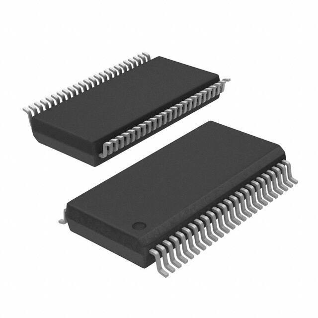
IDT74CBTLV16800
LOW-VOLTAGE 20-BIT BUS SWITCH WITH PRECHARGED OUTPUTS
INDUSTRIAL TEMPERATURE RANGE
LOW-VOLTAGE 20-BIT
BUS SWITCH WITH
PRECHARGED OUTPUTS
IDT74CBTLV16800
FEATURES:
DESCRIPTION:
•
•
•
•
•
•
The CBTLV16800 provides 20-bits of high-speed bus switching with low
on-state resistance of the switch allowing connections to be made with
minimal propagation delay. The device also precharges the B port to a
user-selectable bias voltage (BIASV) to minimize live-insertion noise.
The CBTLV16800 is organized as dual 10-bit bus switches with two
different output-enable (OE) control inputs. When OE is low, the corresponding 10-bit bus switch is on and port A is connected to port B. When
OE is high, the switch is open, and a high impedance state exists between
the two ports, and port B is precharged to BIASV through the equivalent
of a 10-kΩ resistor.
To ensure the high-impedance state during power up or power down,
OE should be tied to VCC through a pullup resistor; the minimum value of
the resistor is determined by the current-sinking capability of the driver.
5Ω
Ω A/B bi-directional switch
Isolation Under Power-Off Conditions
Over-voltage tolerant
Latch-up performance exceeds 100mA
VCC = 2.3V - 3.6V, normal range
ESD >2000V per MIL-STD-883, Method 3015; >200V using
machine model (C = 200pF, R = 0)
• Available in TSSOP and TVSOP packages
APPLICATIONS:
• 3.3V High Speed Bus Switching and Bus Isolation
FUNCTIONAL BLOCK DIAGRAM
1
1A1
1A10
1OE
2A1
2
12
SW
SW
46
36
SIMPLIFIED SCHEMATIC, EACH
SWITCH
BIASV
1B1
1B10
A
B
48
13
SW
35
2B1
OE
2A10
2OE
24
SW
25
2B10
1
The IDT logo is a registered trademark of Integrated Device Technology, Inc.
INDUSTRIAL TEMPERATURE RANGE
JUNE 2006
1
c
2006 Integrated Device Technology, Inc.
DSC-5886/9
�IDT74CBTLV16800
LOW-VOLTAGE 20-BIT BUS SWITCH WITH PRECHARGED OUTPUTS
PIN CONFIGURATION
INDUSTRIAL TEMPERATURE RANGE
ABSOLUTE MAXIMUM RATINGS(1)
Symbol
BIASV
1
48
V
Bias Voltage Range, VI
–0.5 to 4.6
V
Input Voltage Range
–0.5 to 4.6
V
BIASV
VI
47
2OE
1A 2
3
46
1B 1
4
45
1B 2
1A 4
5
44
1B3
1A 5
6
43
1B4
1A 6
7
42
1B5
GND
8
41
GND
1A 7
9
40
1B6
1A 8
10
39
1B7
1A 9
11
38
1B8
1A 10
12
37
1B9
2A 1
13
36
1B 10
14
35
2B1
VCC
15
34
2B 2
2A 3
16
33
2B3
GND
17
32
2A 4
18
31
GND
2B 4
2A 5
19
30
2B 5
2A 6
20
29
2B 6
2A 7
21
28
2B 7
2A 8
22
27
2B 8
2A 9
23
26
2B9
24
25
2B10
2A 10
Unit
1OE
2
2A 2
Max.
–0.5 to 4.6
Supply Voltage Range
1A 1
1A 3
Description
VCC
IIK
TSTG
Continuous Channel Current
128
mA
Input Clamp Current, VI/O < 0
–50
mA
–65 to +150
°C
Storage Temperature Range
NOTE:
1. Stresses greater than those listed under ABSOLUTE MAXIMUM RATINGS may cause
permanent damage to the device. This is a stress rating only and functional operation
of the device at these or any other conditions above those indicated in the operational
sections of this specification is not implied. Exposure to absolute maximum rating
conditions for extended periods may affect reliability.
FUNCTION TABLE (EACH 10-BIT BUS SWITCH)(1)
Input OE
Inputs/Outputs
L
A-Port = B-Port
H
A-Port = Z
B-Port = BIASV
NOTE:
1. H = HIGH Voltage Level
L = LOW Voltage Level
Z = High-Impedance
TSSOP/ TVSOP
TOP VIEW
OPERATING CHARACTERISTICS(1)
Symbol
VCC
BIASV
VIH
VIL
TA
Parameter
Test Conditions
Supply Voltage
Bias Voltage
High-Level Control Input Voltage
Low-Level Control Input Voltage
Min.
Max.
Unit
2.3
3.6
V
1.3
VCC
V
VCC = 2.3V to 2.7V
1.7
—
V
VCC = 2.7V to 3.6V
2
—
VCC = 2.3V to 2.7V
—
0.7
VCC = 2.7V to 3.6V
—
0.8
–40
+85
Operating Free-Air Temperature
NOTE:
1. All unused control inputs of the device must be held at VCC or GND to ensure proper device operation.
2
V
°C
�IDT74CBTLV16800
LOW-VOLTAGE 20-BIT BUS SWITCH WITH PRECHARGED OUTPUTS
INDUSTRIAL TEMPERATURE RANGE
DC ELECTRICAL CHARACTERISTICS OVER OPERATING RANGE
Following Conditions Apply Unless Otherwise Specified:
Operating Condition: TA = –40°C to +85°C
Symbol
VIK
Parameter
Test Conditions
Min.
Typ.
Max.
Unit
Control Inputs, Data I/O
VCC = 3V, II = –18mA
—
—
–1.2
V
Control Inputs
VCC = 3.6V, VI = VCC or GND
—
—
±1
µA
IOZ
Data I/O
VCC = 3.6V, VO = 0V or 3.6V switch disabled
—
—
5
µA
I OFF
A Port
—
—
10
µA
| 0.25 |
—
—
mA
II
VCC = 0V, VI or VO = 0V or 3.6V
VCC = 3V, BIASV = 2.4V, VO = 0, OE = VCC
IO
VCC = 3.6V, IO = 0, VI = VCC or GND
—
—
10
µA
ΔICC(1)
ICC
Control Inputs
VCC = 3.6V, one input at 3V, other inputs at VCC or GND
—
—
300
µA
CI
Control Inputs
VI = 3V or 0
—
4
—
pF
VO = 3V or 0, switch off, BIASV = open, OE = VCC
—
6.5
—
pF
VI = 0
II = 64mA
—
5
9
CIO(OFF)
VCC = 2.3V
Typ. at VCC = 2.5V
RON
II = 24mA
—
5
9
VI = 1.7V
II = 15mA
—
25
35
VI = 0
II = 64mA
—
5
7
II = 24mA
—
5
7
II = 15mA
—
10
15
VCC = 3V
VI = 2.4V
Ω
NOTES:
1. The increase in supply current is attributable to each input that is at the specified voltage level rather than VCC or GND.
2. This is measured by the voltage drop between the A and B terminals at the indicated current through the switch. On-state resistance is determined by the lower of the voltages
of the two (A or B) terminals.
SWITCHING CHARACTERISTICS
VCC = 2.5V ± 0.2V
Symbol
tPD(1)
Parameter
Propagation Delay
VCC = 3.3V ± 0.3V
Min.
Max.
Min.
Max.
Unit
—
0.15
—
0.25
ns
2.9
7.7
2.2
5.5
ns
2.8
6.4
2.1
5.3
ns
1.4
6.8
2.6
7.6
ns
1.3
4.2
1.5
5.1
ns
A to B or B to A
tPZH
BIASV = GND
OE to A or B
tPZL
BIASV = 3V
OE to A or B
tPHZ
BIASV = GND
OE to A or B
tPLZ
BIASV = 3V
OE to A or B
NOTE:
1. The propagation delay is the calculated RC time constant of the typical on-state resistance of the switch and the specified load capacitance when driven by an ideal voltage source
(zero output impededance).
3
�IDT74CBTLV16800
LOW-VOLTAGE 20-BIT BUS SWITCH WITH PRECHARGED OUTPUTS
INDUSTRIAL TEMPERATURE RANGE
TEST CIRCUITS AND WAVEFORMS
TEST CONDITIONS
Symbol
VCC(1)= 3.3V±0.3V
VCC(2)= 2.5V±0.2V
Unit
VLOAD
6
2 x Vcc
V
VIH
3
Vcc
V
VT
1.5
Vcc / 2
V
VLZ
300
150
mV
VHZ
300
150
mV
CL
50
30
pF
SAME PHASE
INPUT TRANSITION
tPLH
tPHL
tPLH
tPHL
OUTPUT
VIH
VT
0V
VOH
VT
VOL
VIH
VT
0V
OPPOSITE PHASE
INPUT TRANSITION
Propagation Delay
VLOAD
VCC
500Ω
Pulse(1, 2)
Generator
VIN
CONTROL
INPUT
GND
tPZL
VOUT
D.U.T.
RT
DISABLE
ENABLE
Open
OUTPUT
SWITCH
NORMALLY
CLOSED
LOW
tPZH
OUTPUT SWITCH
NORMALLY
OPEN
HIGH
500Ω
CL
Test Circuits for All Outputs
SWITCH POSITION
tPLZ/tPZL
VLOAD
tPHZ/tPZH
GND
tPD
Open
tPHZ
VT
0V
Enable and Disable Times
NOTES:
1. Pulse Generator for All Pulses: Rate ≤ 10MHz; tF ≤ 2.5ns; tR ≤ 2.5ns.
2. Pulse Generator for All Pulses: Rate ≤ 10MHz; tF ≤ 2ns; tR ≤ 2ns.
Switch
VLOAD/2
VT
VLOAD/2
VOL + VLZ
VOL
VOH
VOH -VHZ
0V
NOTE:
1. Diagram shown for input Control Enable-LOW and input Control Disable-HIGH.
DEFINITIONS:
CL = Load capacitance: includes jig and probe capacitance.
RT = Termination resistance: should be equal to ZOUT of the Pulse Generator.
Test
tPLZ
VIH
VT
0V
4
�IDT74CBTLV16800
LOW-VOLTAGE 20-BIT BUS SWITCH WITH PRECHARGED OUTPUTS
INDUSTRIAL TEMPERATURE RANGE
ORDERING INFORMATION
CBTLV
XXX
XX
IDT
XX
Temp. Range
Device Type Package
PVG
PA
PAG
PF
SSOP - Green
Thin Shrink Small Outline Package
TSSOP - Green
Thin Very Small Outline Package
16800 Low-Voltage 20-Bit Bus Switch with Precharged Outputs
74
CORPORATE HEADQUARTERS
6024 Silver Creek Valley Road
San Jose, CA 95138
–40°C to +85°C
for SALES:
800-345-7015 or 408-284-8200
fax: 408-284-2775
www.idt.com
5
for Tech Support:
logichelp@idt.com
�
很抱歉,暂时无法提供与“74CBTLV16800PAG”相匹配的价格&库存,您可以联系我们找货
免费人工找货