FemtoClock® Dual VCXO Video PLL
ICS810001I-21
DATASHEET
General Description
Features
The ICS810001I-21 is a PLL based synchronous clock generator
that is optimized for digital video clock jitter attenuation and
frequency translation. The device contains two internal frequency
multiplication stages that are cascaded in series. The first stage is a
VCXO PLL that is optimized to provide reference clock jitter
attenuation, and to support the complex PLL multiplication ratios
needed for video rate conversion. The second stage is a
FemtoClock® frequency multiplier that provides the low jitter, high
frequency video output clock.
•
•
Jitter attenuation and frequency translation of video clock signals
•
Support of High-Definition (HD) and Standard-Definition (SD)
pixel rates
•
Dual VCXO-PLL supports both 60 and 59.94Hz base frame rates
in one device
•
•
Supports both 1000/1001 and 1001/1000 rate conversions
•
VCXO-PLL mode for low-frequency clock generation (27MHz and
26.973MHz)
•
•
•
•
One LVCMOS/LVTTL clock output
•
•
•
3.3V supply voltage
Preset multiplication ratios are selected from internal lookup tables
using device input selection pins. The multiplication ratios are
optimized to support most common video rates used in professional
video system applications. The VCXO requires the use of an
external, inexpensive pullable crystal. Two crystal connections are
provided (pin selectable) so that both 60 and 59.94 base frame rates
can be supported. The VCXO requires external passive loop filter
components which are used to set the PLL loop bandwidth and
damping characteristics.
Supported Input Frequencies
Supports SMPTE 292M, ITU-R Rec. 601/656 and
MPEG-transport clocks
Dual PLL mode for high-frequency clock generation
(36MHz to 148.5MHz)
Two selectable LVCMOS/LVTTL clock inputs
LVCMOS/LVTTL compatible control signals
RMS phase jitter @148.3516MHz, (12kHz - 20MHz):
1.089ps (typical)
-40°C to 85°C ambient operating temperature
Lead-free (RoHS 6) packaging
Supported Output Frequencies
fVCXO = 27MHz
fVCXO = 26.973MHz
fVCXO = 27MHz
fVCXO = 26.973MHz
27.0000MHz
26.9730MHz
148.5000MHz
148.3515MHz
27.0270MHz
27.0000MHz
74.2500MHz
74.1758MHz
74.1758MHz
74.1016MHz
49.5000MHz
49.4505MHz
74.3243MHz
74.2499MHz
33.0000MHz
32.9670MHz
74.2500MHz
74.1758MHz
162.0000MHz
161.8380MHz
27.0270MHz
27.0000MHz
81.0000MHz
80.9190MHz
26.9730MHz
26.9461MHz
54.0000MHz
53.9460MHz
74.1758MHz
74.1016kHz
36.0000MHz
35.9640MHz
45.0000kHz
44.9550kHz
27.0000MHz
26.9730MHz
33.7500kHz
33.7163kHz
15.6250kHz
15.6094kHz
15.7343kHz
15.7185kHz
28.1250kHz
28.0969kHz
ICS810001DKI-21 REVISION A MARCH 21, 2013
1
©2013 Integrated Device Technology, Inc.
�ICS810001I-21 Data Sheet
FEMTOCLOCK® DUAL VCXO VIDEO PLL
0
CLK1 Pulldown
1
VCXO Input
Pre-Divider
1
Pulldown XTAL_SEL
0
CLK0 Pulldown
XTAL_OUT1
XTAL_IN1
XTAL_IN0
LF1
LF0
ISET
Loop
Filter
XTAL_OUT0
Block Diagram
Phase
Detector
VCXO
(P Value
from Table)
Charge
Pump
CLK_SEL Pulldown
V3:V0 Pulldown
VCXO Feedback Divider
(M Value from Table)
VCXO
Divider
Table
4
MR Pulldown
VCXO Jitter Attenuation PLL
10
FemtoClock
Frequency Multiplier
11
0= x22 (default)
1= x24
Master Reset
01
10
11
00
Output
Divider
00 = 4 (default)
01 = 8
10 = 12
11 = 18
01
10
11
Q
Pullup OE
MF Pulldown
N1:N0 Pulldown
2
2
nBP1:nBP0 Pullup
VDD
XTAL_SEL
XTAL_OUT1
XTAL_IN1
GND
XTAL_OUT0
VDDX
XTAL_IN0
Pin Assignment
32 31 30 29 28 27 26 25
LF1
1
24
N0
LF0
2
23
N1
ISET
3
22
nBP1
VDD
4
21
OE
nBP0
5
20
GND
19
Q
7
18
VDDO
CLK1
8
17
VDDA
V3
V2
V1
MF
MR
10 11 12 13 14 15 16
VDD
9
V0
6
CLK0
GND
CLK_SEL
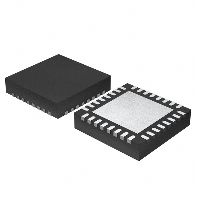
ICS810001I-21
32 Lead VFQFN
5mm x 5mm x 0.925mm package body
3.15mm x 3.15mm EPad Size
K Package
Top View
ICS810001DKI-21 REVISION A MARCH 21, 2013
2
©2013 Integrated Device Technology, Inc.
�ICS810001I-21 Data Sheet
FEMTOCLOCK® DUAL VCXO VIDEO PLL
Pin Descriptions and Characteristics
Table 1. Pin Descriptions
Number
Name
Type
Description
1, 2
LF1, LF0
Analog
Input/Output
Loop filter connection node pins.
3
ISET
Analog
Input/Output
Charge pump current setting pin.
4, 11, 25
VDD
Power
5,
22
nBP0,
nBP1
Input
6, 20, 29
GND
Power
7
CLK_SEL
Input
Pulldown
Input clock select. When HIGH selects CLK1. When LOW, selects CLK0.
LVCMOS / LVTTL interface levels.
8, 9
CLK1, CLK0
Input
Pulldown
Single-ended clock inputs. LVCMOS/LVTTL interface levels.
10, 14,
15, 16
V0, V1,
V2, V3
Input
Pulldown
VCXO PLL divider selection pins. LVCMOS/LVTTL interface levels.
12
MR
Input
Pulldown
Active HIGH Master Reset. When logic HIGH, the internal dividers are reset
causing the output to go low. When logic LOW, the internal dividers and the
output is enabled. LVCMOS/LVTTL interface levels.
13
MF
Input
Pulldown
FemtoClock multiplication factor select pin. LVCMOS/LVTTL interface
levels.
17
VDDA
Power
Analog supply pin.
18
VDDO
Power
Output supply pin.
19
Q
Output
Single-ended VCXO PLL clock output. LVCMOS/LVTTL interface levels.
21
OE
Input
Pullup
23, 24
N1, N0
Input
Pulldown
FemtoClock output divide select pins. LVCMOS/LVTTL interface levels.
26
XTAL_SEL
Input
Pulldown
Crystal select. When HIGH, selects XTAL1. When LOW, selects XTAL0.
LVCMOS/LVTTL interface levels.
27,
28
XTAL_OUT1,
XTAL_IN1
Input
Crystal oscillator interface. XTAL_IN1 is the input. XTAL_OUT1 is the
output.
30,
31
XTAL_OUT0,
XTAL_IN0
Input
Crystal oscillator interface. XTAL_IN0 is the input. XTAL_OUT0 is the
output.
32
VDDX
Power
Power supply pin for VCXO charge pump.
Core supply pins.
Pullup
PLL Bypass control pins. See block diagram.
Power supply ground.
Output enable. When logic LOW, the clock output is in high-impedance.
When logic HIGH, the output is enabled. LVCMOS/LVTTL interface levels.
NOTE: Pullup and Pulldown refer to internal input resistors. See Table 2, Pin Characteristics, for typical values.
Table 2. Pin Characteristics
Symbol
Parameter
CIN
Input Capacitance
CPD
Power Dissipation
Capacitance (per output)
Test Conditions
VDD = VDDX = VDDO = 3.465V
Minimum
Typical
Maximum
Units
4
pF
8.5
pF
RPULLUP
Input Pullup Resistor
51
k
RPULLDOWN
Input Pulldown Resistor
51
k
ROUT
Output Impedance
22.5
ICS810001DKI-21 REVISION A MARCH 21, 2013
3
©2013 Integrated Device Technology, Inc.
�ICS810001I-21 Data Sheet
FEMTOCLOCK® DUAL VCXO VIDEO PLL
Function Tables
Table 3A. VCXO PLL Pre- and Feedback Divider Function Table
Input
VCXO PLL Configuration
V3
V2
V1
V0
Pre-Divider P
Feedback- Divider M
0 (default)
0 (default)
0 (default)
0 (default)
1000
1000
0
0
0
1
1001
1000
0
0
1
0
11000
4004
0
0
1
1
11011
4000
0
1
0
0
11000
4000
0
1
0
1
4004
4004
0
1
1
0
4004
4000
0
1
1
1
1000
1001
1
0
0
0
250
91
1
0
0
1
253
92
1
0
1
0
92
92
1
0
1
1
1
600
1
1
0
0
1
800
1
1
0
1
1
1728
1
1
1
0
1
1716
1
1
1
1
1
960
ICS810001DKI-21 REVISION A MARCH 21, 2013
4
©2013 Integrated Device Technology, Inc.
�ICS810001I-21 Data Sheet
FEMTOCLOCK® DUAL VCXO VIDEO PLL
Table 3B. Input Frequency Table
Input
Crystal Frequency (fVCXO)
V3
V2
V1
V0
27MHz
26.973MHz
0 (default)
0 (default)
0 (default)
0 (default)
27.0000MHz
26.9730MHz
0
0
0
1
27.0270MHz
27.0000MHz
0
0
1
0
74.1758MHz
74.1016MHz
0
0
1
1
74.3243MHz
74.2499MHz
0
1
0
0
74.2500MHz
74.1758MHz
0
1
0
1
27.0000MHz
26.9730MHz
0
1
1
0
27.0270MHz
27.0000MHz
0
1
1
1
26.9730MHz
26.9461MHz
1
0
0
0
74.1758MHz
74.1016MHz
1
0
0
1
74.2500MHz
74.1758MHz
1
0
1
0
27.0000MHz
26.9730MHz
1
0
1
1
45.0000kHz
44.9550kHz
1
1
0
0
33.7500kHz
33.7163kHz
1
1
0
1
15.6250kHz
15.6094kHz
1
1
1
0
15.7343kHz
15.7185kHz
1
1
1
1
28.1250kHz
28.0969kHz
Table 3C. Output Frequency Table (dual PLL Mode)
FemtoClock Look-up Table
fVCXO
MF
N1
N0
Output Frequency fQ (MHz)
0
0
0
148.5000
0
0
1
74.2500
0
1
0
49.5000
0
1
1
33.0000
1
0
0
162.0000
1
0
1
81.0000
1
1
0
54.0000
1
1
1
36.0000
0
0
0
148.3515
0
0
1
74.1758
0
1
0
49.4505
0
1
1
32.9670
1
0
0
161.8380
1
0
1
80.9190
1
1
0
53.9460
1
1
1
35.9640
27MHz
26.973MHz
NOTE: Use the VCXO-PLL mode to achieve output Frequencies of 27MHz or 26.973MHz. See Table 3H.
ICS810001DKI-21 REVISION A MARCH 21, 2013
5
©2013 Integrated Device Technology, Inc.
�ICS810001I-21 Data Sheet
FEMTOCLOCK® DUAL VCXO VIDEO PLL
Table 3D. CLK_SEL Function Table
Input
CLK_SEL
Operation
0 (default)
Selects CLK0 as PLL reference input.
1
Selects CLK1 as PLL reference input.
Table 3E. MR Master Reset Function Table
Input
MR
0 (default)
1
Operation
Normal operation, internal dividers and the output Q are enabled.
Internal dividers are reset. Q output is in logic low state (with OE = 1).
Table 3F. FemtoCLock PLL Feedback Divider Function Table
Input
MF
Operation
0 (default)
Selects MF = 22. The 2nd stage PLL (FemtoClock. Multiplies the output frequency of the VCXO-PLL by 22).
1
Selects MF = 24. The 2nd stage PLL (FemtoClock. Multiplies the output frequency of the VCXO-PLL by 24).
Table 3G. PLL Output Divider Function Table
Input
N1
N0
Operation
0 (default)
0 (default)
Output divider N = 4.
0
1
Output divider N = 8.
1
0
Output divider N = 12.
1
1
Output divider N = 18.
Table 3H. PLL BYPASS Logic Function Table
Input
nBP1
nBP0
Operation
0
0
VCXO-PLL mode: The input reference frequency is divided by the pre-divider P and is multiplied by the
VCXO-PLL. fOUT = (fREF ÷ P) * M.
0
1
Test mode: The input reference frequency is divided by the pre-divider P and the output divider N and
bypasses both PLLs. fOUT = fREF ÷ (P * N).
1
0
FemtoClock Mode: The input reference frequency is divided by the pre-divider P multiplied by the 2nd
PLL (FemtoClock, MF). The 1st PLL (VCXO-PLL, M) is bypassed. This mode does not support jitter
attenuatiion. fOUT = (fREF ÷ P) * MF ÷ N.
1 (default)
1 (default)
Dual PLL Mode: both PLLs are cascaded for jitter attenuation and frequency multiplication.
fOUT = (fREF ÷ P) * M * MF ÷ N.
ICS810001DKI-21 REVISION A MARCH 21, 2013
6
©2013 Integrated Device Technology, Inc.
�ICS810001I-21 Data Sheet
FEMTOCLOCK® DUAL VCXO VIDEO PLL
Absolute Maximum Ratings
NOTE: Stresses beyond those listed under Absolute Maximum Ratings may cause permanent damage to the device. These ratings are stress
specifications only. Functional operation of product at these conditions or any conditions beyond those listed in the DC Characteristics or AC
Characteristics is not implied. Exposure to absolute maximum rating conditions for extended periods may affect product reliability.
Item
Rating
Supply Voltage, VDD
4.6V
Inputs, VI
XTAL_IN
Other Inputs
0V to VDD
-0.5V to VDD + 0.5V
Outputs, VO
-0.5V to VDDO + 0.5V
Package Thermal Impedance, JA
33.1C/W (0 mps)
Storage Temperature, TSTG
-65C to 150C
DC Electrical Characteristics
Table 4A. Power Supply DC Characteristics, VDD = VDDX = VDDO = 3.3V ± 5%, TA = -40°C to 85°C
Symbol
Parameter
Test Conditions
Minimum
Typical
Maximum
Units
VDD
Core Supply Voltage
3.135
3.3
3.465
V
VDDA
Analog Supply Voltage
VDD – 0.16
3.3
VDD
V
VDDO
Output Supply Voltage
3.135
3.3
3.465
V
VDDX
Charge Pump Supply Voltage
VDD – 0.04
3.3
3.465
V
IDD
Power Supply Current
294
mA
IDDA
Analog Supply Current
16
mA
IDDO
Output Supply Current
4
mA
IDDX
Charge Pump Supply Current
4
mA
Maximum
Units
No Load, OE = 0V
Table 4B. LVCMOS/LVTTL DC Characteristics, VDD = VDDX = VDDO = 3.3V ± 5%, TA = -40°C to 85°C
Symbol
Parameter
VIH
Input High Voltage
2.0
VDD + 0.3
V
VIL
Input Low Voltage
-0.3
0.8
V
IIH
Input
High
Current
IIL
Input
Low
Current
Test Conditions
Minimum
Typical
CLK[0:1],
CLK_SEL, XTAL_SEL,
V[3:0], N[1:0], MR, MF
VDD = VIN = 3.465V
150
µA
OE, nBP0, nBP1
VDD = VIN = 3.465V
5
µA
CLK[0:1],
CLK_SEL, XTAL_SEL,
V[3:0], N[1:0], MR, MF
VDD = 3.465V, VIN = 0V
-5
µA
OE, nBP0, nBP1
VDD = 3.465, VIN = 0V
-150
µA
2.6
V
VOH
Output High Voltage
IOH = -12mA
VOL
Output Low Voltage
IOL = 12mA
ICS810001DKI-21 REVISION A MARCH 21, 2013
7
0.5
V
©2013 Integrated Device Technology, Inc.
�ICS810001I-21 Data Sheet
FEMTOCLOCK® DUAL VCXO VIDEO PLL
AC Electrical Characteristics
Table 5. AC Characteristics, VDD = VDDX = VDDO = 3.3V ± 5%, TA = -40°C to 85°C
Symbol
Parameter
fOUT
Output Frequency
tjit(Ø)
RMS Phase Jitter, (Random);
NOTE 1
tR / tF
Output Rise/Fall Time
odc
Output Duty Cycle
tLOCK
VCXO & FemtoClock PLL Lock
Time; NOTE 2
Test Conditions
Minimum
nBP0, nBP1 = 00
Maximum
Units
14
35
MHz
nBP1 = 1
31
175
MHz
148.3516MHz,
Integration Range:
12kHz – 20MHz
20% to 80%
Typical
1.089
ps
250
750
ps
45
55
%
M = 92, Bandwidth = 475Hz
100
ms
M = 4004, Bandwidth = 6Hz
25
s
NOTE: Electrical parameters are guaranteed over the specified ambient operating temperature range, which is established when the device
is mounted in a test socket with maintained transverse airflow greater than 500 lfpm. The device will meet specifications after thermal
equilibrium has been reached under these conditions.
See Parameter Measurement Information Section.
NOTE 1: Refer to the Phase Noise Plot.
NOTE 2: Lock Time measured from power-up to stable output frequency.
ICS810001DKI-21 REVISION A MARCH 21, 2013
8
©2013 Integrated Device Technology, Inc.
�ICS810001I-21 Data Sheet
FEMTOCLOCK® DUAL VCXO VIDEO PLL
Typical Phase Noise at 148.3516MHz
Noise Power dBc
Hz
148.3516484MHz
RMS Phase Jitter (Random)
12kHz to 20MHz = 1.089ps (typical)
10Hz
100Hz
1kHz
10kHz
100kHz
1MHz
30MHZ
Offset Frequency (Hz)
ICS810001DKI-21 REVISION A MARCH 21, 2013
9
©2013 Integrated Device Technology, Inc.
�ICS810001I-21 Data Sheet
FEMTOCLOCK® DUAL VCXO VIDEO PLL
Parameter Measurement Information
1.65V±5%
1.65V±5%
VDD,
VDDO,
VDDX
80%
80%
Measurement Point
VDDA
LVCMOS
Q
20%
20%
tR
tF
GND
-1.65±5%
3.3V Output Load AC Test Circuit
Output Rise/Fall Time
Phase Noise Plot
V
Noise Power
DDO
2
Q
t PW
t
odc =
PERIOD
t PW
x 100%
Offset Frequency
f1
f2
RMS Phase Jitter =
1
* Area Under Curve Defined by the Offset Frequency Markers
2* *ƒ
t PERIOD
Output Duty Cycle/Pulse Width/Period
ICS810001DKI-21 REVISION A MARCH 21, 2013
Phase Jitter
10
©2013 Integrated Device Technology, Inc.
�ICS810001I-21 Data Sheet
FEMTOCLOCK® DUAL VCXO VIDEO PLL
Applications Information
Recommendations for Unused Input Pins
Inputs:
CLK Inputs
For applications not requiring the use of a clock input, it can be left
floating. Though not required, but for additional protection, a 1k
resistor can be tied from the CLK input to ground.
LVCMOS Control Pins
All control pins have internal pullup or pulldown resistors; additional
resistance is not required but can be added for additional protection.
A 1k resistor can be used.
VFQFN EPAD Thermal Release Path
In order to maximize both the removal of heat from the package and
the electrical performance, a land pattern must be incorporated on
the Printed Circuit Board (PCB) within the footprint of the package
corresponding to the exposed metal pad or exposed heat slug on the
package, as shown in Figure 1. The solderable area on the PCB, as
defined by the solder mask, should be at least the same size/shape
as the exposed pad/slug area on the package to maximize the
thermal/electrical performance. Sufficient clearance should be
designed on the PCB between the outer edges of the land pattern
and the inner edges of pad pattern for the leads to avoid any shorts.
and dependent upon the package power dissipation as well as
electrical conductivity requirements. Thus, thermal and electrical
analysis and/or testing are recommended to determine the minimum
number needed. Maximum thermal and electrical performance is
achieved when an array of vias is incorporated in the land pattern. It
is recommended to use as many vias connected to ground as
possible. It is also recommended that the via diameter should be 12
to 13mils (0.30 to 0.33mm) with 1oz copper via barrel plating. This is
desirable to avoid any solder wicking inside the via during the
soldering process which may result in voids in solder between the
exposed pad/slug and the thermal land. Precautions should be taken
to eliminate any solder voids between the exposed heat slug and the
land pattern. Note: These recommendations are to be used as a
guideline only. For further information, please refer to the Application
Note on the Surface Mount Assembly of Amkor’s Thermally/
Electrically Enhance Leadframe Base Package, Amkor Technology.
While the land pattern on the PCB provides a means of heat transfer
and electrical grounding from the package to the board through a
solder joint, thermal vias are necessary to effectively conduct from
the surface of the PCB to the ground plane(s). The land pattern must
be connected to ground through these vias. The vias act as “heat
pipes”. The number of vias (i.e. “heat pipes”) are application specific
PIN
PIN PAD
SOLDER
EXPOSED HEAT SLUG
GROUND PLANE
THERMAL VIA
SOLDER
LAND PATTERN
(GROUND PAD)
PIN
PIN PAD
Figure 1. P.C. Assembly for Exposed Pad Thermal Release Path – Side View (drawing not to scale)
ICS810001DKI-21 REVISION A MARCH 21, 2013
11
©2013 Integrated Device Technology, Inc.
�ICS810001I-21 Data Sheet
FEMTOCLOCK® DUAL VCXO VIDEO PLL
Schematic Example
Figure 2 (next page) shows an example ICS810001I-21application
schematic. This schematic example focuses on functional
connections and is not configuration specific. Refer to the pin
description and functional tables in the datasheet to ensure that the
logic control inputs are properly set.
As with any high speed analog circuitry, the power supply pins are
vulnerable to random noise. To achieve optimum jitter performance,
power supply isolation is required. The ICS810001I-21provides
separate power supply pins to isolate any high switching noise from
coupling into the internal PLL.
In this schematic, the device is operated at VDD = VDDA = VDDX=
VDDO =3.3V.
In order to achieve the best possible filtering, it is recommended that
the placement of the filter components be on the device side of the
PCB as close to the power pins as possible. If space is limited, the
0.1F capacitor in each power pin filter should be placed on the
device side. The other components can be on the opposite side of the
PCB.
Two 12pF parallel resonant crystals can used to facilitate clock
translations among common frequencies. Depending on the parasitic
capacity on the crystal terminals of the printed circuit board layout,
these values might require a slight adjustment to optimize the
frequency accuracy. Crystals with other load capacitance
specifications can be used. This will require adjusting the C1-C2 load
capacitor pair to tune each oscillator's center frequency. For this
device, the crystal load capacitors are required for proper operation.
See the IDT application note “Crystal - Tuning VCXO” for details.
Power supply filter recommendations are a general guideline to be
used for reducing external noise from coupling into the devices. The
filter performance is designed for a wide range of noise frequencies.
This low-pass filter starts to attenuate noise at approximately 10kHz.
If a specific frequency noise component is known, such as switching
power supplies frequencies, it is recommended that component
values be adjusted and if required, additional filtering be added.
Additionally, good general design practices for power plane voltage
stability suggests adding bulk capacitance in the local area of all
devices.
The ICS810001I-21 is packaged in a 32pin VFQFN package that
incorporates an ePAD thermal spreader. The ePAD is a backside
electrical contact of the package and is to be connected to the ground
directly under the package. See the data sheet section “VFQFN
EPAD Thermal Release Path” for details.
ICS810001DKI-21 REVISION A MARCH 21, 2013
12
©2013 Integrated Device Technology, Inc.
�ICS810001I-21 Data Sheet
FEMTOCLOCK® DUAL VCXO VIDEO PLL
Place each 0.1uF bypass cap directly adjacent to
its corresponding VDD, VDDA, VDDX or VDDO pin.
Logic Control Input Examples
VDD
Set Logic
Input to '1'
Set Logic
Input to '0'
VDD
2
VDD
3.3V
FB1
1
BLM18BB221SN1
RU1
1K
RU2
Not Install
To Logic
Input
pins
C8
0.1uF
C12
0.1uF
C6
10uF
To Logic
Input
pins
RD2
1K
MR
OE
12
21
nBP0
nBP1
5
22
V0
V1
V2
V3
10
14
15
16
N0
N1
24
23
XTAL_SEL
CLK_SEL
26
7
MF
13
R1
43
9
25
VDD
11
VDD
VDD
3.3V
C5
0.1uF
U1
4
RD1
Not Install
Ro
=7 Ohm
C11
0.1uF
MR
OE
VDDA
17
R5 10
VDDA
C9
0.1uF
nBP0
nBP1
V0
V1
V2
V3
VDDX
32
C7
10uF
R6 10
VDDX
C13
0.1uF
N0
N1
XTAL_SEL
CLK_SEL
VDDO
18
C10
10uF
3.3V
2
VDDO
FB2
1
BLM18BB221SN1
MF
C14
0.1uF
C16
10uF
C15
0.1uF
CLK0
Zo = 50 Ohm
LVCMOS Driv er
3.3V
Q
R2
43
8
Zo = 50
CLK1
Zo = 50 Ohm
LVCMOS Receiv er
LVCMOS Driv er
LF0
31
30
X1
27MHz (12pf )
LF0
R7
150k
XTAL_IN0
XTAL_OUT0
C18
1000pF
C19
0.22uF
X2
26.973MHz (12pf )
2
C4
TUNE
28
27
C1
TUNE
R3
33
Ro
=7 Ohm
C3
TUNE
19
LF1
XTAL_IN1
XTAL_OUT1
ISET
C2
TUNE
1
LF1
3
LF0
R24
TBD
R22
2.2k
C22
TBD
33
C1-C2 load cap pair and C3-C4 load cap
pair values set by the center frequency
tune procedure for Xtal0 and Xtal 1
oscillators respectivly.
6
20
29
GND
GND
GND
ePAD
C21
TBD
LF1
C20
TBD
R23 TBD
Three pole option for
reduced low frequency
jitter with larger
feedback dividers.
Consult IDT Applications
for filter values.
Figure 2. ICS810001I-21 Schematic Example
ICS810001DKI-21 REVISION A MARCH 21, 2013
13
©2013 Integrated Device Technology, Inc.
�ICS810001I-21 Data Sheet
FEMTOCLOCK® DUAL VCXO VIDEO PLL
VCXO-PLL EXTERNAL COMPONENTS
Choosing the correct external components and having a proper
printed circuit board (PCB) layout is a key task for quality operation
of the VCXO-PLL. In choosing a crystal, special precaution must be
taken with the package and load capacitance (CL). In addition,
frequency, accuracy and temperature range must also be
considered. Since the pulling range of a crystal also varies with the
package, it is recommended that a metal-canned package like HC49
be used. Generally, a metal-canned package has a larger pulling
range than a surface mounted device (SMD). For crystal selection
information, refer to the VCXO Crystal Selection Application Note.
The frequency of oscillation in the
LF0
LF1
third overtone mode is not
ISET
necessarily at exactly three times
RS RSET
the fundamental frequency. The
mechanical properties of the
CP CS
quartz element dictate the
position of the overtones relative
to the fundamental. The oscillator
XTAL_IN
circuit may excite both the
CTUNE
fundamental and overtone modes
simultaneously. This will cause a
XTAL_OUT
CTUNE
nonlinearity in the tuning curve.
This potential problem is why
VCXO crystals are required to be
tested for absence of any activity inside a ±200ppm window at three
times the fundamental frequency. Refer to FL_3OVT and
FL_3OVT_spurs in the crystal Characteristics table.
The crystal’s load capacitance CL characteristic determines its
resonating frequency and is closely related to the VCXO tuning
range. The total external capacitance seen by the crystal when
installed on a board is the sum of the stray board capacitance, IC
package lead capacitance, internal varactor capacitance and any
installed tuning capacitors (CTUNE).
If the crystal CL is greater than the total external capacitance, the
VCXO will oscillate at a higher frequency than the crystal
specification. If the crystal CL is lower than the total external
capacitance, the VCXO will oscillate at a lower frequency than the
crystal specification. In either case, the absolute tuning range is
reduced. The correct value of CL is dependent on the characteristics
of the VCXO. The recommended CL in the Crystal Parameter Table
balances the tuning range by centering the tuning curve.
The crystal and external loop filter components should be kept as
close as possible to the device. Loop filter and crystal traces should
be kept short and separated from each other. Other signal traces
should be kept separate and not run underneath the device, loop
filter or crystal components.
VCXO Characteristics Table
Symbol
Parameter
Typical
Units
kVCXO
VCXO Gain
6.6
kHz/V
CV_LOW
Low Varactor Capacitance
15
pF
CV_HIGH
High Varactor Capacitance
29
pF
VCXO-PLL Loop Bandwidth Selection Table
Bandwidth
Crystal Frequency (MHz)
M
RS (k)
CS (µF)
CP (µF)
RSET (k)
6Hz (Low)
27
4004
175
4.7
0.01
8.0
80Hz (Mid)
27
1000
150
0.22
0.001
2.21
475Hz (High)
27
92
125
0.1
0.0001
3.3
ICS810001DKI-21 REVISION A MARCH 21, 2013
14
©2013 Integrated Device Technology, Inc.
�ICS810001I-21 Data Sheet
FEMTOCLOCK® DUAL VCXO VIDEO PLL
Crystal Characteristics
Symbol
Parameter
Test Conditions
Minimum
Mode of Oscillation
Typical
Maximum
Units
Fundamental
27
MHz
26.973
MHz
fN
Frequency
fT
Frequency Tolerance
±20
ppm
fS
Frequency Stability
±20
ppm
Operating Temperature
Range
-40
85
0
C
CL
Load Capacitance
12
pF
CO
Shunt Capacitance
4
pF
CO / C1
Pullability Ratio
FL_3OVT
220
240
RD
Overtone FL
200
ppm
RD
Overtone FL Spurs
200
ppm
3
FL_3OVT_spurs
3
ESR
Equivalent Series Resistance
20
Drive Level
Aging @ 25 0C
ICS810001DKI-21 REVISION A MARCH 21, 2013
1
mW
First Year
±3
ppm
Ten Years
±10
ppm
15
©2013 Integrated Device Technology, Inc.
�ICS810001I-21 Data Sheet
FEMTOCLOCK® DUAL VCXO VIDEO PLL
Power Considerations
This section provides information on power dissipation and junction temperature for the ICS810001I-21.
Equations and example calculations are also provided.
1.
Power Dissipation.
The total power dissipation for the ICS810001I-21 is the sum of the core power plus the analog plus the power dissipation into the load.
The following is the power dissipation for VDD = 3.3V + 5% = 3.465V, which gives worst case results.
•
Power (core)MAX = 3.465 * (IDD + IDDA + IDDO + IDDX) = 3.465V * (294mA + 16mA + 4mA + 4mA) = 1101.87mW
•
Output Impedance ROUT Power Dissipation due to Loading 50 to VDD/2
Output Current IOUT = VDDO_MAX/[2 * (50 + ROUT)] = 3.465V/[2 * (50 +22.5)] = 23.9mA
•
Power Dissipation on the ROUT per LVCMOS output
Power (ROUT) = ROUT * (IOUT)2 = 22.5 * (23.9mA)2 = 12.9mW per output
•
Total Power (ROUT) = 12.9mW * 1 = 12.9mW
Dynamic Power Dissipation at 175MHz
Power (175MHz) = CPD * Frequency * (VDD)2 = 8.5pF * 175MHz * (3.465V)2 = 17.9mW per output
Total Power (175MHz) = 17.9mW * 1 = 17.9mW
Total Power Dissipation
•
Total Power
= Power (core)MAX + Power (ROUT) + Power (175MHz)
= 1101.87mW + 12.9mW + 17.9mW
= 1133mW
2. Junction Temperature.
Junction temperature, Tj, is the temperature at the junction of the bond wire and bond pad, and directly affects the reliability of the device. The
maximum recommended junction temperature is 125°C. Limiting the internal transistor junction temperature, Tj, to 125°C ensures that the bond
wire and bond pad temperature remains below 125°C.
The equation for Tj is as follows: Tj = JA * Pd_total + TA
Tj = Junction Temperature
JA = Junction-to-Ambient Thermal Resistance
Pd_total = Total Device Power Dissipation (example calculation is in section 1 above)
TA = Ambient Temperature
In order to calculate junction temperature, the appropriate junction-to-ambient thermal resistance JA must be used. Assuming no air flow and
a multi-layer board, the appropriate value is 33.1°C/W per Table 6 below.
Therefore, Tj for an ambient temperature of 85°C with all outputs switching is:
85°C + 1.133W * 33.1°C/W = 122.5°C. This is below the limit of 125°C.
This calculation is only an example. Tj will obviously vary depending on the number of loaded outputs, supply voltage, air flow and the type of
board (single layer or multi-layer).
Table 6. Thermal Resistance JA for 32 Lead VFQFN, Forced Convection
JA by Velocity
Meters per Second
Multi-Layer PCB, JEDEC Standard Test Boards
ICS810001DKI-21 REVISION A MARCH 21, 2013
0
1
3
33.1°C/W
28.1°C/W
25.4°C/W
16
©2013 Integrated Device Technology, Inc.
�ICS810001I-21 Data Sheet
FEMTOCLOCK® DUAL VCXO VIDEO PLL
Reliability Information
Table 7. JA vs. Air Flow Table for a 32 Lead VFQFN
JA vs. Air Flow
Meters per Second
Multi-Layer PCB, JEDEC Standard Test Boards
0
1
3
33.1°C/W
28.1°C/W
25.4°C/W
Transistor Count
The transistor count for ICS810001I-21 is: 9365
ICS810001DKI-21 REVISION A MARCH 21, 2013
17
©2013 Integrated Device Technology, Inc.
�ICS810001I-21 Data Sheet
FEMTOCLOCK® DUAL VCXO VIDEO PLL
Package Outline and Package Dimensions
Package Outline - K Suffix for 32 Lead VFQFN
(Ref.)
S eating Plan e
N &N
Even
(N -1)x e
(R ef.)
A1
Ind ex Area
L
A3
N
N
Anvil
Anvil
Singulation
Singula tion
e (Ty p.)
2 If N & N
1
are Even
2
OR
E2
(N -1)x e
(Re f.)
E2
2
To p View
b
A
(Ref.)
D
e
D2
2
N &N
Odd
0. 08
Chamfer 4x
0.6 x 0.6 max
OPTIONAL
C
D2
C
Bottom View w/Type A ID
Bottom View w/Type C ID
2
1
2
1
CHAMFER
4
Th er mal
Ba se
RADIUS
N N-1
4
N N-1
There are 2 methods of indicating pin 1 corner at the back of the VFQFN package:
1. Type A: Chamfer on the paddle (near pin 1)
2. Type C: Mouse bite on the paddle (near pin 1)
Table 8. Package Dimensions
Symbol
N
A
A1
A3
b
ND & NE
D&E
D2 & E2
e
L
JEDEC Variation: VHHD-2/-4
All Dimensions in Millimeters
Minimum
Nominal
32
0.80
0
0.25 Ref.
0.18
0.25
NOTE: The following package mechanical drawing is a generic
drawing that applies to any pin count VFQFN package. This drawing
is not intended to convey the actual pin count or pin layout of this
device. The pin count and pinout are shown on the front page. The
package dimensions are in Table 8.
Maximum
1.00
0.05
0.30
8
5.00 Basic
3.0
0.30
3.3
0.50 Basic
0.40
0.50
Reference Document: JEDEC Publication 95, MO-220
ICS810001DKI-21 REVISION A MARCH 21, 2013
18
©2013 Integrated Device Technology, Inc.
�ICS810001I-21 Data Sheet
FEMTOCLOCK® DUAL VCXO VIDEO PLL
Ordering Information
Table 9. Ordering Information
Part/Order Number
810001DKI-21LF
810001DKI-21LFT
Marking
ICS001DI21L
ICS001DI21L
ICS810001DKI-21 REVISION A MARCH 21, 2013
Package
“Lead-Free” 32 Lead VFQFN
“Lead-Free” 32 Lead VFQFN
19
Shipping Packaging
Tray
Tape & Reel
Temperature
-40°C to 85°C
-40°C to 85°C
©2013 Integrated Device Technology, Inc.
�ICS810001I-21 Data Sheet
FEMTOCLOCK® DUAL VCXO VIDEO PLL
We’ve Got Your Timing Solution
6024 Silver Creek Valley Road
San Jose, California 95138
Sales
800-345-7015 (inside USA)
+408-284-8200 (outside USA)
Fax: 408-284-2775
www.IDT.com/go/contact IDT
Technical Support Sales
netcom@idt.com
+480-763-2056
DISCLAIMER Integrated Device Technology, Inc. (IDT) and its subsidiaries reserve the right to modify the products and/or specifications described herein at any time and at IDT’s sole discretion. All information in this document,
including descriptions of product features and performance, is subject to change without notice. Performance specifications and the operating parameters of the described products are determined in the independent state and are not
guaranteed to perform the same way when installed in customer products. The information contained herein is provided without representation or warranty of any kind, whether express or implied, including, but not limited to, the
suitability of IDT’s products for any particular purpose, an implied warranty of merchantability, or non-infringement of the intellectual property rights of others. This document is presented only as a guide and does not convey any
license under intellectual property rights of IDT or any third parties.
IDT’s products are not intended for use in applications involving extreme environmental conditions or in life support systems or similar devices where the failure or malfunction of an IDT product can be reasonably expected to significantly affect the health or safety of users. Anyone using an IDT product in such a manner does so at their own risk, absent an express, written agreement by IDT.
Integrated Device Technology, IDT and the IDT logo are registered trademarks of IDT. Other trademarks and service marks used herein, including protected names, logos and designs, are the property of IDT or their respective third
party owners.
Copyright 2013. All rights reserved.
�