VCXO-To-6 LVCMOS Outputs
81006
OBSOLETE
DATA SHEET
General Description
Features
The 81006 is a high performance, low jitter/ low phase noise VCXO.
The 81006 works in conjunction with a pullable crystal to generate an
output clock over the range of 12MHz – 31.25MHz and has 6
LVCMOS outputs, effectively integrating a fanout buffer function.
• Six LVCMOS/LVTTL outputs, 20 nominal output impedance
• Output Q5 can be selected for ÷1 or ÷2 frequency relative to the
crystal frequency
• Output frequency range: 12MHz to 31.25MHz
The frequency of the VCXO is adjusted by the VC control voltage
input. The output range is ±100ppm around the nominal crystal
frequency. The VC control voltage range is 0 – VDD. The device is
packaged in a small 4mm x 4mm VFQFN package and is ideal for use
on space constrained boards typically encountered in ADSL/VDSL
applications.
• Crystal pull range: ±90ppm (typical)
• Synchronous output enable places outputs in High-
Impedance state
• On-chip filter on VIN to suppress noise modulation of VCXO
• VDD/VDDO combinations
3.3V/3.3V
3.3V/2.5V
3.3V/1.8V
2.5V/2.5V
2.5V/1.8V
• 4mm x 4mm 20-Lead VFQFN package is ideal for space
constrained designs
• 0°C to 70°C ambient operating temperature
• Lead-free (RoHS 6) packaging
VCXO
Q2
XTAL_OUT
0: ÷1
1: ÷2
DIV_SEL_Q5
OE1
Q1
VDDO
Q0
20 19 18 17 16
15
XTAL_OUT
2
14
Q2
VDD
3
13
VDDO
VC
4
12
Q3
DIV_SEL_Q5
5
6
7
8
9
11
10
Q4
XTAL_IN
1
Q5
Q1
XTAL_IN
VDDO
Q0
LP Filter
GND
SYNC
OE1
VC
Pullup
GND
OE0
Pin Assignment
OE0
Block Diagram
GND
GND
Q3
81006
Q4
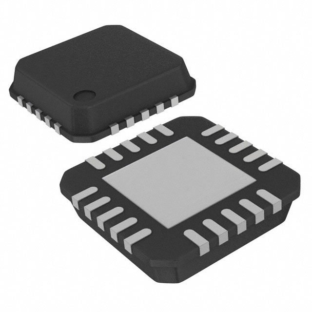
20-Lead VFQFN
4mm x 4mm x 0.925 package body
K Package
Top View
Q5
Pulldown
Pullup
SYNC
81006 REVISION B 7/29/16
1
©2016 Integrated Device Technology, Inc.
�81006 DATA SHEET
Pin Descriptions and Characteristics
Table 1. Pin Descriptions1
Number
Name
Type
Description
1, 2
XTAL_IN,
XTAL_OUT
Input
3
VDD
Power
4
VC
Input
5
DIV_SEL_Q5
Input
Pulldown
Output divider select pin for Q5 output. When LOW, ÷1. When HIGH, ÷2.
LVCMOS/LVTTL interface levels.
6
OE1
Input
Pullup
Output enable pin. When HIGH, Q5 output is enabled. When LOW, forces
Q5 to a high impedance state. LVCMOS/LVTTL interface levels.
7, 11, 15, 19
GND
Power
Power supply ground.
8, 10, 12, 14,
16, 18
Q5, Q4, Q3,
Q2, Q1, Q0
Output
Single-ended clock outputs. LVCMOS/LVTTL interface levels. 20output
impedance.
9, 13, 17
VDDO
Power
Output supply pins.
20
OE0
Input
Crystal oscillator interface. XTAL_IN is the input. XTAL_OUT is the output.
Positive supply pin.
Control voltage input.
Pullup
Output enable pin. When HIGH, Q0:Q4 outputs are enabled. When LOW,
forces Q0:Q4 to a high impedance state. LVCMOS/LVTTL interface levels.
NOTE 1: Pullup and Pulldown refer to internal input resistors. See Table 2, Pin Characteristics, for typical values.
Table 2. Pin Characteristics
Symbol
Parameter
CIN
Input
Capacitance
Test Conditions
OE0, OE1
Minimum
Typical
4
VDD = VDDO = 3.465V
CPD
Power Dissipation
Capacitance
Maximum
VDD = 3.465V or 2.625V,
VDDO = 2.625V
VDD = 3.465V or 2.625V,
VDDO = 2V
Units
pF
3
pF
4
pF
6
pF
RPULLUP
Input Pullup Resistor
51
k
RPULLDOWN
Input Pulldown Resistor
51
k
ROUT
Output Impedance
VCXO-TO-6 LVCMOS OUTPUTS
VDDO = 3.3V
20
VDDO = 2.5V
25
VDDO = 1.8V
38
2
REVISION B 7/29/16
�81006 DATA SHEET
Absolute Maximum Ratings
NOTE: Stresses beyond those listed under Absolute Maximum Ratings may cause permanent damage to the device. These ratings are stress
specifications only. Functional operation of product at these conditions or any conditions beyond those listed in the DC Electrical Characteristics
or AC Characteristics is not implied. Exposure to absolute maximum rating conditions for extended periods may affect product reliability.
Item
Rating
Supply Voltage, VDD
4.6V
Inputs, VI
-0.5V to VDD + 0.5V
Outputs, VO
-0.5V to VDDO + 0.5V
Package Thermal Impedance, JA
60.4°C/W (0 mps)
Storage Temperature, TSTG
-65C to 150C
DC Electrical Characteristics
Table 3A. Power Supply DC Characteristics, VDD = 3.3V ±5%, VDDO = 3.3V ±5%, 2.5V ±5% or 1.8V ±0.2V, TA = 0°C to 70°C
Symbol
Parameter
VDD
Positive Supply Voltage
VDDO
Test Conditions
Output Supply Voltage
Minimum
Typical
Maximum
Units
3.135
3.3
3.465
V
3.135
3.3
3.465
V
2.375
2.5
2.625
V
1.6
1.8
2.0
V
IDD
Power Supply Current
50
mA
IDDO
Output Supply Current
20
mA
Table 3B. Power Supply DC Characteristics, VDD = 2.5V ±5%, VDDO = 2.5V ±5% or 1.8V ±0.2V, TA = 0°C to 70°C
Symbol
Parameter
VDD
Positive Supply Voltage
VDDO
Output Supply Voltage
IDD
IDDO
Minimum
Typical
Maximum
Units
2.375
2.5
2.625
V
2.375
2.5
2.625
V
1.6
1.8
2.0
V
Power Supply Current
50
mA
Output Supply Current
20
mA
REVISION B 7/29/16
Test Conditions
3
VCXO-TO-6 LVCMOS OUTPUTS
�81006 DATA SHEET
Table 3C. LVCMOS/LVTTL DC Characteristics, TA = 0°C to 70°C
Symbol
Parameter
VIH
Input High Voltage
VIL
Input Low
Voltage
VC
VCXO Control Voltage
IIH
Input
High Current
IIL
Input
Low Current
II
Input Current of VC pin
VOH
VOL
Output High
OE0, OE1,
DIV_SEL_Q5
Test Conditions
Minimum
VDD = 3.3V ±5%
Typical
Maximum
Units
2
VDD + 0.3
V
VDD = 2.5V ±5%
1.7
VDD + 0.3
V
VDD = 3.3V ±5%
-0.3
0.8
V
VDD = 2.5V ±5%
-0.3
0.7
V
0
VDD
V
DIV_SEL_Q5
VDD = 3.3V or 2.5V ±5%
150
µA
OE0, OE1
VDD = 3.3V or 2.5V ±5%
5
µA
DIV_SEL_Q5
VDD = 3.3V or 2.5V ±5%
-5
µA
OE0, OE1
VDD = 3.3V or 2.5V ±5%
-150
µA
VDD = 3.465V or 2.625V
-100
VDDO = 3.3V ±5%
2.6
V
VDDO = 2.5V ±5%
1.8
V
VDDO = 1.8V ±0.2V
1.5
V
Voltage1
Output Low Voltage1
100
µA
VDDO = 3.3V or 2.5V ±5%
0.5
V
VDDO = 1.8V ±0.2V
0.4
V
NOTE 1: Outputs terminated with 50to VDDO/2. See Parameter Measurement Information section, “Load Test Circuit” diagrams.
VCXO-TO-6 LVCMOS OUTPUTS
4
REVISION B 7/29/16
�81006 DATA SHEET
AC Characteristics
Table 4A. AC Characteristics, VDD = VDDO = 3.3V ±5%, TA = 0°C to 70°C
Symbol
Parameter
fOUT
Output Frequency
Test Conditions
1
tjit(Ø)
RMS Phase Jitter (Random)
tsk(o)
Output Skew2, 3
tR / tF
Output Rise/Fall Time
odc
Output Duty Cycle
Minimum
Typical
Maximum
Units
12
19.44
31.25
MHz
Integration Range: 1kHz – 1MHz
0.35
Q0:Q4
Q0:Q5
30
ps
100
ps
200
700
ps
44
56
%
DIV_SEL_Q5 = ÷1
20% to 80%
ps
NOTE 1: Refer to the Phase Noise Plot.
NOTE 2: Defined as skew between outputs at the same supply voltage and with equal load conditions. Measured at the output differential
crosspoints.
NOTE 3: This parameter is defined in accordance with JEDEC Standard 65.
Table 4B. AC Characteristics, VDD = 3.3V ±5%, VDDO = 2.5V ±5%, TA = 0°C to 70°C
Symbol
Parameter
fOUT
Output Frequency
Test Conditions
(Random)1
tjit(Ø)
RMS Phase Jitter
tsk(o)
Output Skew2, 3
tR / tF
Output Rise/Fall Time
odc
Output Duty Cycle
Minimum
Typical
Maximum
Units
12
19.44
31.25
MHz
Integration Range: 1kHz – 1MHz
0.38
Q0:Q4
Q0:Q5
20
ps
90
ps
300
800
ps
45
55
%
DIV_SEL_Q5 = ÷1
20% to 80%
ps
NOTE 1: Refer to the Phase Noise Plot.
NOTE 2: Defined as skew between outputs at the same supply voltage and with equal load conditions. Measured at the output differential
crosspoints.
NOTE 3: This parameter is defined in accordance with JEDEC Standard 65.
Table 4C. AC Characteristics, VDD = 3.3V ±5%, VDDO = 1.8V ±0.2V, TA = 0°C to 70°C
Symbol
Parameter
fOUT
Output Frequency
Test Conditions
(Random)1
tjit(Ø)
RMS Phase Jitter
tsk(o)
Output Skew2, 3
tR / t F
Output Rise/Fall Time
odc
Output Duty Cycle
Minimum
Typical
Maximum
Units
12
19.44
31.25
MHz
Integration Range: 1kHz – 1MHz
0.27
Q0:Q4
Q0:Q5
46
ps
175
ps
450
1400
ps
44
56
%
DIV_SEL_Q5 = ÷1
20% to 80%
ps
NOTE 1: Refer to the Phase Noise Plot.
NOTE 2: Defined as skew between outputs at the same supply voltage and with equal load conditions. Measured at the output differential
crosspoints.
NOTE 3: This parameter is defined in accordance with JEDEC Standard 65.
REVISION B 7/29/16
5
VCXO-TO-6 LVCMOS OUTPUTS
�81006 DATA SHEET
Table 4D. AC Characteristics, VDD = VDDO = 2.5V ±5%, TA = 0°C to 70°C
Symbol
Parameter
fOUT
Output Frequency
Test Conditions
1
tjit(Ø)
RMS Phase Jitter (Random)
tsk(o)
Output Skew2, 3
tR / t F
Output Rise/Fall Time
odc
Output Duty Cycle
Minimum
Typical
Maximum
Units
12
19.44
31.25
MHz
Integration Range: 1kHz – 1MHz
0.28
Q0:Q4
Q0:Q5
25
ps
100
ps
300
800
ps
45
55
%
DIV_SEL_Q5 = ÷1
20% to 80%
ps
NOTE 1: Refer to the Phase Noise Plot.
NOTE 2: Defined as skew between outputs at the same supply voltage and with equal load conditions. Measured at the output differential
crosspoints.
NOTE 3: This parameter is defined in accordance with JEDEC Standard 65.
Table 4E. AC Characteristics, VDD = 2.5V ±5%, VDDO = 1.8V ±0.2V, TA = 0°C to 70°C
Symbol
Parameter
fOUT
Output Frequency
Test Conditions
(Random)1
tjit(Ø)
RMS Phase Jitter
tsk(o)
Output Skew2, 3
tR / t F
Output Rise/Fall Time
odc
Output Duty Cycle
Minimum
Typical
Maximum
Units
12
19.44
31.25
MHz
Integration Range: 1kHz – 1MHz
0.26
Q0:Q4
Q0:Q5
40
ps
175
ps
450
1400
ps
40
60
%
DIV_SEL_Q5 = ÷1
20% to 80%
ps
NOTE 1: Refer to the Phase Noise Plot.
NOTE 2: Defined as skew between outputs at the same supply voltage and with equal load conditions. Measured at the output differential
crosspoints.
NOTE 3: This parameter is defined in accordance with JEDEC Standard 65.
VCXO-TO-6 LVCMOS OUTPUTS
6
REVISION B 7/29/16
�81006 DATA SHEET
Typical Phase Noise at 19.44MHz @3.3V CORE/3.3V Output
0
-10
-20
-30
19.44MHz
-40
RMS Phase Jitter (Random)
1kHz to 1MHz = 0.35ps (typical)
Noise Power (dBc / Hz)
-50
-60
-70
-80
-90
-100
-110
-120
-130
-140
-150
-160
-170
-180
-190
100
1k
10k
100k
1M
Offset Frequency (Hz)
REVISION B 7/29/16
7
VCXO-TO-6 LVCMOS OUTPUTS
�81006 DATA SHEET
Parameter Measurement Information
1.65V±5%
2.05V±5%
1.25V±5%
SCOPE
VDD
VDDO
SCOPE
VDD
Qx
VDDO
Qx
GND
GND
-1.65V±5%
-1.25V±5%
3.3V Core/3.3V Output Load Test Circuit
3.3V Core/2.5V Output Load Test Circuit
2.4V±0.065V
1.25V±5%
0.9V±0.1V
SCOPE
VDD
VDDO
SCOPE
VDD
VDDO
Qx
Qx
GND
GND
-1.25V±5%
-0.9V±0.1V
3.3V Core/1.8V Output Load Test Circuit
2.5V Core/2.5V Output Load Test Circuit
1.6V±0.025V
0.9V±0.1V
SCOPE
VDD
VDDO
Qx
GND
-0.9V±0.1V
2.5V Core/1.8V Output Load Test Circuit
VCXO-TO-6 LVCMOS OUTPUTS
RMS Phase Jitter
8
REVISION B 7/29/16
�81006 DATA SHEET
Parameter Measurement Information, Continued
V
DDO
Q0:Q5
2
Qx
V
DDO
Qy
2
tsk(o)
Output Skew
Output Duty Cycle/Pulse Width/Period
80%
80%
20%
20%
Q0:Q5
tR
tF
Output Rise/Fall Time
REVISION B 7/29/16
9
VCXO-TO-6 LVCMOS OUTPUTS
�81006 DATA SHEET
Applications Information
VCXO Crystal Selection
Choosing a crystal with the correct characteristics is one of the most
critical steps in using a Voltage Controlled Crystal Oscillator (VCXO).
The crystal parameters affect the tuning range and accuracy of a
VC
“Control Voltage”
VCXO. Below are the key variables and an example of using the
crystal parameters to calculate the tuning range of the VCXO.
Oscillator
CV
CV
VCXO (Internal)
XTAL
CS1
CS2
CL1
CL2
Optional
Figure 1. VCXO Oscillator Circuit
VC
-Control voltage used to tune frequency
CV
-Varactor capacitance, varies due to the change in control voltage
CL1
CL2
-Load tuning capacitance used for fine tuning or centering nominal frequency
CS1
CS2
-Stray Capacitance caused by pads, vias, and other board parasitics
Table 5. Example Crystal Parameters
Symbol
Parameter
Test Conditions
Min
Typical
Max
fN
Nominal Frequency
fT
Frequency Tolerance
±20
ppm
fS
Frequency Stability
±20
ppm
70
°C
19.44
Operating Temp Range
0
Units
MHz
CL
Load Capacitance
12
pF
CO
Shunt Capacitance
4
pF
CO/C1
Pullability Ratio
ESR
Equivalent Series Resistance
20
Drive Level
1
220
Aging @ 25°C
±3 per year
Mode of Operation
VCXO-TO-6 LVCMOS OUTPUTS
240
mW
ppm
Fundamental
10
REVISION B 7/29/16
�81006 DATA SHEET
Table 6. Varactor Parameters
Symbol
Parameter
CV_LOW
Low Varactor Capacitance
VC = 0V
15.4
pF
CV_HIGH
High Varactor Capacitance
VC = 3.3V
29.6
pF
Test Condition
Minimum
Typical
Maximum
Unit
Formulas
C Low
C
C
L1
C S 1 CV _ Low C L 2 C S 2 CV _ Low
C High
L1 C S 1 CV _ Low C L 2 C S 2 CV _ Low
C
C
L1
C S 1 CV _ High C L 2 C S 2 CV _ High
L1 C S 1 CV _ High C L 2 C S 2 CV _ High
• CLow is the effective capacitance due to the low varactor capacitance, load capacitance and stray capacitance.
CLow determines the high frequency component on the TPR.
• CHigh is the effective capacitance due to the high varactor capacitance, load capacitance and stray capacitance.
CHigh determines the low frequency component on the TPR.
1
1
10 6
Total Pull Range (TPR )
C
C
2 C 0 C 1 1 Low C 0 2 C 0 C 1 1 High C 0
Absolute Pull Range (APR) = Total Pull Range – (Frequency Tolerance + Frequency Stability + Aging)
Example Calculations
Third, though many boards will not require load tuning capacitors
(CL1, CL2), it is recommended for long-term consistent performance
of the system that two tuning capacitor pads be placed into every
design. Typical values for the load tuning capacitors will range from 0
to 4 pF.
Using the tables and figures above, we can now calculate the TPR
and APR of the VCXO using the example crystal parameters. For the
numerical example below there were some assumptions made. First,
the stray capacitance (CS1, CS2), which is all the excess capacitance
due to board parasitic, is 4pF. Second, the expected lifetime of the
project is 5 years; hence the inaccuracy due to aging is ±15ppm.
C Low
0 4 pf 15.4 pf 0 4 pf 15.4 pf 9.7 pf
0 4 pf 15.4 pf 0 4 pf 15.4 pf
C High
0 4 pf 29.6 pf 0 4 pf 29.6 pf 16.8 pf
0 4 pf 29.6 pf 0 4 pf 29.6 pf
1
1
10 6 226 .5 ppm
TPR
2 220 1 16.8 pF
2 220 1 9.7 pF
4 pF
4 pF
TPR = ±113.25ppm
APR = 113.25ppm – (20ppm + 20ppm + 15ppm) = ±58.25ppm
Also, with the equations above, one can vary the frequency tolerance,
temperature stability, and aging or shunt capacitance to achieve the
required pullability.
The example above will ensure a total pull range of ±113.25 ppm with
an APR of ±58.25ppm. Many times, board designers may select their
own crystal based on their application. If the application requires a
tighter APR, a crystal with better pullability (C0/C1 ratio) can be used.
REVISION B 7/29/16
11
VCXO-TO-6 LVCMOS OUTPUTS
�81006 DATA SHEET
Recommendations for Unused Input Pins
Inputs:
Outputs:
Control Pins
LVCMOS Outputs
All control pins have internal pull-ups or pull-downs; additional
resistance is not required but can be added for additional protection.
A 1kresistor can be used. The VC pin can not be floated.
All unused LVCMOS output can be left floating. We recommend
that there is no trace attached.
Schematic Example
example is shown in the schematic. Additional termination
approaches are shown in the LVCMOS Termination Application Note.
Figure 2 shows an example of 81006 application schematic. The
decoupling capacitors should be located as close as possible to the
power pin. For the LVCMOS 20 output drivers, series termination
Pull-up VDD
example
R4
1K
VDD
R1
Zo = 50
U1
OE0
GND
Q0
VDDO
Q1
C1
SPARE
1
2
3
4
5
XTAL
XTAL_IN
XTAL_OUT
VDD
VC
DIV_SEL_Q5
15
14
13
12
11
GND
Q2
VDDO
Q3
GND
OE1
GND
Q5
VDDO
Q4
C2
SPARE
81006
Pull-down
example
6
7
8
9
10
VC
VC = 0V to VDD
30
20
19
18
17
16
Quartz crystal should be
placed as close to the
device as possible.
VDDO
R3
1K
R2
Zo = 50
VDD
30
R5
(U1-3)
(U1-9)
(U1-13)
(U1-17)
VDDO
VDD
C7
10uf
1K
C6
0.1uF
C5
0.1uF
C4
0.1uF
Unused outputs can be left floating. There should be
no trace attached to unused outputs. Device
characterized and specification limits set with all
outputs terminated.
C3
0.1uF
Figure 2. 81006 Schematic Example
VCXO-TO-6 LVCMOS OUTPUTS
12
REVISION B 7/29/16
�81006 DATA SHEET
VFQFN EPAD Thermal Release Path
In order to maximize both the removal of heat from the package and
the electrical performance, a land pattern must be incorporated on
the Printed Circuit Board (PCB) within the footprint of the package
corresponding to the exposed metal pad or exposed heat slug on the
package, as shown in Figure 3. The solderable area on the PCB, as
defined by the solder mask, should be at least the same size/shape
as the exposed pad/slug area on the package to maximize the
thermal/electrical performance. Sufficient clearance should be
designed on the PCB between the outer edges of the land pattern
and the inner edges of pad pattern for the leads to avoid any shorts.
and dependent upon the package power dissipation as well as
electrical conductivity requirements. Thus, thermal and electrical
analysis and/or testing are recommended to determine the minimum
number needed. Maximum thermal and electrical performance is
achieved when an array of vias is incorporated in the land pattern. It
is recommended to use as many vias connected to ground as
possible. It is also recommended that the via diameter should be 12
to 13mils (0.30 to 0.33mm) with 1oz copper via barrel plating. This is
desirable to avoid any solder wicking inside the via during the
soldering process which may result in voids in solder between the
exposed pad/slug and the thermal land. Precautions should be taken
to eliminate any solder voids between the exposed heat slug and the
land pattern. Note: These recommendations are to be used as a
guideline only. For further information, please refer to the Application
Note on the Surface Mount Assembly of Amkor’s Thermally/
Electrically Enhance Leadframe Base Package, Amkor Technology.
While the land pattern on the PCB provides a means of heat transfer
and electrical grounding from the package to the board through a
solder joint, thermal vias are necessary to effectively conduct from
the surface of the PCB to the ground plane(s). The land pattern must
be connected to ground through these vias. The vias act as “heat
pipes”. The number of vias (i.e. “heat pipes”) are application specific
PIN
PIN PAD
SOLDER
EXPOSED HEAT SLUG
GROUND PLANE
THERMAL VIA
SOLDER
LAND PATTERN
(GROUND PAD)
PIN
PIN PAD
Figure 3. P.C. Assembly for Exposed Pad Thermal Release Path – Side View (drawing not to scale)
REVISION B 7/29/16
13
VCXO-TO-6 LVCMOS OUTPUTS
�81006 DATA SHEET
Reliability Information
Table 7. JA vs. Air Flow Table for a 20-Lead VFQFN
JA vs. Air Flow
Meters per Second
Multi-Layer PCB, JEDEC Standard Test Boards
0
1
3
60.4°C/W
52.8°C/W
46.0°C/W
Transistor Count
The transistor count for the IS81006 is: 983
VCXO-TO-6 LVCMOS OUTPUTS
14
REVISION B 7/29/16
�81006 DATA SHEET
Package Outline and Package Dimensions
Package Outline - K Suffix for 20-Lead VFQFN
Table 8. Package Dimensions for 20-Lead VFQFN
NOTE:
JEDEC Variation:
All Dimensions in Millimeters
The drawing and dimension data originate from IDT package
outline drawing PSC-4170, rev03.
Symbol
Minimum
Nom
Maximum
b
0.20
0.25
0.30
1. Dimensions and tolerances conform to ASME Y14.5M-1994
D
3.90
4.00
4.10
2. All dimensions are in millimeters. All angles are in degrees.
E
3.90
4.00
4.10
3. N is the total number of terminals.
D2
1.95
2.10
2.25
4. All specifications comply with JEDEC MO-220.
E2
1.95
2.10
2.25
L
0.45
0.55
0.65
e
0.50 BSC
N
20
A
0.80
A1
0.00
A3
0.90
1.00
0.02
0.05
0.2 REF
Reference Document: JEDEC Publication 95, MO-220
REVISION B 7/29/16
15
VCXO-TO-6 LVCMOS OUTPUTS
�81006 DATA SHEET
Ordering Information
Table 9. Ordering Information
Part/Order Number
Marking
Package
Shipping Packaging
Temperature
81006AKLF
1006AL
“Lead-Free” 20-Lead VFQFN
Tube
0°C to 70°C
81006AKLFT
1006AL
“Lead-Free” 20-Lead VFQFN
Tape & Reel
0°C to 70°C
VCXO-TO-6 LVCMOS OUTPUTS
16
REVISION B 7/29/16
�81006 DATA SHEET
Revision History Sheet
Rev
Table
Page
1
B
T4A - T4D
T9
4-5
15
T8
T9
15
15
1, 16
B
B
B
REVISION B 7/29/16
1
Description of Change
Date
General Description and Features section changed output frequency max. from
40MHz to 31.25MHz.
AC Tables - changed output frequency from 40MHz max. to 31.25MHz max.
Ordering Information Table - added lead-free marking
10/8/08
Updated datasheet to current format.
Updated Package Outline
Updated Package Dimensions to reflect tighter tolerances.
Removed leaded ordering option.
7/23/14
PDN - CQ-15-01
2/10/15
Removed ICS from part number.
Added OBSOLETE to the data sheet front page.
7/29/16
17
VCXO-TO-6 LVCMOS OUTPUTS
�Corporate Headquarters
Sales
Tech Support
6024 Silver Creek Valley Road
San Jose, CA 95138 USA
1-800-345-7015 or 408-284-8200
Fax: 408-284-2775
www.IDT.com
email: clocks@idt.com
DISCLAIMER Integrated Device Technology, Inc. (IDT) and its subsidiaries reserve the right to modify the products and/or specifications described herein at any time and at IDT’s sole discretion. All information in
this document, including descriptions of product features and performance, is subject to change without notice. Performance specifications and the operating parameters of the described products are determined
in the independent state and are not guaranteed to perform the same way when installed in customer products. The information contained herein is provided without representation or warranty of any kind, whether
express or implied, including, but not limited to, the suitability of IDT’s products for any particular purpose, an implied warranty of merchantability, or non-infringement of the intellectual property rights of others. This
document is presented only as a guide and does not convey any license under intellectual property rights of IDT or any third parties.
IDT’s products are not intended for use in applications involving extreme environmental conditions or in life support systems or similar devices where the failure or malfunction of an IDT product can be reasonably
expected to significantly affect the health or safety of users. Anyone using an IDT product in such a manner does so at their own risk, absent an express, written agreement by IDT.
While the information presented herein has been checked for both accuracy and reliability, Integrated Device Technology (IDT) assumes no responsibility for either its use or for the infringement of any patents or
other rights of third parties, which would result from its use. No other circuits, patents, or licenses are implied. This product is intended for use in normal commercial applications. Any other applications, such as
those requiring extended temperature ranges, high reliability or other extraordinary environmental requirements are not recommended without additional processing by IDT. IDT reserves the right to change any
circuitry or specifications without notice. IDT does not authorize or warrant any IDT product for use in life support devices or critical medical instruments.
Integrated Device Technology, IDT and the IDT logo are registered trademarks of IDT. Product specification subject to change without notice. Other trademarks and service marks used herein, including protected
names, logos and designs, are the property of IDT or their respective third party owners.
Copyright ©2016 Integrated Device Technology, Inc.. All rights reserved.
�IMPORTANT NOTICE AND DISCLAIMER
RENESAS ELECTRONICS CORPORATION AND ITS SUBSIDIARIES (“RENESAS”) PROVIDES TECHNICAL
SPECIFICATIONS AND RELIABILITY DATA (INCLUDING DATASHEETS), DESIGN RESOURCES (INCLUDING
REFERENCE DESIGNS), APPLICATION OR OTHER DESIGN ADVICE, WEB TOOLS, SAFETY INFORMATION, AND
OTHER RESOURCES “AS IS” AND WITH ALL FAULTS, AND DISCLAIMS ALL WARRANTIES, EXPRESS OR IMPLIED,
INCLUDING, WITHOUT LIMITATION, ANY IMPLIED WARRANTIES OF MERCHANTABILITY, FITNESS FOR A
PARTICULAR PURPOSE, OR NON-INFRINGEMENT OF THIRD PARTY INTELLECTUAL PROPERTY RIGHTS.
These resources are intended for developers skilled in the art designing with Renesas products. You are solely responsible
for (1) selecting the appropriate products for your application, (2) designing, validating, and testing your application, and (3)
ensuring your application meets applicable standards, and any other safety, security, or other requirements. These
resources are subject to change without notice. Renesas grants you permission to use these resources only for
development of an application that uses Renesas products. Other reproduction or use of these resources is strictly
prohibited. No license is granted to any other Renesas intellectual property or to any third party intellectual property.
Renesas disclaims responsibility for, and you will fully indemnify Renesas and its representatives against, any claims,
damages, costs, losses, or liabilities arising out of your use of these resources. Renesas' products are provided only subject
to Renesas' Terms and Conditions of Sale or other applicable terms agreed to in writing. No use of any Renesas resources
expands or otherwise alters any applicable warranties or warranty disclaimers for these products.
(Rev.1.0 Mar 2020)
Corporate Headquarters
Contact Information
TOYOSU FORESIA, 3-2-24 Toyosu,
Koto-ku, Tokyo 135-0061, Japan
www.renesas.com
For further information on a product, technology, the most
up-to-date version of a document, or your nearest sales
office, please visit:
www.renesas.com/contact/
Trademarks
Renesas and the Renesas logo are trademarks of Renesas
Electronics Corporation. All trademarks and registered
trademarks are the property of their respective owners.
© 2020 Renesas Electronics Corporation. All rights reserved.
�


 工商网监
湘ICP备2023018690号
工商网监
湘ICP备2023018690号
