Jitter Attenuator & FemtoClock NG®
Multiplier
813N252DI-02
DATA SHEET
General Description
Features
The 813N252DI-02 device uses IDT's fourth generation
FemtoClock® NG technology for optimal high clock frequency and
low phase noise performance, combined with a low power
consumption and high power supply noise rejection. The
813N252DI-02 is a PLL based synchronous multiplier that is
optimized for PDH or SONET to Ethernet clock jitter attenuation and
frequency translation.
•
•
•
Fourth generation FemtoClock® NG technology
•
Two differential inputs support the following input types: LVPECL,
LVDS, LVHSTL, HCSL
•
Accepts input frequencies from 8kHz to 155.52MHz including
8kHz, 1.544MHz, 2.048MHz, 19.44MHz, 25MHz, 77.76MHz,
125MHz and 155.52MHz
•
Crystal interface optimized for a 27MHz, 10pF parallel resonant
crystal
•
Attenuates the phase jitter of the input clock by using a low-cost
fundamental mode crystal
•
Customized settings for jitter attenuation and reference tracking
using an external loop filter connection
•
FemtoClock NG frequency multiplier provides low jitter, high
frequency output
•
•
•
•
Absolute pull range: ±100ppm
•
RMS phase jitter @ 125MHz, using a 27MHz crystal
(12kHz – 20MHz): 0.65ps (typical)
•
•
•
3.3V supply voltage
The813N252DI-02 is a fully integrated Phase Locked loop utilizing a
FemtoClock NG Digital VCXO that provides the low jitter, high
frequency SONET/PDH output clock that easily meets OC-48 jitter
requirements. This VCXO technology simplifies PLL design by
replacing the pullable crystal requirement of analog VCXOs with a
fixed 27MHz generator crystal. Jitter attenuation down to 10Hz is
provided by an external loop filter. Pre-divider and output divider
multiplication ratios are selected using device selection control pins.
The multiplication ratios are optimized to support most common
clock rates used in PDH, SONET and Ethernet applications. The
device requires the use of an external, inexpensive fundamental
mode 27MHz crystal. The device is packaged in a space-saving
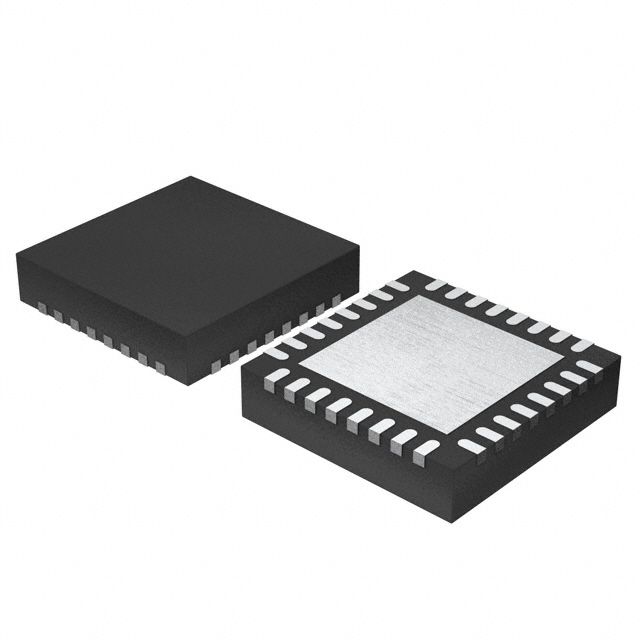
32-VFQFN package and supports industrial temperature range.
VCCX
XTAL_IN
XTAL_OUT
CLK0
nCLK0
VCC
CLK1
nCLK1
Pin Assignment
32
31
30
29
28
27
26
25
Two LVPECL output pairs
Each output supports independent frequency selection at 25MHz,
125MHz, 156.25MHz and 312.5MHz
Power supply noise rejection (PSNR): -85dB (typical)
FemtoClock NG VCXO frequency: 2500MHz
RMS phase jitter @ 156.25MHz, using a 27MHz crystal
(12kHz – 20MHz): 0.6ps (typical)
-40°C to 85°C ambient operating temperature
Available in lead-free (RoHS 6) package
LF1
1
24
VEE
LF0
2
23
nQB
ISET
3
22
QB
VEE
4
21
VCCO
CLK_SEL
5
20
nQA
VCC
6
19
QA
RESERVED
7
18
VEE
VEE
8
17
ODASEL_0
9
10
11
12
13
14
15
16
PDSEL_2
PDSEL_1
PDSEL_0
VCC
VCCA
ODBSEL_1
ODBSEL_0
ODASEL_1
813N252DI-02
32-pin, 5mm x 5mm VFQFN Package
REVISION 1 08/14/15
1
©2015 INTEGRATED DEVICE TECHNOLOGY, INC.
�813N252DI-02 DATA SHEET
Block Diagram
27MHz
Pulldown
DIGITAL
VCXO
Xtal
Osc.
2
ODASEL_[1:0]
QA
÷NA
nQA
PDSEL_[2:0]
CLK_SEL
Pullup
3
PD
+
LF
Pulldown
FemtoClock NG
VCO
QB
÷NB
CLK0
Pulldown
nCLK0
Pullup /
Pulldown
0
÷P
CLK1
nCLK1
Pulldown
Pullup /
Pulldown
1
nQB
Fractional
Feedback
Divider
Pulldown
Phase
Detector
+
Charge
Pump
2
ODBSEL_[1:0]
A / D Control
Block
REVISION 1 08/14/15
LF1
LF0
ISET
÷M
*** Dashed lines indicates external components
2
JITTER ATTENUATOR & FEMTOCLOCK NG® MULTIPLIER
�813N252DI-02 DATA SHEET
Pin Description and Pin Characteristic Tables
Table 1. Pin Descriptions
Number
Name
Type
Description
1, 2
LF1, LF0
Analog
Input/Output
Loop filter connection node pins. LF0 is the output. LF1 is the input.
3
ISET
Analog
Input/Output
Charge pump current setting pin.
4, 8, 18, 24
VEE
Power
5
CLK_SEL
Input
6, 12, 27
VCC
Power
7
RESERVED
Reserve
9,
10,
11
PDSEL_2,
PDSEL_1,
PDSEL_0
Input
13
VCCA
Power
14,
15
ODBSEL_1,
ODBSEL_0
Input
Pulldown
Frequency select pins for Bank B output. See Table 3B.
LVCMOS/LVTTL interface levels.
16,
17
ODASEL_1,
ODASEL_0
Input
Pulldown
Frequency select pins for Bank A output. See Table 3B.
LVCMOS/LVTTL interface levels.
19, 20
QA, nQA
Output
Differential Bank A clock outputs. LVPECL interface levels.
21
VCCO
Power
Output supply pin.
22, 23
QB, nQB
Output
Negative supply pins.
Pulldown
Input clock select. When HIGH selects CLK1, nCLK1. When LOW, selects
CLK0, nCLK0. LVCMOS / LVTTL interface levels.
Core supply pins.
Reserved pin.
Pullup
Pre-divider select pins. LVCMOS/LVTTL interface levels.
See Table 3A.
Analog supply pin.
Differential Bank B clock outputs. LVPECL interface levels.
25
nCLK1
Input
Pullup/
Pulldown
26
CLK1
Input
Pulldown
Non-inverting differential clock input.
28
nCLK0
Input
Pullup/
Pulldown
Inverting differential clock input. VCC/2 bias voltage when left floating.
29
CLK0
Input
Pulldown
Non-inverting differential clock input.
30,
31
XTAL_OUT,
XTAL_IN
Input
Crystal oscillator interface. XTAL_IN is the input. XTAL_OUT is the output.
32
VCCX
Power
Power supply pin for the crystal oscillator.
Inverting differential clock input. VCC/2 bias voltage when left floating.
NOTE: Pullup and Pulldown refer to internal input resistors. See Table 2, Pin Characteristics, for typical values.
Table 2. Pin Characteristics
Symbol
Parameter
CIN
Input Capacitance
2
pF
RPULLUP
Input Pullup Resistor
51
k
RPULLDOWN
Input Pulldown Resistor
51
k
JITTER ATTENUATOR & FEMTOCLOCK NG® MULTIPLIER
Test Conditions
3
Minimum
Typical
Maximum
Units
REVISION 1 08/14/15
�813N252DI-02 DATA SHEET
Function Tables
Table 3A. Pre-Divider Selection Function Table
Inputs
PDSEL_2
PDSEL_1
PDSEL_0
÷P Value
0
0
0
1
0
0
1
193
0
1
0
256
0
1
1
1944
1
0
0
2500
1
0
1
7776
1
1
0
12500
1
1
1
15552 (default)
Table 3B. Output Divider Function Table
Inputs
ODxSEL_1
ODxSEL_0
÷Nx Value
0
0
100 (default)
0
1
20
1
0
16
1
1
8
NOTE: x denotes A or B.
REVISION 1 08/14/15
4
JITTER ATTENUATOR & FEMTOCLOCK NG® MULTIPLIER
�813N252DI-02 DATA SHEET
Table 3C. Frequency Function Table
Input Frequency (MHz)
÷P Value
FemtoClock NG VCXO Center
Frequency (MHz)
÷Nx Value
Output Frequency (MHz)
0.008
1
2500
100
25
0.008
1
2500
20
125
0.008
1
2500
16
156.25
0.008
1
2500
8
312.5
1.544
193
2500
100
25
1.544
193
2500
20
125
1.544
193
2500
16
156.25
1.544
193
2500
8
312.5
2.048
256
2500
100
25
2.048
256
2500
20
125
2.048
256
2500
16
156.25
2.048
256
2500
8
312.5
19.44
1944
2500
100
25
19.44
1944
2500
20
125
19.44
1944
2500
16
156.25
19.44
1944
2500
8
312.5
25
2500
2500
100
25
25
2500
2500
20
125
25
2500
2500
16
156.25
25
2500
2500
8
312.5
77.76
7776
2500
100
25
77.76
7776
2500
20
125
77.76
7776
2500
16
156.25
77.76
7776
2500
8
312.5
125
12500
2500
100
25
125
12500
2500
20
125
125
12500
2500
16
156.25
125
12500
2500
8
312.5
155.52
15552
2500
100
25
155.52
15552
2500
20
125
155.52
15552
2500
16
156.25
155.52
15552
2500
8
312.5
NOTE: x denotes A or B.
JITTER ATTENUATOR & FEMTOCLOCK NG® MULTIPLIER
5
REVISION 1 08/14/15
�813N252DI-02 DATA SHEET
Absolute Maximum Ratings
NOTE: Stresses beyond those listed under Absolute Maximum Ratings may cause permanent damage to the device.
These ratings are stress specifications only. Functional operation of product at these conditions or any conditions beyond
those listed in the DC Characteristics or AC Characteristics is not implied. Exposure to absolute maximum rating conditions for
extended periods may affect product reliability.
Item
Rating
Supply Voltage, VCC
3.63V
Inputs, VI
XTAL_IN
Other Inputs
0V to 2V
-0.5V to VCC+ 0.5V
Outputs, IO
Continuous Current
Surge Current
50mA
100mA
Package Thermal Impedance, JA
33.1C/W (0 mps)
Storage Temperature, TSTG
-65C to 150C
DC Electrical Characteristics
Table 4A. LVPECL Power Supply DC Characteristics, VCC = VCCO = VCCX = 3.3V ± 5%, VEE = 0V, TA = -40°C to 85°C
Symbol
Parameter
Test Conditions
Minimum
Typical
Maximum
Units
VCC
Core Supply Voltage
3.135
3.3
3.465
V
VCCA
Analog Supply Voltage
VCC – 0.30
3.3
VCC
V
VCCO
Output Supply Voltage
3.135
3.3
3.465
V
VCCX
Crystal Supply Voltage
3.135
3.3
3.465
V
IEE
Power Supply Current
253
321
mA
ICCA
Analog Supply Current
30
mA
Maximum
Units
Table 4B. LVCMOS/LVTTL DC Characteristics, VCC = VCCO = VCCX = 3.3V ± 5%, TA = -40°C to 85°C
Symbol
Parameter
VIH
Input High Voltage
2
VCC + 0.3
V
VIL
Input Low Voltage
-0.3
0.8
V
IIH
IIL
Input
High Current
Input
Low Current
REVISION 1 08/14/15
Test Conditions
Minimum
Typical
CLK_SEL,
ODASEL_[1:0],
ODBSEL_[1:0]
VCC = VIN = 3.465V
150
µA
PDSEL_[2:0]
VCC = VIN = 3.465V
10
µA
CLK_SEL,
ODASEL_[1:0],
ODBSEL_[1:0]
VCC = 3.465V, VIN = 0V
-10
µA
PDSEL_[2:0]
VCC = 3.465, VIN = 0V
-150
µA
6
JITTER ATTENUATOR & FEMTOCLOCK NG® MULTIPLIER
�813N252DI-02 DATA SHEET
Table 4C. Differential DC Characteristics, VCC = VCCO = VCCX = 3.3V ± 5%, TA = -40°C to 85°C
Symbol
Parameter
Test Conditions
IIH
Input High Current
IIL
Input Low Current
VPP
Peak-to-Peak Input Voltage; NOTE 1
0.15
1.3
V
VCMR
Common Mode Input Voltage; NOTE 1, 2
VEE
VCC – 0.85
V
CLK0, nCLK0,
CLK1, nCLK1
Minimum
Typical
VCC = VIN = 3.465V
Maximum
Units
150
µA
CLK0, CLK1
VCC = 3.465V, VIN = 0V
-10
µA
nCLK0, nCLK1
VCC = 3.465V, VIN = 0V
-150
µA
NOTE 1: VIL should not be less than -0.3V.
NOTE 2. Common mode voltage is defined at the crosspoint.
Table 4D. LVPECL DC Characteristics, VCC = VCCO = VCCX = 3.3V ± 5%, VEE = 0V, TA = -40°C to 85°C
Symbol
Parameter
VOH
Output High Voltage; NOTE 1
VOL
Output Low Voltage; NOTE 1
VSWING
Peak-to-Peak Output Voltage Swing
Test Conditions
Minimum
Typical
Maximum
Units
VCCO – 1.10
VCCO – 0.75
V
VCCO – 2.0
VCCO – 1.6
V
0.6
1.0
V
NOTE 1: Outputs terminated with 50 to VCCO – 2V. See Parameter Measurement Information section, 3.3V Output Load Test Circuit.
JITTER ATTENUATOR & FEMTOCLOCK NG® MULTIPLIER
7
REVISION 1 08/14/15
�813N252DI-02 DATA SHEET
AC Electrical Characteristics
Table 5. AC Characteristics, VCC = VCCO = VCCX = 3.3V ± 5%, TA = -40°C to 85°C
Symbol
Parameter
fIN
Input Frequency
fOUT
Output Frequency
tjit(Ø)
RMS Phase Jitter, (Random),
NOTE 1
PSNR
Power Supply Noise Rejection;
NOTE 2
tsk(o)
Output Skew; NOTE 3, 4
tR / tF
Output Rise/Fall Time
odc
Output Duty Cycle
tLOCK
Output-to-Input Phase
Lock Time; NOTE 5
Test Conditions
Minimum
Typical
Maximum
Units
0.008
155.52
MHz
25
312.5
MHz
125MHz fOUT, 27MHz crystal,
Integration Range: 12kHz – 20MHz
0.65
ps
156.25MHz fOUT, 27MHz crystal,
Integration Range: 12kHz – 20MHz
0.6
ps
VPP = 50mV Sine Wave,
Range: 10kHz – 10MHz
-85
dB
20% to 80%
Reference Clock Input is ±100ppm from
Nominal Frequency
80
ps
150
450
ps
48
52
%
4
s
NOTE: Electrical parameters are guaranteed over the specified ambient operating temperature range, which is established when the device is
mounted in a test socket with maintained transverse airflow greater than 500 lfpm. The device will meet specifications after thermal equilibrium
has been reached under these conditions.
NOTE: Characterized with outputs at the same frequency using the loop filter components for the 35Hz loop bandwidth.
Refer to Jitter Attenuator Loop Bandwidth Selection Table.
NOTE 1: Refer to the Phase Noise Plot.
NOTE 2: PSNR results achieved by injecting noise on VCCA supply pin with no external filter network.
NOTE 3: This parameter is defined in accordance with JEDEC Standard 65.
NOTE 4: Defined as skew between outputs at the same supply voltage and with equal load conditions. Measured at the output differential
cross points.
NOTE 5: Lock Time measured from power-up to stable output frequency.
REVISION 1 08/14/15
8
JITTER ATTENUATOR & FEMTOCLOCK NG® MULTIPLIER
�813N252DI-02 DATA SHEET
Noise Power
dBc
Hz
Typical Phase Noise at 125MHz
Offset Frequency (Hz)
JITTER ATTENUATOR & FEMTOCLOCK NG® MULTIPLIER
9
REVISION 1 08/14/15
�813N252DI-02 DATA SHEET
Parameter Measurement Information
2V
2V
VCC
VCC,
VCCO,
VCCX
nCLK[0:1]
VCCA
V
PP
Cross Points
CLK[0:1]
V
CMR
VEE
-1.3V ± 0.165V
3.3V LVPECL Output Load AC Test Circuit
Differential Input Level
VCC
Supply Voltage
60% of VCC
VEE
Output-to-Input
Phase Lock
Output
Lock Time
Not to Scale
Output-to-Input Phase Lock Time
RMS Phase Jitter
nQx
nQA, nQB
Qx
nQy
QA, QB
Qy
LVPECL Output Rise/Fall Time
Output Skew
nQA, nQB
QA, QB
Output Duty Cycle/Pulse Width/Period
REVISION 1 08/14/15
10
JITTER ATTENUATOR & FEMTOCLOCK NG® MULTIPLIER
�813N252DI-02 DATA SHEET
Applications Information
Wiring the Differential Input to Accept Single-Ended Levels
Figure 1 shows how a differential input can be wired to accept single
ended levels. The reference voltage V1= VCC/2 is generated by the
bias resistors R1 and R2. The bypass capacitor (C1) is used to help
filter noise on the DC bias. This bias circuit should be located as close
to the input pin as possible. The ratio of R1 and R2 might need to be
adjusted to position the V1in the center of the input voltage swing. For
example, if the input clock is driven from a single-ended 2.5V
LVCMOS driver and the DC offset (or swing center) of this signal is
1.25V, the R1 and R2 values should be adjusted to set the V1 at
1.25V. The values below are for when both the single ended swing
and VCC are at the same voltage. This configuration requires that the
sum of the output impedance of the driver (Ro) and the series
resistance (Rs) equals the transmission line impedance. In addition,
matched termination at the input will attenuate the signal in half. This
can be done in one of two ways. First, R3 and R4 in parallel should
equal the transmission line impedance. For most 50 applications,
R3 and R4 can be 100. The values of the resistors can be increased
to reduce the loading for slower and weaker LVCMOS driver. When
using single-ended signaling, the noise rejection benefits of
differential signaling are reduced. Even though the differential input
can handle full rail LVCMOS signaling, it is recommended that the
amplitude be reduced while maintaining an edge rate faster than
1V/ns. The datasheet specifies a lower differential amplitude,
however this only applies to differential signals. For single-ended
applications, the swing can be larger, however VIL cannot be less
than -0.3V and VIH cannot be more than VCC + 0.3V. Though some
of the recommended components might not be used, the pads
should be placed in the layout. They can be utilized for debugging
purposes. The datasheet specifications are characterized and
guaranteed by using a differential signal.
Figure 1. Recommended Schematic for Wiring a Differential Input to Accept Single-ended Levels
JITTER ATTENUATOR & FEMTOCLOCK NG® MULTIPLIER
11
REVISION 1 08/14/15
�813N252DI-02 DATA SHEET
3.3V Differential Clock Input Interface
with the vendor of the driver component to confirm the driver
termination requirements. For example, in Figure 2A, the input
termination applies for IDT open emitter LVHSTL drivers. If you are
using an LVHSTL driver from another vendor, use their termination
recommendation.
The CLK /nCLK accepts LVDS, LVPECL, LVHSTL, HCSL and other
differential signals. Both differential inputs must meet the VPP and
VCMR input requirements. Figures 2A to 2E show interface examples
for the CLK /nCLK input driven by the most common driver types. The
input interfaces suggested here are examples only. Please consult
3.3V
1.8V
Zo = 50Ω
CLK
Zo = 50Ω
nCLK
Differential
Input
LVHSTL
R1
50Ω
IDT
LVHSTL Driver
R2
50Ω
Figure 2A. CLK/nCLK Input Driven by an
IDT Open Emitter LVHSTL Driver
Figure 2B. CLK/nCLK Input Driven by a
3.3V LVPECL Driver
Figure 2C. CLK/nCLK Input Driven by a
3.3V LVPECL Driver
Figure 2D. CLK/nCLK Input Driven by a
3.3V LVDS Driver
3.3V
3.3V
*R3
33Ω
Zo = 50Ω
CLK
Zo = 50Ω
nCLK
HCSL
*R4
33Ω
R1
50Ω
R2
50Ω
Differential
Input
*Optional – R3 and R4 can be 0Ω
Figure 2E. CLK/nCLK Input Driven by an HCSL Driver
REVISION 1 08/14/15
12
JITTER ATTENUATOR & FEMTOCLOCK NG® MULTIPLIER
�813N252DI-02 DATA SHEET
Recommendations for Unused Input and Output Pins
Inputs:
Outputs:
CLK/nCLK Inputs
LVPECL Outputs
For applications requiring only one differential input, the unused
CLKx and nCLKx pins can be left floating. Though not required, but
for additional protection, a 1k resistor can be tied from the unused
CLK input to ground.
All unused LVPECL outputs can be left floating. We recommend that
there is no trace attached. Both sides of the differential output pair
should either be left floating or terminated.
LVCMOS Control Pins
All control pins have internal pullups or pulldowns; additional
resistance is not required but can be added for additional protection.
A 1k resistor can be used.
Termination for 3.3V LVPECL Outputs
The clock layout topology shown below is a typical termination for
LVPECL outputs. The two different layouts mentioned are
recommended only as guidelines.
transmission lines. Matched impedance techniques should be used
to maximize operating frequency and minimize signal distortion.
Figures 3A and 3B show two different layouts which are
recommended only as guidelines. Other suitable clock layouts may
exist and it would be recommended that the board designers
simulate to guarantee compatibility across all printed circuit and clock
component process variations.
The differential output is a low impedance follower output that
generate ECL/LVPECL compatible outputs. Therefore, terminating
resistors (DC current path to ground) or current sources must be
used for functionality. These outputs are designed to drive 50
R3
125
3.3V
R4
125
3.3V
3.3V
Zo = 50
+
_
Input
Zo = 50
R1
84
Figure 3A. 3.3V LVPECL Output Termination
JITTER ATTENUATOR & FEMTOCLOCK NG® MULTIPLIER
R2
84
Figure 3B. 3.3V LVPECL Output Termination
13
REVISION 1 08/14/15
�813N252DI-02 DATA SHEET
Jitter Attenuator EXTERNAL COMPONENTS
Choosing the correct external components and having a proper
printed circuit board (PCB) layout is a key task for quality operation of
the Jitter Attenuator. In choosing a crystal, special precaution must
be taken with load capacitance (CL), frequency accuracy and
temperature range.
specification in the Crystal Characteristics Table are used to
calculate the APR (Absolute Pull Range). It is recommended that the
crystal CL not to exceed the value stated in the Crystal Parameter
Table because it can lead to a reduced APR
.
The crystal’s CL characteristic determines its resonating frequency
and is closely related to the center tuning of the crystal. The total
external capacitance (CEXTERNAL) seen by the crystal when installed
on a PCB is the sum of the stray board capacitance, IC package lead
capacitance, internal device capacitance and any installed tuning
capacitors (CTUNE). The recommended CLin the Crystal Parameter
Table balances the tuning range by centering the tuning curve for a
typical PCB. If the crystal CL is greater than the total external
capacitance (CL > CEXTERNAL), the crystal will oscillate at a higher
frequency than the specification. If the crystal CL is lower than the
total external capacitance (CL < CEXTERNAL), the crystal will oscillate
at a lower frequency than the specification. Mismatches between CL
and CEXTERNAL require adjustments in CTUNE in order to center the
tuning curve. For example, given a board with 5pF of stray
capacitance, CTUNE would be 0. In addition, the frequency accuracy
LF0
LF1
ISET
RS
CP
RSET
CS
XTAL_IN
CTUNE
27MHz
XTAL_OUT
CTUNE
Crystal Characteristics
Symbol
Parameter
Test Conditions
Minimum
fN
Frequency
fT
Frequency Tolerance
±20
ppm
fS
Frequency Stability
±20
ppm
+85
0C
Mode of Oscillation
Typical
Maximum
Units
Fundamental
27
Operating Temperature Range
MHz
-40
CL
Load Capacitance
10
pF
CO
Shunt Capacitance
4
pF
ESR
Equivalent Series Resistance
Drive Level
Aging @ 25
100
0C
First Year
40
1
µW
±3
ppm
Jitter Attenuator Characteristics Table
The VCXO-PLL Loop Bandwidth Selection Table shows RS, CS,CP
and RSET values for recommended high, mid and low loop bandwidth
configurations. The device has been characterized using these
parameters. In addition, the digital VCXO gain (kVCXO) has been
provided for additional loop filter requirements.
Symbol
Parameter
Typical
Units
kVCXO
VCXO Gain
2.6
kHz/V
Jitter Attenuator Loop Bandwidth Selection Table
Bandwidth
Crystal Frequency
RS (k)
CS (µF)
CP (µF)
RSET (k)
7Hz (Low)
27MHz
110
10
0.01
2.21
35Hz (Mid)
27MHz
365
1
0.002
1.5
45Hz (High)
27MHz
470
1
0.0005
1.5
The crystal and external loop filter components should be kept as
close as possible to the device. Loop filter and crystal traces should
be kept short and separated from each other. Other signal traces
REVISION 1 08/14/15
should be kept separate and not run underneath the device, loop filter
or crystal components.
14
JITTER ATTENUATOR & FEMTOCLOCK NG® MULTIPLIER
�813N252DI-02 DATA SHEET
VFQFN EPAD Thermal Release Path
In order to maximize both the removal of heat from the package and
the electrical performance, a land pattern must be incorporated on
the Printed Circuit Board (PCB) within the footprint of the package
corresponding to the exposed metal pad or exposed heat slug on the
package, as shown in Figure 4. The solderable area on the PCB, as
defined by the solder mask, should be at least the same size/shape
as the exposed pad/slug area on the package to maximize the
thermal/electrical performance. Sufficient clearance should be
designed on the PCB between the outer edges of the land pattern
and the inner edges of pad pattern for the leads to avoid any shorts.
and dependent upon the package power dissipation as well as
electrical conductivity requirements. Thus, thermal and electrical
analysis and/or testing are recommended to determine the minimum
number needed. Maximum thermal and electrical performance is
achieved when an array of vias is incorporated in the land pattern. It
is recommended to use as many vias connected to ground as
possible. It is also recommended that the via diameter should be 12
to 13mils (0.30 to 0.33mm) with 1oz copper via barrel plating. This is
desirable to avoid any solder wicking inside the via during the
soldering process which may result in voids in solder between the
exposed pad/slug and the thermal land. Precautions should be taken
to eliminate any solder voids between the exposed heat slug and the
land pattern. Note: These recommendations are to be used as a
guideline only. For further information, please refer to the Application
Note on the Surface Mount Assembly of Amkor’s
Thermally/Electrically Enhance Leadframe Base Package, Amkor
Technology.
While the land pattern on the PCB provides a means of heat transfer
and electrical grounding from the package to the board through a
solder joint, thermal vias are necessary to effectively conduct from
the surface of the PCB to the ground plane(s). The land pattern must
be connected to ground through these vias. The vias act as “heat
pipes”. The number of vias (i.e. “heat pipes”) are application specific
PIN
PIN PAD
SOLDER
EXPOSED HEAT SLUG
GROUND PLANE
THERMAL VIA
SOLDER
LAND PATTERN
(GROUND PAD)
PIN
PIN PAD
Figure 4. P.C. Assembly for Exposed Pad Thermal Release Path – Side View (drawing not to scale)
JITTER ATTENUATOR & FEMTOCLOCK NG® MULTIPLIER
15
REVISION 1 08/14/15
�813N252DI-02 DATA SHEET
Schematic Example
Figure 5 (on next page) shows an example of 813N252DI-02
application schematic. In this example, the device is operated at VCC
= VCCX = VCCO = 3.3V. A 10pF parallel resonant 27MHz crystal is
used. Spare placement pads for the load capacitance C1 and C2 are
recommended for frequency accuracy. Depending on the parasitics
of the printed circuit board layout, these values might require a slight
adjustment to optimize the frequency accuracy. Crystals with other
load capacitance specifications can be used. This will required
adjusting C1 and C2.
In order to achieve the best possible filtering, it is recommended that
the placement of the filter components be on the device side of the
PCB as close to the power pins as possible. If space is limited, the
0.1µF capacitor in each power pin filter should be placed on the
device side of the PCB and the other components can be placed on
the opposite side.
Power supply filter recommendations are a general guideline to be
used for reducing external noise from coupling into the devices. The
filter performance is designed for wide range of noise frequencies.
This low-pass filter starts to attenuate noise at approximately 10kHz.
If a specific frequency noise component is known, such as switching
power supply frequencies, it is recommended that component values
be adjusted and if required, additional filtering be added. Additionally,
good general design practices for power plane voltage stability
suggests adding bulk capacitances in the local area of all devices.
An Optional 3-pole filter can also be used for additional spur
reduction. It is recommended that the loop filter components be laid
out for the 3-pole option. This will allow the flexibility for the 2-pole
filter to be used.
As with any high speed analog circuitry, the power supply pins are
vulnerable to noise. To achieve optimum jitter performance, power
supply isolation is required. The 813N252DI-02 provides separate
power supplies to isolate from coupling into the internal PLL.
REVISION 1 08/14/15
The schematic example focuses on functional connections and is not
configuration specific. Refer to the pin description and functional
tables in the datasheet to ensure the logic control inputs are properly
set.
16
JITTER ATTENUATOR & FEMTOCLOCK NG® MULTIPLIER
�813N252DI-02 DATA SHEET
VCC
R1
125
VCC
Logic Control Input Examples
R2
125
Zo = 50
Set Logic
Input to
'1'
VCC
CLK1
R5
125
R6
125
nCLK1
Zo = 50
LVPECL Driv er
R20
84
nCLK0
RU1
1K
RU2
Not Install
To Logic
Input
pins
CLK0
Zo = 50
R4
84
To Logic
Input
pins
RD1
Not Install
Zo = 50
R7
84
LVPECL Driv er
Set Logic
Input to
'0'
VCC
RD2
1K
R8
85
3-pole loop filter example - (optional)
R3
LF
LF
3.3V
XTAL_OUT
Rs
365k
3.3V
820k
C1
TUNE
C3
220pF
F
p
0
1
Cp
0.002uF
Cs
1uF
1
27MHz
X1
BLM18BB221SN1
2
Ferrite Bead C6
C5
0.1uF
R9
133
R10
133
Zo = 50 Ohm
10uF
XTAL_IN
+
C LK1
nC LK1
C2
TUNE
VCC
C LK0
nC LK0
Zo = 50 Ohm
R11
10
VCC
VCCX
R12
82.5
U1
2-pole loop filter for Mid Bandwidth setting
LF
1
2
3
4
5
6
7
8
Rs
365k
VCC
3.3V
R14
1.5K
BLM18BB221SN1
1
VEE
nQB
QB
VCCO
nQA
QA
VEE
ODASEL_0
nQB
QB
nQA
QA
VCC
2
10uF
+
R15
50
LVPECL
Optional
Y-Termination
VCCA
C6
Zo = 50 Ohm
ODASEL_0
Zo = 50 Ohm
Ferrite Bead
C5
0.1uF
24
23
22
21
20
19
18
17
9
10
11
12
13
OD BSEL_1 14
OD BSEL_0 15
OD ASEL_1 16
C7
0.1u
LVPECL
Termination
PD SEL2
PD SEL_1
PD SEL_0
VC C
VC C A
OD BSEL_1
OD BSEL_0
OD ASEL_1
CLK_SEL
Cp
0.002uF
C6
PD SEL_2
PD SEL_1
PD SEL_0
Cs
1uF
LF1
LF0
ISET
VEE
CLK_SEL
VCC
RESERVED
VEE
R13
82.5
VCCO
0.1u
32
31
30
29
28
27
26
25
C5
10u
VC C X
XT AL_IN
XT AL_OU T
C LK0
nC LK0
VC C
C LK1
nC LK1
C4
0.1u
LF
-
C11
0.1u
R19
10
R16
50
R18
50
VCC
C8
0.1u
C9
0.1u
C10
10u
Figure 5. 813N252DI-02 Schematic Example
JITTER ATTENUATOR & FEMTOCLOCK NG® MULTIPLIER
17
REVISION 1 08/14/15
�813N252DI-02 DATA SHEET
Power Considerations
This section provides information on power dissipation and junction temperature for the 813N252DI-02.
Equations and example calculations are also provided.
1.
Power Dissipation.
The total power dissipation for the 813N252DI-02 is the sum of the core power plus the power dissipated in the load(s).
The following is the power dissipation for VCCO = 3.3V + 5% = 3.465V, which gives worst case results.
NOTE: Please refer to Section 3 for details on calculating power dissipated in the load.
•
Power (core)MAX = VCCO_MAX * IEE_MAX = 3.465V * 321mA = 1112.3mW
•
Power (outputs)MAX = 31.55mW/Loaded Output pair
If all outputs are loaded, the total power is 2 * 31.55mW = 63.1mW
Total Power_MAX (3.465V, with all outputs switching) = 1112.3mW + 63.1mW = 1175.4mW
2. Junction Temperature.
Junction temperature, Tj, is the temperature at the junction of the bond wire and bond pad directly affects the reliability of the device. The
maximum recommended junction temperature is 125°C. Limiting the internal transistor junction temperature, Tj, to 125°C ensures that the bond
wire and bond pad temperature remains below 125°C.
The equation for Tj is as follows: Tj = JA * Pd_total + TA
Tj = Junction Temperature
JA = Junction-to-Ambient Thermal Resistance
Pd_total = Total Device Power Dissipation (example calculation is in section 1 above)
TA = Ambient Temperature
In order to calculate junction temperature, the appropriate junction-to-ambient thermal resistance JA must be used. Assuming no air flow and
a multi-layer board, the appropriate value is 33.1°C/W per Table 6 below.
Therefore, Tj for an ambient temperature of 85°C with all outputs switching is:
85°C +1.175W * 33.1°C/W = 123.9°C. This is below the limit of 125°C.
This calculation is only an example. Tj will obviously vary depending on the number of loaded outputs, supply voltage, air flow and the type of
board (multi-layer).
Table 6. Thermal Resistance JA for 32 Lead VFQFN, Forced Convection
JA by Velocity
Meters per Second
Multi-Layer PCB, JEDEC Standard Test Boards
REVISION 1 08/14/15
0
1
3
33.1°C/W
28.1°C/W
25.4°C/W
18
JITTER ATTENUATOR & FEMTOCLOCK NG® MULTIPLIER
�813N252DI-02 DATA SHEET
3. Calculations and Equations.
The purpose of this section is to calculate the power dissipation for the LVPECL output pair.
LVPECL output driver circuit and termination are shown in Figure 6.
VCCO
Q1
VOUT
RL
50Ω
VCCO - 2V
Figure 6. LVPECL Driver Circuit and Termination
o calculate worst case power dissipation into the load, use the following equations which assume a 50 load, and a termination voltage of
VCCO – 2V.
•
For logic high, VOUT = VOH_MAX = VCCO_MAX – 0.75V
(VCC_MAX – VOH_MAX) = 0.75V
•
For logic low, VOUT = VOL_MAX = VCCO_MAX – 1.6V
(VCC_MAX – VOL_MAX) = 1.6V
Pd_H is power dissipation when the output drives high.
Pd_L is the power dissipation when the output drives low.
Pd_H = [(VOH_MAX – (VCCO_MAX – 2V))/RL] * (VCCO_MAX – VOH_MAX) = [(2V– (VCCO_MAX – VOH_MAX))/RL] * (VCCO_MAX – VOH_MAX) =
[(2V– 0.75V)/50] * 0.75V = 18.75mW
Pd_L = [(VOL_MAX – (VCCO_MAX – 2V))/RL] * (VCCO_MAX – VOL_MAX) = [(2V – (VCCO_MAX – VOL_MAX))/RL] * (VCCO_MAX – VOL_MAX) =
[(2V – 1.6V)/50] * 1.6V = 12.80mW
Total Power Dissipation per output pair = Pd_H + Pd_L = 31.55mW
JITTER ATTENUATOR & FEMTOCLOCK NG® MULTIPLIER
19
REVISION 1 08/14/15
�813N252DI-02 DATA SHEET
Reliability Information
Table 7. JA vs. Air Flow Table for a 32 Lead VFQFN
JA vs. Air Flow
Meters per Second
Multi-Layer PCB, JEDEC Standard Test Boards
0
1
3
33.1°C/W
28.1°C/W
25.4°C/W
Transistor Count
The transistor count for 813N252DI-02 is: 45,491
REVISION 1 08/14/15
20
JITTER ATTENUATOR & FEMTOCLOCK NG® MULTIPLIER
�813N252DI-02 DATA SHEET
Package Outline and Package Dimensions
Package Outline - K Suffix for 32 Lead VFQFN
(Ref.)
S eating Plan e
N &N
Even
(N -1)x e
(R ef.)
A1
Ind ex Area
L
A3
N
N
Anvil
Anvil
Singulation
Singula tion
e (Ty p.)
2 If N & N
1
are Even
2
OR
E2
(N -1)x e
(Re f.)
E2
2
To p View
b
A
(Ref.)
D
Chamfer 4x
0.6 x 0.6 max
OPTIONAL
e
N &N
Odd
0. 08
C
Bottom View w/Type A ID
4
Th er mal
Ba se
D2
C
Bottom View w/Type C ID
2
1
2
1
CHAMFER
D2
2
N N-1
RADIUS
4
N N-1
There are 2 methods of indicating pin 1 corner at the back of the VFQFN package:
1. Type A: Chamfer on the paddle (near pin 1)
2. Type C: Mouse bite on the paddle (near pin 1)
Table 8. Package Dimensions
NOTE: The following package mechanical drawing is a generic
drawing that applies to any pin count VFQFN package. This drawing
is not intended to convey the actual pin count or pin layout of this
device. The pin count and pin-out are shown on the front page. The
package dimensions are in Table 8.
JEDEC Variation: VHHD-2/-4
All Dimensions in Millimeters
Symbol
Minimum
Nominal
Maximum
N
32
A
0.80
1.00
A1
0
0.05
A3
0.25 Ref.
b
0.18
0.25
0.30
8
ND & NE
D&E
5.00 Basic
D2 & E2
3.0
3.3
e
0.50 Basic
L
0.30
0.40
0.50
Reference Document: JEDEC Publication 95, MO-220
JITTER ATTENUATOR & FEMTOCLOCK NG® MULTIPLIER
21
REVISION 1 08/14/15
�813N252DI-02 DATA SHEET
Ordering Information
Table 9. Ordering Information
Part/Order Number
Marking
Package
Shipping Packaging
Temperature
813N252DKI-02LF
ICSN52DI02L
32 Lead VFQFN, Lead-Free
Tray
-40°C to 85°C
813N252DKI-02LFT
ICSN52DI02L
32 Lead VFQFN, Lead-Free
Tape & Reel
-40°C to 85°C
REVISION 1 08/14/15
22
JITTER ATTENUATOR & FEMTOCLOCK NG® MULTIPLIER
�Corporate Headquarters
Sales
Tech Support
6024 Silver Creek Valley Road
San Jose, CA 95138 USA
1-800-345-7015 or 408-284-8200
Fax: 408-284-2775
www.IDT.com
email: clocks@idt.com
DISCLAIMER Integrated Device Technology, Inc. (IDT) and its subsidiaries reserve the right to modify the products and/or specifications described herein at any time and at IDT’s sole discretion. All information in
this document, including descriptions of product features and performance, is subject to change without notice. Performance specifications and the operating parameters of the described products are determined
in the independent state and are not guaranteed to perform the same way when installed in customer products. The information contained herein is provided without representation or warranty of any kind, whether
express or implied, including, but not limited to, the suitability of IDT’s products for any particular purpose, an implied warranty of merchantability, or non-infringement of the intellectual property rights of others. This
document is presented only as a guide and does not convey any license under intellectual property rights of IDT or any third parties.
IDT’s products are not intended for use in applications involving extreme environmental conditions or in life support systems or similar devices where the failure or malfunction of an IDT product can be reasonably
expected to significantly affect the health or safety of users. Anyone using an IDT product in such a manner does so at their own risk, absent an express, written agreement by IDT.
Integrated Device Technology, IDT and the IDT logo are registered trademarks of IDT. Product specification subject to change without notice. Other trademarks and service marks used herein, including protected
names, logos and designs, are the property of IDT or their respective third party owners.
Copyright ©2015 Integrated Device Technology, Inc. All rights reserved.
�IMPORTANT NOTICE AND DISCLAIMER
RENESAS ELECTRONICS CORPORATION AND ITS SUBSIDIARIES (“RENESAS”) PROVIDES TECHNICAL
SPECIFICATIONS AND RELIABILITY DATA (INCLUDING DATASHEETS), DESIGN RESOURCES (INCLUDING
REFERENCE DESIGNS), APPLICATION OR OTHER DESIGN ADVICE, WEB TOOLS, SAFETY INFORMATION, AND
OTHER RESOURCES “AS IS” AND WITH ALL FAULTS, AND DISCLAIMS ALL WARRANTIES, EXPRESS OR IMPLIED,
INCLUDING, WITHOUT LIMITATION, ANY IMPLIED WARRANTIES OF MERCHANTABILITY, FITNESS FOR A
PARTICULAR PURPOSE, OR NON-INFRINGEMENT OF THIRD PARTY INTELLECTUAL PROPERTY RIGHTS.
These resources are intended for developers skilled in the art designing with Renesas products. You are solely responsible
for (1) selecting the appropriate products for your application, (2) designing, validating, and testing your application, and (3)
ensuring your application meets applicable standards, and any other safety, security, or other requirements. These
resources are subject to change without notice. Renesas grants you permission to use these resources only for
development of an application that uses Renesas products. Other reproduction or use of these resources is strictly
prohibited. No license is granted to any other Renesas intellectual property or to any third party intellectual property.
Renesas disclaims responsibility for, and you will fully indemnify Renesas and its representatives against, any claims,
damages, costs, losses, or liabilities arising out of your use of these resources. Renesas' products are provided only subject
to Renesas' Terms and Conditions of Sale or other applicable terms agreed to in writing. No use of any Renesas resources
expands or otherwise alters any applicable warranties or warranty disclaimers for these products.
(Rev.1.0 Mar 2020)
Corporate Headquarters
Contact Information
TOYOSU FORESIA, 3-2-24 Toyosu,
Koto-ku, Tokyo 135-0061, Japan
www.renesas.com
For further information on a product, technology, the most
up-to-date version of a document, or your nearest sales
office, please visit:
www.renesas.com/contact/
Trademarks
Renesas and the Renesas logo are trademarks of Renesas
Electronics Corporation. All trademarks and registered
trademarks are the property of their respective owners.
© 2020 Renesas Electronics Corporation. All rights reserved.
�


 工商网监
湘ICP备2023018690号
工商网监
湘ICP备2023018690号
