SINGLE CHANNEL T1/E1/J1
SHORT HAUL LINE INTERFACE UNIT
IDT82V2041E
FEATURES
•
•
•
•
•
•
Single channel T1/E1/J1 short haul line interfaces
Supports HPS (Hitless Protection Switching) for 1+1 protection
without external relays
Programmable T1/E1/J1 switchability allowing one bill of material for any line condition
Single 3.3 V power supply with 5 V tolerance on digital interfaces
Meets or exceeds specifications in
- ANSI T1.102, T1.403 and T1.408
- ITU I.431, G.703, G.736, G.775 and G.823
- ETSI 300-166, 300-233 and TBR12/13
- AT&T Pub 62411
Software programmable or hardware selectable on:
- Wave-shaping templates
- Line terminating impedance (T1:100 Ω, J1:110 Ω, E1:75 Ω/120 Ω)
- Adjustment of arbitrary pulse shape
- JA (Jitter Attenuator) position (receive path or transmit path)
- Single rail/dual rail system interfaces
- B8ZS/HDB3/AMI line encoding/decoding
- Active edge of transmit clock (TCLK) and receive clock (RCLK)
- Active level of transmit data (TDATA) and receive data (RDATA)
- Receiver or transmitter power down
- High impedance setting for line drivers
•
•
•
•
•
•
•
- PRBS (Pseudo Random Bit Sequence) generation and detection
with 215-1 PRBS polynomials for E1
- QRSS (Quasi Random Sequence Signals) generation and detection
with 220-1 QRSS polynomials for T1/J1
- 16-bit BPV (Bipolar Pulse Violation) /Excess Zero/PRBS or QRSS
error counter
- Analog loopback, Digital loopback, Remote loopback and Inband
loopback
Adaptive receive sensitivity up to -20 dB (Host Mode only)
Short circuit protection and internal protection diode for line
drivers
LOS (Loss Of Signal) detection with programmable LOS levels
(Host Mode only)
AIS (Alarm Indication Signal) detection
Supports serial control interface, Motorola and Intel Multiplexed
interfaces and hardware control mode
Pin compatibe to 82V2081 T1/E1/J1 Long Haul/Short Haul LIU
and 82V2051E E1 Short Haul LIU
Package:
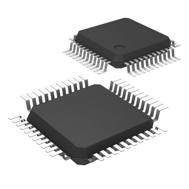
Available in 44-pin TQFP packages
Green package options available
DESCRIPTION
The IDT82V2041E can be configured as a single channel T1, E1 or J1
Line Interface Unit. The IDT82V2041E performs clock/data recovery, AMI/
B8ZS/HDB3 line decoding and detects and reports the LOS conditions. An
integrated Adaptive Equalizer is available to increase the receive sensitivity
and enable programming of LOS levels. In transmit path, there is an AMI/
B8ZS/HDB3 encoder and Waveform Shaper. There is one Jitter Attenuator, which can be placed in either the receive path or the transmit path. The
Jitter Attenuator can also be disabled. The IDT82V2041E supports both
Single Rail and Dual Rail system interfaces. To facilitate the network maintenance, a PRBS/QRSS generation/detection circuit is integrated in the
chip, and different types of loopbacks can be set according to the applications. Four different kinds of line terminating impedance, 75 Ω, 100 Ω, 110
Ω and 120 Ω are selectable. The chip also provides driver short-circuit protection and internal protection diode. The chip can be controlled by either
software or hardware.
The IDT82V2041E can be used in LAN, WAN, Routers, Wireless Base
Stations, IADs, IMAs, IMAPs, Gateways, Frame Relay Access Devices,
CSU/DSU equipment, etc.
1
December 9, 2005
DSC-6775/1
�IDT82V2041E
SINGLE CHANNEL T1/E1/J1 SHORT HAUL LINE INTERFACE UNIT
FUNCTIONAL BLOCK DIAGRAM
LOS/AIS
Detector
LOS
RCLK
RD/RDP
CV/RDN
B8ZS/
HDB3/AMI
Decoder
PRBS Detector
Remote
Loopback
IBLC Detector
TCLK
TD/TDP
TDN
Data and
Clock
Recovery
Jitter
Attenuator
B8ZS/
HDB3/AMI
Decoder
Adaptive
Equalizer
Data
Slicer
Receiver
Internal
Termination
RRING
Analog
Loopback
Digital
Loopback
Jitter
Attenuator
RTIP
TTIP
Transmitter
Internal
Termination
Line
Driver
Waveform
Shaper
TRING
PRBS Generator
IBLC Generator
TAOS
Register
Files
Pin Control
MODE[1:0]
TERM
RXTXM[1:0]
PULS[3:0]
PATT[1:0]
JA[1:0]
MONT
LP[1:0]
THZ
RCLKE
RPD
RST
AD[7:0]
SDI/ WR /R/W
RD / DS / SCLKE
SCLK/ALE/AS
SDO / ACK / RDY
CS
Software Control Interface
INT
MCLK
Clock
Generator
VDDIO
VDDD
VDDA
VDDT
Figure-1 Block Diagram
Functional Block Diagram
2
December 9, 2005
�Table of Contents
1
IDT82V2041E Pin Configurations ............................................................................................... 8
2
Pin Description ............................................................................................................................ 9
3
Functional Description .............................................................................................................. 15
3.1
Control Mode Selection .................................................................................................... 15
3.2
T1/E1/J1 Mode Selection .................................................................................................. 15
3.3
Transmit Path ................................................................................................................... 15
3.3.1 Transmit Path System Interface.............................................................................. 15
3.3.2 Encoder.................................................................................................................. 15
3.3.3 Pulse Shaper .......................................................................................................... 15
3.3.3.1 Preset Pulse Templates .......................................................................... 15
3.3.3.2 User-Programmable Arbitrary Waveform ................................................ 17
3.3.4 Transmit Path Line Interface................................................................................... 20
3.3.5 Transmit Path Power Down .................................................................................... 20
3.4
Receive Path .................................................................................................................... 21
3.4.1 Receive Internal Termination .................................................................................. 21
3.4.2 Line Monitor ............................................................................................................ 22
3.4.3 Adaptive Equalizer .................................................................................................. 23
3.4.4 Receive Sensitivity.................................................................................................. 23
3.4.5 Data Slicer .............................................................................................................. 23
3.4.6 CDR (Clock & Data Recovery)................................................................................ 23
3.4.7 Decoder .................................................................................................................. 23
3.4.8 Receive Path System Interface............................................................................... 24
3.4.9 Receive Path Power Down ..................................................................................... 24
3.5
Jitter Attenuator ................................................................................................................ 24
3.5.1 Jitter Attenuation Function Descripton .................................................................... 24
3.5.2 Jitter Attenuator Performance ................................................................................. 25
3.6
Los And AIS Detection ...................................................................................................... 25
3.6.1 LOS Detection......................................................................................................... 25
3.6.2 AIS Detection .......................................................................................................... 26
3.7
Transmit And Detect Internal Patterns .............................................................................. 28
3.7.1 Transmit All Ones ................................................................................................... 28
3.7.2 Transmit All Zeros................................................................................................... 28
3.7.3 PRBS/QRSS Generation And Detection................................................................. 28
3.8
Loopback .......................................................................................................................... 28
3.8.1 Analog Loopback .................................................................................................... 28
3.8.2 Digital Loopback ..................................................................................................... 28
3.8.3 Remote Loopback................................................................................................... 28
Table of Contents
3
December 9, 2005
�IDT82V2041E
3.9
3.10
3.11
3.12
3.13
3.14
3.15
3.16
SINGLE CHANNEL T1/E1/J1 SHORT HAUL LINE INTERFACE UNIT
3.8.4 Inband Loopback .................................................................................................... 30
3.8.4.1 Transmit Activate/Deactivate Loopback Code......................................... 30
3.8.4.2 Receive Activate/Deactivate Loopback Code.......................................... 30
3.8.4.3 Automatic Remote Loopback .................................................................. 31
Error Detection/Counting And Insertion ............................................................................ 32
3.9.1 Definition Of Line Coding Error ............................................................................... 32
3.9.2 Error Detection And Counting ................................................................................. 32
3.9.3 Bipolar Violation And PRBS Error Insertion ............................................................ 33
Line Driver Failure Monitoring ........................................................................................... 33
MCLK And TCLK .............................................................................................................. 34
3.11.1 Master Clock (MCLK).............................................................................................. 34
3.11.2 Transmit Clock (TCLK) ........................................................................................... 34
Microcontroller Interfaces ................................................................................................. 35
3.12.1 Parallel Microcontroller Interface ............................................................................ 35
3.12.2 Serial Microcontroller Interface ............................................................................... 35
Interrupt Handling ............................................................................................................. 35
5V Tolerant I/O Pins ......................................................................................................... 36
Reset Operation ................................................................................................................ 36
Power Supply .................................................................................................................... 36
4
Programming Information ........................................................................................................ 37
4.1
Register List And Map ...................................................................................................... 37
4.2
Reserved Registers .......................................................................................................... 37
4.3
Register Description ......................................................................................................... 38
4.3.1 Control Registers .................................................................................................... 38
4.3.2 Transmit Path Control Registers............................................................................. 40
4.3.3 Receive Path Control Registers.............................................................................. 42
4.3.4 Network Diagnostics Control Registers .................................................................. 44
4.3.5 Interrupt Control Registers...................................................................................... 47
4.3.6 Line Status Registers.............................................................................................. 50
4.3.7 Interrupt Status Registers ....................................................................................... 52
4.3.8 Counter Registers ................................................................................................... 54
5
Hardware Control Pin Summary .............................................................................................. 55
6
Test Specifications .................................................................................................................... 57
7
Microcontroller Interface Timing Characteristics ................................................................... 70
7.1
Serial Interface Timing ...................................................................................................... 70
7.2
Parallel Interface Timing ................................................................................................... 71
Table of Contents
4
December 9, 2005
�List of Tables
Table-1
Table-2
Table-3
Table-4
Table-5
Table-6
Table-7
Table-8
Table-9
Table-10
Table-11
Table-12
Table-13
Table-14
Table-15
Table-16
Table-17
Table-18
Table-19
Table-20
Table-21
Table-22
Table-23
Table-24
Table-25
Table-26
Table-27
Table-28
Table-29
Table-30
Table-31
Table-32
Table-33
Table-34
Table-35
Table-36
Table-37
Table-38
Table-39
Table-40
Table-41
List of Tables
Pin Description ................................................................................................................ 9
Transmit Waveform Value For E1 75 ohm.................................................................... 17
Transmit Waveform Value For E1 120 ohm.................................................................. 18
Transmit Waveform Value For T1 0~133 ft................................................................... 18
Transmit Waveform Value For T1 133~266 ft............................................................... 18
Transmit Waveform Value For T1 266~399 ft............................................................... 18
Transmit Waveform Value For T1 399~533 ft............................................................... 19
Transmit Waveform Value For T1 533~655 ft............................................................... 19
Transmit Waveform Value For J1 0~655 ft ................................................................... 19
Impedance Matching for Transmitter ............................................................................ 20
Impedance Matching for Receiver ................................................................................ 21
Criteria of Starting Speed Adjustment........................................................................... 25
LOS Declare and Clear ................................................................................................ 26
LOS Declare and Clear Criteria, Adaptive Equalizer Enabled ...................................... 26
AIS Condition ................................................................................................................ 27
Criteria for Setting/Clearing the PRBS_S Bit ................................................................ 28
EXZ Definition ............................................................................................................... 32
Interrupt Event............................................................................................................... 36
Register List and Map ................................................................................................... 37
ID: Device Revision Register ........................................................................................ 38
RST: Reset Register ..................................................................................................... 38
GCF: Global Configuration Register ............................................................................. 38
TERM: Transmit and Receive Termination Configuration Register .............................. 38
JACF: Jitter Attenuation Configuration Register ........................................................... 39
TCF0: Transmitter Configuration Register 0 ................................................................. 40
TCF1: Transmitter Configuration Register 1 ................................................................. 40
TCF2: Transmitter Configuration Register 2 ................................................................. 41
TCF3: Transmitter Configuration Register 3 ................................................................. 41
TCF4: Transmitter Configuration Register 4 ................................................................. 41
RCF0: Receiver Configuration Register 0..................................................................... 42
RCF1: Receiver Configuration Register 1..................................................................... 42
RCF2: Receiver Configuration Register 2..................................................................... 43
MAINT0: Maintenance Function Control Register 0...................................................... 44
MAINT1: Maintenance Function Control Register 1...................................................... 44
MAINT2: Maintenance Function Control Register 2...................................................... 45
MAINT3: Maintenance Function Control Register 3...................................................... 45
MAINT4: Maintenance Function Control Register 4...................................................... 45
MAINT5: Maintenance Function Control Register 5...................................................... 45
MAINT6: Maintenance Function Control Register 6...................................................... 46
INTM0: Interrupt Mask Register 0 ................................................................................. 47
INTM1: Interrupt Masked Register 1 ............................................................................. 48
5
December 9, 2005
�IDT82V2041E
Table-42
Table-43
Table-44
Table-45
Table-46
Table-47
Table-48
Table-49
Table-50
Table-51
Table-52
Table-53
Table-54
Table-55
Table-56
Table-57
Table-58
Table-59
Table-60
Table-61
Table-62
Table-63
Table-64
Table-65
List of Tables
SINGLE CHANNEL T1/E1/J1 SHORT HAUL LINE INTERFACE UNIT
INTES: Interrupt Trigger Edge Select Register .............................................................
STAT0: Line Status Register 0 (real time status monitor).............................................
STAT1: Line Status Register 1 (real time status monitor).............................................
INTS0: Interrupt Status Register 0 ................................................................................
INTS1: Interrupt Status Register 1 ................................................................................
CNT0: Error Counter L-byte Register 0.........................................................................
CNT1: Error Counter H-byte Register 1 ........................................................................
Hardware Control Pin Summary ...................................................................................
Absolute Maximum Rating ............................................................................................
Recommended Operation Conditions ...........................................................................
Power Consumption......................................................................................................
DC Characteristics ........................................................................................................
E1 Receiver Electrical Characteristics ..........................................................................
T1/J1 Receiver Electrical Characteristics......................................................................
E1 Transmitter Electrical Characteristics ......................................................................
T1/J1 Transmitter Electrical Characteristics..................................................................
Transmitter and Receiver Timing Characteristics .........................................................
Jitter Tolerance .............................................................................................................
Jitter Attenuator Characteristics ....................................................................................
Serial Interface Timing Characteristics .........................................................................
Multiplexed Motorola Read Timing Characteristics.......................................................
Multiplexed Motorola Write Timing Characteristics .......................................................
Multiplexed Intel Read Timing Characteristics ..............................................................
Multiplexed Intel Write Timing Characteristics ..............................................................
6
49
50
51
52
53
54
54
55
57
57
58
58
59
60
61
62
63
64
67
70
71
72
73
74
December 9, 2005
�List of Figures
Figure-1
Figure-2
Figure-3
Figure-4
Figure-5
Figure-6
Figure-7
Figure-8
Figure-9
Figure-10
Figure-11
Figure-12
Figure-13
Figure-14
Figure-15
Figure-16
Figure-17
Figure-18
Figure-19
Figure-20
Figure-21
Figure-22
Figure-23
Figure-24
Figure-25
Figure-26
Figure-27
Figure-28
Figure-29
Figure-30
Figure-31
Figure-32
List of Figures
Block Diagram ................................................................................................................. 2
IDT82V2041E TQFP44 Package Pin Assignment .......................................................... 8
E1 Waveform Template Diagram .................................................................................. 16
E1 Pulse Template Test Circuit ..................................................................................... 16
DSX-1 Waveform Template .......................................................................................... 16
T1 Pulse Template Test Circuit ..................................................................................... 16
Receive Monitor Gain Adaptive Equalizer ..................................................................... 21
Transmit/Receive Line Circuit ....................................................................................... 22
Monitoring Receive Line in Another Chip ...................................................................... 22
Monitor Transmit Line in Another Chip .......................................................................... 22
Jitter Attenuator ............................................................................................................. 24
LOS Declare and Clear ................................................................................................. 25
Analog Loopback .......................................................................................................... 29
Digital Loopback ............................................................................................................ 29
Remote Loopback ......................................................................................................... 30
Auto Report Mode ......................................................................................................... 32
Manual Report Mode ..................................................................................................... 33
TCLK Operation Flowchart ............................................................................................ 34
Serial Microcontroller Interface Function Timing ........................................................... 35
Transmit System Interface Timing ................................................................................ 64
Receive System Interface Timing ................................................................................. 64
E1 Jitter Tolerance Performance .................................................................................. 65
T1/J1 Jitter Tolerance Performance .............................................................................. 66
E1 Jitter Transfer Performance ..................................................................................... 68
T1/J1 Jitter Transfer Performance ................................................................................ 69
Serial Interface Write Timing ......................................................................................... 70
Serial Interface Read Timing with SCLKE=1 ................................................................ 70
Serial Interface Read Timing with SCLKE=0 ................................................................ 70
Multiplexed Motorola Read Timing ................................................................................ 71
Multiplexed Motorola Write Timing ................................................................................ 72
Multiplexed Intel Read Timing ....................................................................................... 73
Multiplexed Intel Write Timing ....................................................................................... 74
7
December 9, 2005
�IDT82V2041E
AD7 / PULS3
AD6 / PULS2
AD5 / PULS1
AD4 / PULS0
AD3
AD2 / RPD
AD1 / PATT1
AD0 / PATT0
ALE / AS / SCLK/ LP1
WR / R/W / SDI / LP0
RDY / ACK / SDO / TERM
33
32
31
30
29
28
27
26
25
24
23
IDT82V2041E PIN CONFIGURATIONS
IC
34
22
RD / DS / SCLKE / MONT
VDDT
35
21
CS / RXTXM1
TRING
36
20
INT / RXTXM0
TTIP
37
19
VDDIO
18
GNDIO
17
MODE1
GNDT
38
GNDA
39
RRING
40
16
MODE0
RTIP
41
15
JA1
VDDA
42
14
JA0
REF
43
13
THZ
IC
44
12
RST
3
4
5
6
7
8
9
10
11
TDN
RDP / RD
RDN / CV
LOS
VDDD
MCLK
GNDD
RCLKE
2
TDP / TD
RCLK
1
IDT82V2041E
TCLK
1
SINGLE CHANNEL T1/E1/J1 SHORT HAUL LINE INTERFACE UNIT
Figure-2 IDT82V2041E TQFP44 Package Pin Assignment
IDT82V2041E Pin Configurations
8
December 9, 2005
�IDT82V2041E
2
SINGLE CHANNEL T1/E1/J1 SHORT HAUL LINE INTERFACE UNIT
PIN DESCRIPTION
Table-1 Pin Description
Name
Type
Pin No.
Description
TTIP
TRING
Analog
output
37
36
TTIP/TRING: Transmit Bipolar Tip/Ring
These pins are the differential line driver outputs. They will be in high impedance state under the following conditions:
•
THZ pin is high;
•
THZ bit is set to 1;
•
Loss of MCLK;
•
Loss of TCLK (exceptions: Remote Loopback; transmit internal pattern by MCLK);
•
Transmit path power down;
•
After software reset; pin reset and power on.
RTIP
RRING
Analog
input
41
40
RTIP/RRING: Receive Bipolar Tip/Ring
These signals are the differential receiver inputs.
TD/TDP
TDN
I
2
3
TD: Transmit Data
When the device is in single rail mode, the NRZ data to be transmitted is input on this pin. Data on TD pin is sampled into the
device on the active edge of TCLK and is encoded by AMI, HDB3 or B8ZS line code rules before being transmitted. In this
mode, TDN should be connected to ground.
TDP/TDN: Positive/Negative Transmit Data
When the device is in dual rail mode, the NRZ data to be transmitted for positive/negative pulse is input on these pins. Data
on TDP/TDN pin is sampled into the device on the active edge of TCLK. The line code in dual rail mode is as follows:
TDP
TDN
Output Pulse
0
0
Space
0
1
Positive Pulse
1
0
Negative Pulse
1
1
Space
TCLK
I
1
TCLK: Transmit Clock input
This pin inputs 1.544 MHz for T1/J1 mode or 2.048 MHz for E1 mode transmit clock. The transmit data at TD/TDP or TDN is
sampled into the device on the active edge of TCLK. If TCLK is missing1 and the TCLK missing interrupt is not masked, an interrupt will be generated.
RD/RDP
CV/RDN
O
5
6
RD: Receive Data output
In single rail mode, this pin outputs NRZ data. The data is decoded according to AMI, HDB3 or B8ZS line code rules.
CV: Code Violation indication
In single rail mode, the BPV/CV code violation will be reported by driving the CV pin to high level for a full clock cycle. B8ZS/
HDB3 line code violation can be indicated if the B8ZS/HDB3 decoder is enabled. When AMI decoder is selected, bipolar violation will be indicated.
In hardware control mode, the EXZ, BPV/CV errors in received data stream are always monitored by the CV pin if single rail
mode is chosen.
RDP/RDN: Positive/Negative Receive Data output
In dual rail mode, this pin outputs the re-timed NRZ data when CDR is enabled, or directly outputs the raw RZ slicer data if CDR
is bypassed.
Active edge and level select:
Data on RDP/RDN or RD is clocked with either the rising or the falling edge of RCLK. The active polarity is also selectable.
Notes:
1. TCLK missing: the state of TCLK continues to be high level or low level over 70 MCLK cycles.
Pin Description
9
December 9, 2005
�IDT82V2041E
SINGLE CHANNEL T1/E1/J1 SHORT HAUL LINE INTERFACE UNIT
Table-1 Pin Description (Continued)
Name
Type
Pin No.
Description
RCLK
O
4
RCLK: Receive Clock output
This pin outputs 1.544 MHz for T1/J1 mode or 2.048 MHz for E1 mode receive clock. Under LOS condition with AIS enabled
(bit AISE=1), RCLK is derived from MCLK. In clock recovery mode, this signal provides the clock recovered from the RTIP/
RRING signal. The receive data (RD in single rail mode or RDP and RDN in dual rail mode) is clocked out of the device on the
active edge of RCLK. If clock recovery is bypassed, RCLK is the exclusive OR (XOR) output of the dual rail slicer data RDP
and RDN. This signal can be used in applications with external clock recovery circuitry.
MCLK
I
9
MCLK: Master Clock input
A built-in clock system that accepts selectable 2.048MHz reference for E1 operating mode and 1.544MHz reference for T1/J1
operating mode. This reference clock is used to generate several internal reference signals:
•
Timing reference for the integrated clock recovery unit.
•
Timing reference for the integrated digital jitter attenuator.
•
Timing reference for microcontroller interface.
•
Generation of RCLK signal during a loss of signal condition.
•
Reference clock to transmit All Ones, all zeros, PRBS/QRSS pattern as well as activate or deactivate Inband Loopback
code if MCLK is selected as the reference clock. Note that for ATAO and AIS, MCLK is always used as the reference
clock.
•
Reference clock during the Transmit All Ones (TAO) condition or sending PRBS/QRSS in hardware control mode.
The loss of MCLK will turn TTIP/TRING into high impedance status.
LOS
O
7
LOS: Loss of Signal Output
This is an active high signal used to indicate the loss of received signal. When LOS pin becomes high, it indicates the loss of
received signal. The LOS pin will become low automatically when valid received signal is detected again. The criteria of loss
of signal are described in 3.6 Los And AIS Detection.
REF
I
43
REF: reference resister
An external resistor (3 KΩ, 1%) is used to connect this pin to ground to provide a standard reference current for internal circuit.
MODE1
MODE0
I
17
16
MODE[1:0]: operation mode of Control interface select
The level on this pin determines which control mode is used to control the device as follows:
MODE[1:0]
•
•
•
RCLKE
I
Pin Description
11
Control Interface mode
00
Hardware interface
01
Serial Microcontroller Interface
10
Parallel –Multiplexed -Motorola Interface
11
Parallel –Multiplexed -Intel Interface
The serial microcontroller Interface consists of CS, SCLK, SCLKE, SDI, SDO and INT pins. SCLKE is used for the
selection of the active edge of SCLK.
The parallel multiplexed microcontroller interface consists of CS, AD[7:0], DS/RD, R/W/WR, ALE/AS, ACK/RDY and
INT pins. (refer to 3.12 Microcontroller Interfaces for details)
Hardware interface consists of PULS[3:0], THZ, RCLKE, LP[1:0], PATT[1:0], JA[1:0], MONT, TERM, RPD, MODE[1:0]
and RXTXM[1:0]
RCLKE: the active edge of RCLK select
In hardware control mode, this pin selects the active edge of RCLK
•
L= select the rising edge as the active edge of RCLK
•
H= select the falling edge as the active edge of RCLK
In software control mode, this pin should be connected to GNDIO.
10
December 9, 2005
�IDT82V2041E
SINGLE CHANNEL T1/E1/J1 SHORT HAUL LINE INTERFACE UNIT
Table-1 Pin Description (Continued)
Name
Type
Pin No.
Description
CS
I
21
CS: Chip Select
In serial or parallel microcontroller interface mode, this is the active low enable signal. A low level on this pin enables serial or
parallel microcontroller interface.
RXTXM1
RXTXM[1:0]: Receive and transmit path operation mode select
In hardware control mode, these pins are used to select the single rail or dual rail operation modes as well as AMI or HDB3/
B8ZS line coding:
•
00= single rail with HDB3/B8ZS coding
•
01= single rail with AMI coding
•
10= dual rail interface with CDR enabled
•
11= slicer mode (dual rail interface with CDR disabled)
INT
O
RXTXM0
I
SCLK
I
20
INT: Interrupt Request
In software control mode, this pin outputs the general interrupt request for all interrupt sources. These interrupt sources can be
masked individually via registers (INTM0, 14H) and (INTM1, 15H). The interrupt status is reported via the registers (INTS0,
19H) and (INTS1, 1AH).
Output characteristics of this pin can be defined to be push-pull (active high or active low) or open-drain (active low) by setting
INT_PIN[1:0] (GCF, 02H).
RXTXM0
See RXTXM1 above.
25
SCLK: Shift Clock
In serial microcontroller interface mode, this signal is the shift clock for the serial interface. Configuration data on SDI pin is sampled on the rising edge of SCLK. Configuration and status data on SDO pin is clocked out of the device on the falling edge of
SCLK if SCLKE pin is high, or on the rising edge of SCLK if SCLKE pin is low.
ALE
ALE: Address Latch Enable
In parallel microcontroller interface mode with multiplexed Intel interface, the address on AD[7:0] is sampled into the device on
the falling edge of ALE.
AS
AS: Address Strobe
In parallel microcontroller interface mode with multiplexed Motorola interface, the address on AD[7:0] is latched into the device
on the falling edge of AS.
LP1
LP[1:0]: Loopback mode select
When the chip is configured by hardware, this pin is used to select loopback operation modes (Inband Loopback is not provided
in hardware control mode):
•
00= no loopback
•
01= analog loopback
•
10= digital loopback
•
11= remote loopback
SDI
I
24
SDI: Serial Data Input
In serial microcontroller interface mode, this signal is the input data to the serial interface. Configuration data at SDI pin is sampled by the device on the rising edge of SCLK.
WR
WR: Write Strobe
In Intel parallel multiplexed interface mode, this pin is asserted low by the microcontroller to initiate a write cycle. The data on
AD[7:0] is sampled into the device in a write operation.
R/W
R/W: Read/Write Select
In Motorola parallel multiplexed interface mode, this pin is low for write operation and high for read operation.
LP0
LP0
See LP1 above.
Pin Description
11
December 9, 2005
�IDT82V2041E
SINGLE CHANNEL T1/E1/J1 SHORT HAUL LINE INTERFACE UNIT
Table-1 Pin Description (Continued)
Name
Type
Pin No.
Description
SDO
O
23
SDO: Serial Data Output
In serial microcontroller interface mode, this signal is the output data of the serial interface. Configuration or Status data at SDO
pin is clocked out of the device on the falling edge of SCLK if SCLKE pin is high, or on the rising edge of SCLK if SCLKE pin
is low.
ACK
ACK: Acknowledge Output
In Motorola parallel mode interface, the low level on this pin means:
•
The valid information is on the data bus during a read operation.
•
The write data has been accepted during a write cycle.
RDY
RDY: Ready signal output
In Intel parallel mode interface, the low level on this pin means a read or write operation is in progress; a high acknowledges
a read or write operation has been completed.
TERM
I
SCLKE
I
TERM: Internal or external termination select in hardware mode
This pin selects internal or external impedance matching for both receiver and transmitter.
•
0 = ternary interface with external impedance matching network
•
1 = ternary interface with internal impedance matching network
22
SCLKE: Serial Clock Edge Select
In serial microcontroller interface mode, this signal selects the active edge of SCLK for outputting SDO. The output data is valid
after some delay from the active clock edge. It can be sampled on the opposite edge of the clock. The active clock edge which
clocks the data out of the device is selected as shown below:
SCLKE
SCLK
Low
Rising edge is the active edge.
High
Falling edge is the active edge.
RD
RD: Read Strobe
In Intel parallel multiplexed interface mode, the data is driven to AD[7:0] by the device during low level of RD in a read operation.
DS
DS: Data Strobe
In Motorola parallel multiplexed interface mode, this signal is the data strobe of the parallel interface. In a write operation (R/
W = 0), the data on AD[7:0] is sampled into the device. In a read operation (R/W = 1), the data is driven to AD[7:0] by the device.
MONT: Receive Monitor gain select
In hardware control mode with ternary interface, this pin selects the receive monitor gain of receiver:
0= 0 dB
1= 26 dB
MONT
AD7
I/O
PULS3
I
Pin Description
33
AD7: Address/Data Bus bit7
In Intel/Motorola multiplexed interface mode, this signal is the multiplexed bi-directional address/data bus of the microcontroller
interface.
In serial microcontroller interface mode, this pin should be connected to ground through a 10 kΩ resistor.
PULS[3:0]: these pins are used to select the following functions in hardware control mode:
•
T1/J1/E1 mode
•
Transmit pulse template
•
Internal termination impedance (75Ω/120Ω/100Ω/110Ω)
Refer to 5 Hardware Control Pin Summary for details.
12
December 9, 2005
�IDT82V2041E
SINGLE CHANNEL T1/E1/J1 SHORT HAUL LINE INTERFACE UNIT
Table-1 Pin Description (Continued)
Name
Type
Pin No.
Description
AD6
I/O
32
AD6: Address/Data Bus bit6
In Intel/Motorola multiplexed interface mode, this signal is the multiplexed bi-directional address/data bus of the microcontroller
interface.
In serial microcontroller interface mode, this pin should be connected to ground through a 10 kΩ resistor.
PULS2
I
AD5
I/O
PULS1
I
AD4
I/O
PULS0
I
AD3
I/O
29
AD3: Address/Data Bus bit3
In Intel/Motorola multiplexed interface mode, this signal is the multiplexed bi-directional address/data bus of the microcontroller
interface.
In serial microcontroller interface mode, this pin should be connected to ground through a 10 kΩ resistor.
AD2
I/O
28
AD2: Address/Data Bus bit2
In Intel/Motorola multiplexed interface mode, this signal is the multiplexed bi-directional address/data bus of the microcontroller
interface.
In serial microcontroller interface mode, this pin should be connected to ground through a 10 kΩ resistor.
RPD
I
AD1
I/O
PATT1
I
AD0
I/O
PATT0
I
See above.
31
AD5: Address/Data Bus bit5
In Intel/Motorola multiplexed interface mode, this signal is the multiplexed bi-directional address/data bus of the microcontroller
interface.
In serial microcontroller interface mode, this pin should be connected to ground through a 10 kΩ resistor.
See above.
30
AD4: Address/Data Bus bit4
In Intel/Motorola multiplexed interface mode, this signal is the multiplexed bi-directional address/data bus of the microcontroller
interface.
In serial microcontroller interface mode, this pin should be connected to ground through a 10 kΩ resistor.
See above.
In Hardware mode, this pin has to be tied to GND.
Pin Description
RPD: Receiver power down control in hardware control mode
•
0= normal operation
•
1= receiver power down
27
AD1: Address/Data Bus bit1
In Intel/Motorola multiplexed interface mode, this signal is the multiplexed bi-directional address/data bus of the microcontroller
interface.
In serial microcontroller interface mode, this pin should be connected to ground through a 10 kΩ resistor.
PATT[1:0]: Transmit pattern select
In hardware control mode, this pin selects the transmit pattern
•
00 = normal
•
01= All Ones
•
10= PRBS
•
11= transmitter power down
26
AD0: Address/Data Bus bit0
In Intel/Motorola multiplexed interface mode, this signal is the multiplexed bi-directional address/data bus of the microcontroller
interface.
In serial microcontroller interface mode, this pin should be connected to ground through a 10 kΩ resistor.
See above.
13
December 9, 2005
�IDT82V2041E
SINGLE CHANNEL T1/E1/J1 SHORT HAUL LINE INTERFACE UNIT
Table-1 Pin Description (Continued)
Name
Type
Pin No.
JA1
I
15
JA[1:0]: Jitter attenuation position, bandwidth and the depth of FIFO select (only used for hardware control mode)
•
00 = JA is disabled
•
01 = JA in receiver, broad bandwidth, FIFO=64 bits
•
10 = JA in receiver, narrow bandwidth, FIFO=128 bits
•
11 = JA in transmitter, narrow bandwidth, FIFO=128 bits
In software control mode, this pin should be connected to ground.
Description
JA0
I
14
See above.
RST
I
12
RST: Hardware reset
The chip is forced to reset state if a low signal is input on this pin for more than 100 ns. MCLK must be active during reset.
THZ
I
13
THZ: Transmitter Driver High Impedance Enable
This signal enables or disables transmitter driver. A low level on this pin enables the driver while a high level on this pin places
driver in high impedance state. Note that the functionality of the internal circuits is not affected by this signal.
VDDIO
-
19
3.3 V I/O power supply
GNDIO
-
18
I/O ground
Power Supplies and Grounds
VDDT
-
35
3.3 V power supply for transmitter driver
GNDT
-
38
Analog ground for transmitter driver
VDDA
-
42
3.3 V analog core power supply
GNDA
-
39
Analog core ground
VDDD
-
8
Digital core power supply
GNDD
-
10
Digital core ground
IC
-
34
IC: Internal connection
Internal Use. This pin should be left open when in normal operation.
IC
-
44
IC: Internal connection
Internal Use. This pin should be connected to ground when in normal operation.
Others
Pin Description
14
December 9, 2005
�IDT82V2041E
SINGLE CHANNEL T1/E1/J1 SHORT HAUL LINE INTERFACE UNIT
3
FUNCTIONAL DESCRIPTION
3.1
CONTROL MODE SELECTION
bit (TCF0, 05H). And the active level of the data on TD/TDP and TDN can
be selected by the TD_INV bit (TCF0, 05H). In hardware control mode, the
falling edge of TCLK and the active high of transmit data are always used.
The IDT82V2041E can be configured by software or by hardware. The
software control mode supports Serial Control Interface, Motorola Multiplexed Control Interface and Intel Multiplexed Control Interface. The Control mode is selected by MODE1 and MODE0 pins as follows:
The transmit data from the system side can be provided in two different
ways: Single Rail and Dual Rail. In Single Rail mode, only TD pin is used
for transmitting data and the T_MD[1] bit (TCF0, 05H) should be set to ‘0’.
In Dual Rail Mode, both TDP pin and TDN pin are used for transmitting data,
the T_MD[1] bit (TCF0, 05H) should be set to ‘1’.
Control Interface mode
•
00
Hardware interface
01
Serial Microcontroller Interface.
10
Parallel –Multiplexed -Motorola Interface
11
Parallel –Multiplexed -Intel Interface
3.3.2
In Single Rail mode, when T1/J1 mode is selected, the Encoder can be
selected to be a B8ZS encoder or an AMI encoder by setting T_MD[0] bit
(TCF0, 05H).
In Single Rail mode, when E1 mode is selected, the Encoder can be configured to be a HDB3 encoder or an AMI encoder by setting T_MD[0] bit
(TCF0, 05H).
The serial microcontroller Interface consists of CS, SCLK, SCLKE,
SDI, SDO and INT pins. SCLKE is used for the selection of active
edge of SCLK.
The parallel Multiplexed microcontroller Interface consists of CS,
AD[7:0], DS/RD, R/W/WR, ALE/AS, ACK/RDY and INT pins.
Hardware interface consists of PULS[3:0], THZ, RCLKE, LP[1:0],
PATT[1:0], JA[1:0], MONT, TERM, RPD, MODE[1:0] and
RXTXM[1:0]. Refer to 5 Hardware Control Pin Summary for details
about hardware control.
•
•
3.2
In both T1/J1 mode and E1 mode, when Dual Rail mode is selected (bit
T_MD[1] is ‘1’), the Encoder is by-passed. In Dual Rail mode, a logic ‘1’ on
the TDP pin and a logic ‘0’ on the TDN pin results in a negative pulse on the
TTIP/TRING; a logic ‘0’ on TDP pin and a logic ‘1’ on TDN pin results in a
positive pulse on the TTIP/TRING. If both TDP and TDN are high or low,
the TTIP/TRING outputs a space (Refer to TD/TDP, TDN Pin Description).
In hardware control mode, the operation mode of receive and transmit
path can be selected by setting RXTXM1 and RXTXM0 pins. Refer to 5
Hardware Control Pin Summary for details.
T1/E1/J1 MODE SELECTION
When the chip is configured by software, T1/E1/J1 mode is selected by
the T1E1 bit (GCF, 02H). In E1 application, the T1E1 bit (GCF, 02H) should
be set to ‘0’. In T1/J1 application, the T1E1 bit should be set to ‘1’.
3.3.3
In software control mode, the pulse shape can be selected by setting
the related registers.
TRANSMIT PATH
In hardware control mode, the pulse shape can be selected by setting
PULS[3:0] pins. Refer to 5 Hardware Control Pin Summary for details.
The transmit path of IDT82V2041E consists of an Encoder, an optional
Jitter Attenuator, a Waveform Shaper, a Line Driver and a Programmable
Transmit Termination.
3.3.1
3.3.3.1 PRESET PULSE TEMPLATES
For E1 applications, the pulse shape is shown in Figure-3 according to
the G.703 and the measuring diagram is shown in Figure-4. In internal
impedance matching mode, if the cable impedance is 75 Ω, the PULS[3:0]
bits (TCF1, 06H) should be set to ‘0000’; if the cable impedance is 120 Ω,
the PULS[3:0] bits (TCF1, 06H) should be set to ‘0001’. In external impedance matching mode, for both E1/75 Ω and E1/120 Ω cable impedance,
PULS[3:0] should be set to ‘0001’.
TRANSMIT PATH SYSTEM INTERFACE
The transmit path system interface consists of TCLK pin, TD/TDP pin
and TDN pin. In E1 mode, TCLK is a 2.048 MHz clock. In T1/J1 mode, TCLK
is a 1.544 MHz clock. If TCLK is missing for more than 70 MCLK cycles, an
interrupt will be generated if it is not masked.
Transmit data is sampled on the TD/TDP and TDN pins by the active
edge of TCLK. The active edge of TCLK can be selected by the TCLK_SEL
Functional Description
PULSE SHAPER
The IDT82V2041E provides two ways of manipulating the pulse shape
before sending it. One is to use preset pulse templates, the other is to use
user-programmable arbitrary waveform template.
When the chip is configured by hardware, T1/E1/J1 mode is selected
by PULS[3:0] pins. These pins also determine transmit pulse template and
internal termination impedance. Refer to 5 Hardware Control Pin Summary
for details.
3.3
ENCODER
15
December 9, 2005
�IDT82V2041E
SINGLE CHANNEL T1/E1/J1 SHORT HAUL LINE INTERFACE UNIT
grades, and there are five pulse templates used for each of the cable length.
The pulse template is selected by PULS[3:0] bits (TCF1, 06H).
1 .2 0
1 .0 0
1.2
1
0 .6 0
0.8
Normalized Amplitude
Normalized Amplitude
0 .8 0
0 .4 0
0 .2 0
0 .0 0
-0 .2 0
- 0 .6
-0 .4
-0 .2
0
0 .2
0 .4
0 .6
0.6
0.4
0.2
0
-0.2
T im e in U n it In te rv a ls
-0.4
Figure-3 E1 Waveform Template Diagram
-0.6
0
250
500
750
1000
1250
Time (ns)
Figure-5 DSX-1 Waveform Template
TTIP
IDT82V2041E
RLOAD
VOUT
TTIP
TRING
Cable
IDT82V2041E
Note: 1. For RLOAD = 75 Ω (nom), Vout (Peak)=2.37V (nom)
2. For RLOAD =120 Ω (nom), Vout (Peak)=3.00V (nom)
TRING
Figure-4 E1 Pulse Template Test Circuit
Note: RLOAD = 100 Ω ± 5%
Figure-6 T1 Pulse Template Test Circuit
For T1 applications, the pulse shape is shown in Figure-5 according to
the T1.102 and the measuring diagram is shown in Figure-6. This also
meets the requirement of G.703, 2001. The cable length is divided into five
Functional Description
RLOAD VOUT
For J1 applications, the PULS[3:0] (TCF1, 06H) should be set to ‘0111’.
Table-10 lists these values.
16
December 9, 2005
�IDT82V2041E
SINGLE CHANNEL T1/E1/J1 SHORT HAUL LINE INTERFACE UNIT
(6).Write the scaling data to SCAL[5:0] bits (TCF2, 07H) to scale the
amplitude of the waveform based on the selected standard pulse
amplitude
3.3.3.2 USER-PROGRAMMABLE ARBITRARY WAVEFORM
When the PULS[3:0] bits are set to ‘11xx’, user-programmable arbitrary
waveform generator mode can be used. This allows the transmitter performance to be tuned for a wide variety of line condition or special application.
When more than one UI is used to compose the pulse template, the overlap of two consecutive pulses could make the pulse amplitude overflow
(exceed the maximum limitation) if the pulse amplitude is not set properly.
This overflow is captured by DAC_OV_IS bit (INTS1, 1AH), and, if enabled
by the DAC_OV_IM bit (INTM1, 15H), an interrupt will be generated.
Each pulse shape can extend up to 4 UIs (Unit Interval), addressed by
UI[1:0] bits (TCF3, 08H) and each UI is divided into 16 sub-phases,
addressed by the SAMP[3:0] bits (TCF3, 08H). The pulse amplitude of each
phase is represented by a binary byte, within the range from +63 to -63,
stored in WDAT[6:0] bits (TCF4, 09H) in signed magnitude form. The most
positive number +63 (D) represents the positive maximum amplitude of the
transmit pulse while the most negative number -63 (D) represents the maximum negative amplitude of the transmit pulse. Therefore, up to 64 bytes
are used.
There are eight standard templates which are stored in an on-chip ROM.
User can select one of them as reference and make some changes to get
the desired waveform.
The following tables give all the sample data based on the preset pulse
templates in detail for reference. For preset pulse templates, scaling up/
down against the pulse amplitude is not supported.
1.Table-2 Transmit Waveform Value For E1 75 Ω
2.Table-3 Transmit Waveform Value For E1 120 Ω
3. Table-4 Transmit Waveform Value For T1 0~133 ft
4.Table-5 Transmit Waveform Value For T1 133~266 ft
5.Table-6 Transmit Waveform Value For T1 266~399 ft
6.Table-7 Transmit Waveform Value For T1 399~533 ft
7.Table-8 Transmit Waveform Value For T1 533~655 ft
8.Table-9 Transmit Waveform Value For J1 0~655 ft
User can change the wave shape and the amplitude to get the desired
pulse shape. In order to do this, firstly, users can choose a set of waveform
value from the following eight tables, which is the most similar to the desired
pulse shape. Table-2, Table-3, Table-4, Table-5, Table-6, Table-7, Table-8
and Table-9 list the sample data and scaling data of each of the eight templates. Then modify the corresponding sample data to get the desired transmit pulse shape.
Table-2 Transmit Waveform Value For E1 75 ohm
Secondly, through the value of SCAL[5:0] bits increased or decreased
by 1, the pulse amplitude can be scaled up or down at the percentage ratio
against the standard pulse amplitude if needed. For different pulse shapes,
the value of SCAL[5:0] bits and the scaling percentage ratio are different.
The following eight tables list these values.
Do the followings step by step, the desired waveform can be programmed, based on the selected waveform template:
(1).Select the UI by UI[1:0] bits (TCF3, 08H)
(2).Specify the sample address in the selected UI by SAMP [3:0] bits
(TCF3, 08H)
(3).Write sample data to WDAT[6:0] bits (TCF4, 09H). It contains the
data to be stored in the RAM, addressed by the selected UI and the
corresponding sample address.
(4).Set the RW bit (TCF3, 08H) to ‘0’ to implement writing data to RAM,
or to ‘1’ to implement read data from RAM
(5).Implement the Read from RAM/Write to RAM by setting the DONE
bit (TCF3, 08H)
UI 1
UI 2
UI 3
UI 4
1
0000000
0000000
0000000
0000000
2
0000000
0000000
0000000
0000000
3
0000000
0000000
0000000
0000000
4
0001100
0000000
0000000
0000000
5
0110000
0000000
0000000
0000000
6
0110000
0000000
0000000
0000000
7
0110000
0000000
0000000
0000000
8
0110000
0000000
0000000
0000000
9
0110000
0000000
0000000
0000000
10
0110000
0000000
0000000
0000000
11
0110000
0000000
0000000
0000000
12
0110000
0000000
0000000
0000000
13
0000000
0000000
0000000
0000000
14
0000000
0000000
0000000
0000000
15
0000000
0000000
0000000
0000000
16
0000000
0000000
0000000
0000000
SCAL[5:0] = 100001 (default), One step change of this value of SCAL[5:0]
results in 3% scaling up/down against the pulse amplitude.
Repeat the above steps until all the sample data are written to or read
from the internal RAM.
Functional Description
Sample
17
December 9, 2005
�IDT82V2041E
SINGLE CHANNEL T1/E1/J1 SHORT HAUL LINE INTERFACE UNIT
Table-3 Transmit Waveform Value For E1 120 ohm
Table-5 Transmit Waveform Value For T1 133~266 ft
Sample
UI 1
UI 2
UI 3
UI 4
Sample
UI 1
UI 2
UI 3
UI 4
1
0000000
0000000
0000000
0000000
1
0011011
1000011
0000000
0000000
2
0000000
0000000
0000000
0000000
2
0101110
1000010
0000000
0000000
3
0000000
0000000
0000000
0000000
3
0101100
1000001
0000000
0000000
4
0001111
0000000
0000000
0000000
4
0101010
0000000
0000000
0000000
5
0111100
0000000
0000000
0000000
5
0101001
0000000
0000000
0000000
6
0111100
0000000
0000000
0000000
6
0101000
0000000
0000000
0000000
7
0111100
0000000
0000000
0000000
7
0100111
0000000
0000000
0000000
8
0111100
0000000
0000000
0000000
8
0100110
0000000
0000000
0000000
9
0111100
0000000
0000000
0000000
9
0100101
0000000
0000000
0000000
10
0111100
0000000
0000000
0000000
10
1010000
0000000
0000000
0000000
11
0111100
0000000
0000000
0000000
11
1001111
0000000
0000000
0000000
12
0111100
0000000
0000000
0000000
12
1001101
0000000
0000000
0000000
13
0000000
0000000
0000000
0000000
13
1001010
0000000
0000000
0000000
14
0000000
0000000
0000000
0000000
14
1001000
0000000
0000000
0000000
15
0000000
0000000
0000000
0000000
15
1000110
0000000
0000000
0000000
16
0000000
0000000
0000000
0000000
16
1000100
0000000
0000000
0000000
SCAL[5:0] = 100001 (default), One step change of this value of SCAL[5:0]
results in 3% scaling up/down against the pulse amplitude.
See Table-4
Table-6 Transmit Waveform Value For T1 266~399 ft
Table-4 Transmit Waveform Value For T1 0~133 ft
Sample
UI 1
UI 2
UI 3
UI 4
Sample
UI 1
UI 2
UI 3
UI 4
1
0011111
1000011
0000000
0000000
1
0010111
1000010
0000000
0000000
2
0110100
1000010
0000000
0000000
2
0100111
1000001
0000000
0000000
3
0101111
1000001
0000000
0000000
3
0100111
0000000
0000000
0000000
4
0101100
0000000
0000000
0000000
4
0100110
0000000
0000000
0000000
5
0101011
0000000
0000000
0000000
5
0100101
0000000
0000000
0000000
6
0101010
0000000
0000000
0000000
6
0100101
0000000
0000000
0000000
7
0101001
0000000
0000000
0000000
7
0100101
0000000
0000000
0000000
8
0101000
0000000
0000000
0000000
8
0100100
0000000
0000000
0000000
9
0100101
0000000
0000000
0000000
9
0100011
0000000
0000000
0000000
10
1010111
0000000
0000000
0000000
10
1001010
0000000
0000000
0000000
11
1010011
0000000
0000000
0000000
11
1001010
0000000
0000000
0000000
12
1010000
0000000
0000000
0000000
12
1001001
0000000
0000000
0000000
13
1001011
0000000
0000000
0000000
1001000
0000000
0000000
0000000
13
1000111
0000000
0000000
0000000
14
14
1000101
0000000
0000000
0000000
15
1000110
0000000
0000000
0000000
15
1000100
0000000
0000000
0000000
16
1000100
0000000
0000000
0000000
16
1000011
0000000
0000000
0000000
See Table-4
SCAL[5:0] = 1101101 (default), One step change of this value of SCAL[5:0]
results in 2% scaling up/down against the pulse amplitude.
1. In T1 mode, when arbitrary pulse for short haul application is configured,
users should write ‘110110’ to SCAL[5:0] bits if no scaling is required.
Functional Description
18
December 9, 2005
�IDT82V2041E
SINGLE CHANNEL T1/E1/J1 SHORT HAUL LINE INTERFACE UNIT
Table-7 Transmit Waveform Value For T1 399~533 ft
Table-9 Transmit Waveform Value For J1 0~655 ft
Sample
UI 1
UI 2
UI 3
UI 4
Sample
UI 1
UI 2
UI 3
UI 4
1
0100000
1000011
0000000
0000000
1
0010111
1000010
0000000
0000000
2
0111011
1000010
0000000
0000000
2
0100111
1000001
0000000
0000000
3
0110101
1000001
0000000
0000000
3
0100111
0000000
0000000
0000000
4
0101111
0000000
0000000
0000000
4
0100110
0000000
0000000
0000000
5
0101110
0000000
0000000
0000000
5
0100101
0000000
0000000
0000000
6
0101101
0000000
0000000
0000000
6
0100101
0000000
0000000
0000000
7
0101100
0000000
0000000
0000000
7
0100101
0000000
0000000
0000000
8
0101010
0000000
0000000
0000000
8
0100100
0000000
0000000
0000000
9
0101000
0000000
0000000
0000000
9
0100011
0000000
0000000
0000000
10
1011000
0000000
0000000
0000000
10
1001010
0000000
0000000
0000000
11
1011000
0000000
0000000
0000000
11
1001010
0000000
0000000
0000000
12
1010011
0000000
0000000
0000000
12
1001001
0000000
0000000
0000000
13
1001100
0000000
0000000
0000000
13
1000111
0000000
0000000
0000000
14
1001000
0000000
0000000
0000000
14
1000101
0000000
0000000
0000000
15
1000110
0000000
0000000
0000000
15
1000100
0000000
0000000
0000000
16
1000100
0000000
0000000
0000000
16
1000011
0000000
0000000
0000000
See Table-4
SCAL[5:0] = 110110 (default), One step change of this value of SCAL[5:0]
results in 2% scaling up/down against the pulse amplitude.
Table-8 Transmit Waveform Value For T1 533~655 ft
Sample
UI 1
UI 2
UI 3
UI 4
1
0100000
1000011
0000000
0000000
2
0111111
1000010
0000000
0000000
3
0111000
1000001
0000000
0000000
4
0110011
0000000
0000000
0000000
5
0101111
0000000
0000000
0000000
6
0101110
0000000
0000000
0000000
7
0101101
0000000
0000000
0000000
8
0101100
0000000
0000000
0000000
9
0101001
0000000
0000000
0000000
10
1011111
0000000
0000000
0000000
11
1011110
0000000
0000000
0000000
12
1010111
0000000
0000000
0000000
13
1001111
0000000
0000000
0000000
14
1001001
0000000
0000000
0000000
15
1000111
0000000
0000000
0000000
16
1000100
0000000
0000000
0000000
See Table-4
Functional Description
19
December 9, 2005
�IDT82V2041E
3.3.4
SINGLE CHANNEL T1/E1/J1 SHORT HAUL LINE INTERFACE UNIT
PULS[3:0] pins will be set to select the specific internal impedance. Refer
to 5 Hardware Control Pin Summary for details.
TRANSMIT PATH LINE INTERFACE
The transmit line interface consists of TTIP pin and TRING pin. The
impedance matching can be realized by the internal impedance matching
circuit or the external impedance matching circuit. If T_TERM[2] is set to
‘0’, the internal impedance matching circuit will be selected. In this case,
the T_TERM[1:0] bits (TERM, 03H) can be set to choose 75 Ω, 100 Ω, 110
Ω or 120 Ω internal impedance of TTIP/TRING. If T_TERM[2] is set to ‘1’,
the internal impedance matching circuit will be disabled. In this case, the
external impedance matching circuit will be used to realize the impedance
matching. For T1/J1 mode, the external impedance matching circuit for the
transmitter is not supported. Figure-8 shows the appropriate external components to connect with the cable. Table-10 is the list of the recommended
impedance matching for transmitter.
The TTIP/TRING pins can also be turned into high impedance by setting
the THZ bit (TCF1, 06H) to ‘1’. In this state, the internal transmit circuits are
still active.
In hardware control mode, TTIP/TRING can be turned into high impedance by pulling THZ pin to high. Refer to 5 Hardware Control Pin Summary
for details.
Besides, in the following cases, both TTIP/TRING pins will also become
high impedance:
•
Loss of MCLK;
•
Loss of TCLK (exceptions: Remote Loopback; Transmit internal
pattern by MCLK);
•
Transmit path power down;
•
After software reset; pin reset and power on.
In hardware control mode, TERM pin can be used to select impedance
matching for both receiver and transmitter. If TERM pin is low, external
impedance network will be used for impedance matching. If TERM pin is
high, internal impedance will be used for impedance matching and
Table-10 Impedance Matching for Transmitter
Cable Configuration
E1/75 Ω
Internal Termination
PULS[3:0]
RT
T_TERM[2:0]
PULS[3:0]
RT
000
0000
0Ω
1XX
0001
9.4 Ω
E1/120 Ω
001
0001
T1/0~133 ft
010
0010
T1/133~266 ft
0011
T1/266~399 ft
0100
T1/399~533 ft
0101
T1/533~655 ft
0110
J1/0~655 ft
External Termination
T_TERM[2:0]
011
0001
-
-
-
0111
Note: The precision of the resistors should be better than ± 1%
3.3.5
In hardware control mode, the transmit path can be powered down by
pulling both PATT1 and PATT0 pins to high. Refer to 5 Hardware Control
Pin Summary for details.
TRANSMIT PATH POWER DOWN
The transmit path can be powered down by setting the T_OFF bit (TCF0,
05H) to ‘1’. In this case, the TTIP/TRING pins are turned into high impedance.
Functional Description
20
December 9, 2005
�IDT82V2041E
3.4
SINGLE CHANNEL T1/E1/J1 SHORT HAUL LINE INTERFACE UNIT
RECEIVE PATH
is set to ‘0’, the internal impedance matching circuit will be selected. In this
case, the R_TERM[1:0] bits (TERM, 03H) can be set to choose 75 Ω, 100
Ω, 110 Ω or 120 Ω internal impedance of RTIP/RRING. If R_TERM[2] is
set to ‘1’, the internal impedance matching circuit will be disabled. In this
case, the external impedance matching circuit will be used to realize the
impedance matching. Figure-8 shows the appropriate external components to connect with the cable. Table-11 is the list of the recommended
impedance matching for receiver.
The receive path consists of Receive Internal Termination, Monitor
Gain, Amplitude/Wave Shape Detector, Digital Tuning Controller, Adaptive
Equalizer, Data Slicer, CDR (Clock & Data Recovery), Optional Jitter
Attenuator, Decoder and LOS/AIS Detector. Refer to Figure-7.
3.4.1
RECEIVE INTERNAL TERMINATION
The impedance matching can be realized by the internal impedance
matching circuit or the external impedance matching circuit. If R_TERM[2]
LOS/AIS
Detector
RTIP
Receive
Internal
termination
RRING
Adaptive Equalizer/
Monitor Gain
Data Slicer
Clock
and Data
Recovery
LOS
RCLK
Jitter
Attenuator
Decoder
RDP
RDN
Figure-7 Receive Monitor Gain Adaptive Equalizer
Table-11 Impedance Matching for Receiver
Cable Configuration
Internal Termination
External Termination
R_TERM[2:0]
RR
R_TERM[2:0]
120 Ω
1XX
RR
E1/75 Ω
000
E1/120 Ω
001
120 Ω
T1
010
100 Ω
J1
011
110 Ω
Functional Description
21
75 Ω
December 9, 2005
�IDT82V2041E
SINGLE CHANNEL T1/E1/J1 SHORT HAUL LINE INTERFACE UNIT
•
RX Line
RR
4
2:1
• •
RTIP
D6
D5
R T4
•·
VDDT
D4
RRING
VDDT
D2
RT
68µF 1
•·
TTIP
D1
•
GNDA
3.3 V
VDDT
Cp
4
3.3 V
VDDA
0.1µF
D3
TX Line
•·
VDDA
•
B
D7
IDT82V2041E
A
VDDA
D8
1:1
• •
68µF 1
0.1µF
•·
GNDT
TRING
•
Note: 1. Common decoupling capacitor, one per chip
2. Cp 0-560 (pF)
3. D1 - D8, Motorola - MBR0540T1; International Rectifier - 11DQ04 or 10BQ060
4. RT/ RR: refer to Table-10 and Table-11 respecivley for RT and RR values
Figure-8 Transmit/Receive Line Circuit
In hardware control mode, TERM and PULS[3:0] pins can be used to
select impedance matching for both receiver and transmitter. If TERM pin
is low, external impedance network will be used for impedance matching.
If TERM pin is high, internal impedance will be used for impedance matching and PULS[3:0] pins can be set to select the specific internal impedance.
Refer to 5 Hardware Control Pin Summary for details.
3.4.2
DSX cross connect
point
RTIP
monitor
gain=0dB
RRING
R
LINE MONITOR
normal receive mode
In both T1/J1 and E1 short haul applications, the non-intrusive monitoring on channels located in other chips can be performed by tapping the monitored channel through a high impedance bridging circuit. Refer to Figure9 and Figure-11.
RTIP
monitor gain
=22/26/32dB
RRING
After a high resistance bridging circuit, the signal arriving at the RTIP/
RRING is dramatically attenuated. To compensate this attenuation, the
Monitor Gain can be used to boost the signal by 22 dB, 26 dB and 32 dB,
selected by MG[1:0] bits (RCF2, 0CH). For normal operation, the Monitor
Gain should be set to 0 dB.
monitor mode
Figure-9 Monitoring Receive Line in Another Chip
DSX cross connect
point
In hardware control mode, MONT pin can be used to set the Monitor
Gain. When MONT pin is low, the Monitor Gain is 0 dB. When MONT pin
is high, the Monitor Gain is 26 dB. Refer to 5 Hardware Control Pin Summary
for details.
TTIP
TRING
R
Note that LOS indication is not supported if the device is operated in Line
Monitor Mode
normal transmit mode
RTIP
monitor gain
monitor gain
=22/26/32dB
RRING
monitor mode
Figure-10 Monitor Transmit Line in Another Chip
Functional Description
22
December 9, 2005
�IDT82V2041E
3.4.3
SINGLE CHANNEL T1/E1/J1 SHORT HAUL LINE INTERFACE UNIT
3.4.4
ADAPTIVE EQUALIZER
RECEIVE SENSITIVITY
The Receive Sensitivity for both E1 and T1/J1 is -10 dB. With the Adaptive Equalizer enabled, the receive sensitivity will be -20 dB.
The Adaptive Equalizer can be enabled to increase the receive sensitivity and to allow programming of the LOS level up to -24 dB. See3.6 Los
And AIS Detection. It can be enabled or disabled by setting EQ_ON bit to
‘1’ or ‘0’ (RCF1, 0BH).
In Hardware mode, the Adaptive Equalizer can not be enabled and the
receive sensitivity is fixed at -10 dB for both E1 and T1/J1. Refer to 5 Hardware Control Pin Summary for details.
3.4.5
DATA SLICER
The Data Slicer is used to generate a standard amplitude mark or a
space according to the amplitude of the input signals. The threshold can
be 40%, 50%, 60% or 70%, as selected by the SLICE[1:0] bits (RCF2, 0CH).
The output of the Data Slicer is forwarded to the CDR (Clock & Data Recovery) unit or to the RDP/RDN pins directly if the CDR is disabled.
3.4.6
CDR (CLOCK & DATA RECOVERY)
The CDR is used to recover the clock and data from the received signal.
The recovered clock tracks the jitter in the data output from the Data Slicer
and keeps the phase relationship between data and clock during the
absence of the incoming pulse. The CDR can also be by-passed in the Dual
Rail mode. When CDR is by-passed, the data from the Data Slicer is output
to the RDP/RDN pins directly.
3.4.7
DECODER
In T1/J1 applications, the R_MD[1:0] bits (RCF0, 0AH) is used to select
the AMI decoder or B8ZS decoder. In E1 applications, the R_MD[1:0] bits
(RCF0, 0AH) are used to select the AMI decoder or HDB3 decoder.
When the chip is configured by hardware, the operation mode of receive
and transmit path can be selected by setting RXTXM1 and RXTXM0 pins.
Refer to 5 Hardware Control Pin Summary for details.
Functional Description
23
December 9, 2005
�IDT82V2041E
3.4.8
SINGLE CHANNEL T1/E1/J1 SHORT HAUL LINE INTERFACE UNIT
3.5
RECEIVE PATH SYSTEM INTERFACE
The receive path system interface consists of RCLK pin, RD/RDP pin
and RDN pin. In E1 mode, the RCLK outputs a recovered 2.048 MHz clock.
In T1/J1 mode, the RCLK outputs a recovered 1.544 MHz clock. The
received data is updated on the RD/RDP and RDN pins on the active edge
of RCLK. The active edge of RCLK can be selected by the RCLK_SEL bit
(RCF0, 0AH). And the active level of the data on RD/RDP and RDN can be
selected by the RD_INV bit (RCF0, 0AH).
There is one Jitter Attenuator in the IDT82V2041E. The Jitter Attenuator
can be deployed in the transmit path or the receive path, and can also be
disabled. This is selected by the JACF[1:0] bits (JACF, 04H).
In hardware control mode, Jitter Attenuator position, bandwidth and the
depth of FIFO can be selected by JA[1:0] pins. Refer to 5 Hardware Control
Pin Summary for details.
3.5.1
In hardware control mode, only the active edge of RCLK can be
selected. If RCLKE is set to high, the falling edge will be chosen as the active
edge of RCLK. If RCLKE is set to low, the rising edge will be chosen as the
active edge of RCLK. The active level of the data on RD/RDP and RDN is
the same as that in software control mode.
JITTER ATTENUATION FUNCTION DESCRIPTON
The Jitter Attenuator is composed of a FIFO and a DPLL, as shown in
Figure-11. The FIFO is used as a pool to buffer the jittered input data, then
the data is clocked out of the FIFO by a de-jittered clock. The depth of the
FIFO can be 32 bits, 64 bits or 128 bits, as selected by the JADP[1:0] bits
(JACF, 04H). In hardware control mode, the depth of FIFO can be selected
by JA[1:0] pins. Refer to 5 Hardware Control Pin Summary for details. Consequently, the constant delay of the Jitter Attenuator will be 16 bits, 32 bits
or 64 bits. Deeper FIFO can tolerate larger jitter, but at the cost of increasing
data latency time.
The received data can be output to the system side in two different ways:
Single Rail or Dual Rail, as selected by R_MD bit [1] (RCF0, 0AH). In Single
Rail mode, only RD pin is used to output data and the RDN/CV pin is used
to report the received errors. In Dual Rail Mode, both RDP pin and RDN pin
are used for outputting data.
In the receive Dual Rail mode, the CDR unit can be by-passed by setting
R_MD[1:0] to ‘11’ (binary). In this situation, the output data from the Data
Slicer will be output to the RDP/RDN pins directly, and the RCLK outputs
the exclusive OR (XOR) of the RDP and RDN. This is called receiver slicer
mode. In this case, the transmit path is still operating in Dual Rail mode.
3.4.9
JITTER ATTENUATOR
RD/RDP
FIFO
32/64/128
Jittered Data
De-jittered Data
RDN
RECEIVE PATH POWER DOWN
The receive path can be powered down by setting R_OFF bit (RCF0,
0AH) to ‘1’. In this case, the RCLK, RD/RDP, RDN and LOS will be logic low.
Jittered Clock
W
R
DPLL
In hardware control mode, receiver power down can be selected by pulling RPD pin to high. Refer to 5 Hardware Control Pin Summary for more
details.
De-jittered Clock
RCLK
MCLK
Figure-11 Jitter Attenuator
In E1 applications, the Corner Frequency of the DPLL can be 0.9 Hz or
6.8 Hz, as selected by the JABW bit (JACF, 04H). In T1/J1 applications,
the Corner Frequency of the DPLL can be 1.25 Hz or 5.00 Hz, as selected
by the JABW bit (JACF, 04H). The lower the Corner Frequency is, the longer
time is needed to achieve synchronization.
When the incoming data moves faster than the outgoing data, the FIFO
will overflow. This overflow is captured by the JAOV_IS bit (INTS1, 1AH).
If the incoming data moves slower than the outgoing data, the FIFO will
underflow. This underflow is captured by the JAUD_IS bit (INTS1, 1AH). For
some applications that are sensitive to data corruption, the JA limit mode
can be enabled by setting JA_LIMIT bit (JACF, 04H) to ‘1’. In the JA limit
mode, the speed of the outgoing data will be adjusted automatically when
the FIFO is close to its full or emptiness. The criteria of starting speed adjustment are shown in Table-12. The JA limit mode can reduce the possibility
of FIFO overflow and underflow, but the quality of jitter attenuation is deteriorated.
Functional Description
24
December 9, 2005
�IDT82V2041E
SINGLE CHANNEL T1/E1/J1 SHORT HAUL LINE INTERFACE UNIT
Table-12 Criteria of Starting Speed Adjustment
FIFO Depth
Criteria for Adjusting Data Outgoing Speed
32 Bits
2 bits close to its full or emptiness
3.5.2
64 Bits
3 bits close to its full or emptiness
128 Bits
4 bits close to its full or emptiness
LOS=1
The performance of the Jitter Attenuator in the IDT82V2041E meets the
ITU-T I.431, G.703, G.736-739, G.823, G.824, ETSI 300011, ETSI TBR12/
13, AT&T TR62411 specifications. Details of the Jitter Attenuator performance is shown in Table-59 Jitter Tolerance and Table-60 Jitter Attenuator
Characteristics.
3.6
LOS AND AIS DETECTION
3.6.1
LOS DETECTION
signal levelP
density=OK
JITTER ATTENUATOR PERFORMANCE
(observing windows= M)
(observing windows= N)
LOS=0
Figure-12 LOS Declare and Clear
• LOS detect level threshold
With the Adaptive Equalizer off, the amplitude threshold Q is fixed on
800 mVpp, while P=Q+200 mVpp (200 mVpp is the LOS level detect hysteresis).
The Loss of Signal Detector monitors the amplitude of the incoming signal level and pulse density of the received signal on RTIP and RRING.
• LOS declare (LOS=1)
A LOS is detected when the incoming signal has “no transitions”, i.e.,
when the signal level is less than Q dB below nominal for N consecutive
pulse intervals. Here N is defined by LAC bit (MAINT0, 0DH). LOS will be
declared by pulling LOS pin to high (LOS=1) and LOS interrupt will be generated if it is not masked.
With the Adaptive Equalizer on, the value of Q can be selected by
LOS[4:0] bit (RCF1, 0BH), while P=Q+4 dB (4 dB is the LOS level detect
hysteresis). Refer to Table-26 TCF1: Transmitter Configuration Register 1
for LOS[4:0] bit values available.
When the chip is configured by hardware, the Adaptive Equalizer can
not be enabled and Programmable LOS levels are not available (pin 29 has
to be set to ‘0’).
Note that LOS indication is not supported if the device is operated in Line
Monitor Mode. Refer to 3.4.2 Line Monitor.
• Criteria for declare and clear of a LOS detect
The detection supports ANSI T1.231 and I.431 for T1/J1 mode and
G.775 and ETSI 300233/I.431 for E1 mode. The criteria can be selected
by LAC bit (MAINT0, 0DH) and T1E1 bit (GCF, 02H).
• LOS clear (LOS=0)
The LOS is cleared when the incoming signal has “transitions”, i.e.,
when the signal level is greater than P dB below nominal and has an average pulse density of at least 12.5% for M consecutive pulse intervals, starting with the receipt of a pulse. Here M is defined by LAC bit (MAINT0, 0DH).
LOS status is cleared by pulling LOS pin to low.
Table-13 and Table-14 summarize LOS declare and clear criteria for
both with and without the Adaptive Equalizer enabled.
• All Ones output during LOS
On the system side, the RDP/RDN will reflect the input pulse “transition”
at the RTIP/RRING side and output recovered clock (but the quality of the
output clock can not be guaranteed when the input level is lower than the
maximum receive sensitivity) when AISE bit (MAINT0, 0DH) is 0; or output
All Ones as AIS when AISE bit (MAINT0, 0DH) is 1. In this case, RCLK output is replaced by MCLK.
On the line side, the TTIP/TRING will output All Ones as AIS when ATAO
bit (MAINT0, 0DH) is 1. The All Ones pattern uses MCLK as the reference
clock.
LOS indicator is always active for all kinds of loopback modes.
Functional Description
25
December 9, 2005
�IDT82V2041E
SINGLE CHANNEL T1/E1/J1 SHORT HAUL LINE INTERFACE UNIT
Table-13 LOS Declare and Clear
Control bit
T1E1
LOS declare threshold
LOS clear threshold
LAC
0=T1.231
Level < 800 mVpp
N=175 bits
Level > 1 Vpp
M=128 bits
12.5% mark density
1 Vpp
M=128 bits
12.5% mark density
1 Vpp
M=32 bits
12.5% mark density
1 Vpp
M=32 bits
12.5% mark density
Q+ 4dB
M=128 bits
12.5% mark density
Q+ 4dB
M=128 bits
I.431 Level detect range is -18 to -30 dB.
12.5% mark density
Q+ 4dB
M=32 bits
12.5% mark density
Q+ 4dB
M=32 bits
12.5% mark density